Hey Guys! Hope you are doing great and having fun. Today, I am going to unlock the details on the Introduction to Lm324n. It is a seven pin operational amplifier that comes in discrete and compact single package.
It is a high gain voltage amplifier, where output voltage signal is much higher than the input voltage signal. I'll try my best to cover as many aspects as possible related to this operational amplifier so you don't need to go any where and you find all information at one place. Let's get started.
[otw_is sidebar=otw-sidebar-7]
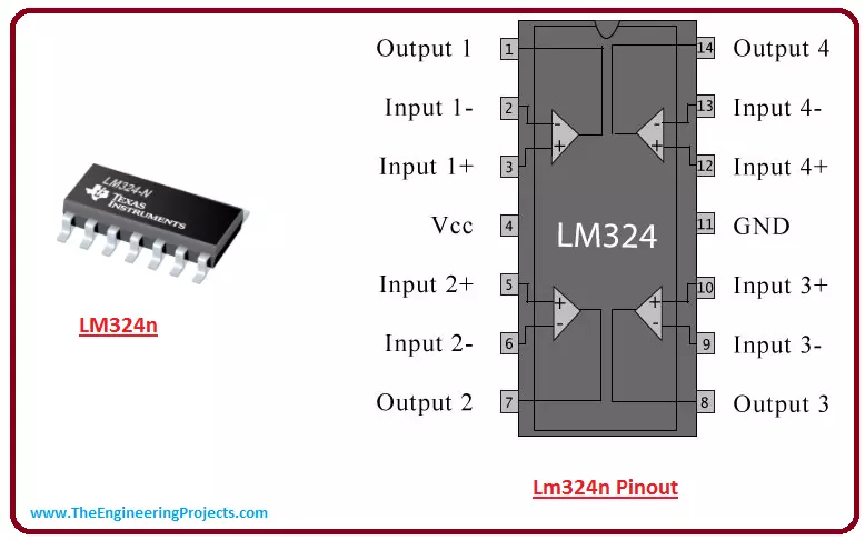
Introduction to Lm324n
Lm324n is a high gain voltage amplifier that comes with differential input and single ended output.
It is designed in such a way, that the voltage difference between input terminals cr ...
Hey Fellas! Hope you are doing great. I am here to give you the daily dose of information relating to engineering and technology. Today, I am going to give you the details on the Introduction to 2sc4617. It is an NPN (negative-positive-negative) transistor which is used for general purpose amplification. This component comes in SC-75/SOT-416 sealed package which is mostly used for low power applications. I am going to explain the brief overview of 2sc4617. Let's get started.
Introduction to 2sc4617
2sc4617 is a three terminal NPN silicon transistor which consists of two N doped layers which cover one P doped layer. It is a bipolar transistor which is usually used for amplification purpose.
Small amount of base current is used to handle the la ...
Hey everyone! Hope you all are doing great. Today, I am going to give you the details on the Introduction to 2n4391. It is a simple N type JFET (Junction field effect transistor) which consists of three terminals called drain, source and gate and are denoted by D, S and G receptively. It is mostly used in analog switches and current limiters. I am going to give you a brief details on this transistor. Let's get started.
Introduction to 2n4391
2n4391 is a field effect transistor that consists of three terminals known as drain, source and gate.
It is called field effect transistors because static field performs as important part in the operation of this transistor.
Unlike normal transistors, it is a voltage controlled device as it doesn't requ ...
Hey Everyone! I hope you all are having fun and looking forward for happy weekend. I am here to give you a daily dose of sound knowledge so you can develop some skills in engineering field. Today, I am going to uncover the details on the Introduction to 2sa1215. It is bipolar silicon PNP (positive-negative-positive) transistor. It is made up of two layers of P doped material and one layer of N doped material. I'll give you the brief overview of this device, what it does and what are its major applications? Let's hop on the board and dive into the details of this PNP transistor.
Introduction to 2sa1215
2sa1215 is a bipolar PNP silicon transistor where one layer of N doped material lies between the two layers of P doped material.
The small cu ...
Hey Everyone! I hope you are doing great. I am back to give you daily dose of information so you can excel in your life. Today, I am going to uncover the details on the Introduction to 5n50. It is an N-Channel MOSFET which is designed to obtain high switching performance and minimum on state resistance in an effective way. It is a unipolar device which comes with three terminals called drain gate and source. I'll try to cover everything in detail related to this N-Channel MOSFET. Let's hop on the board and dive in the details to unlock the features of this transistor.
Introduction to 5n50
5n50 is an N-Channel MOSFET that comes in advanced DMOS, planer stripe technology.
It is designed to achieve high switching performance. As it is an N-Chann ...
Hey Guys! I hope everyone's fine. Today, we are going to have a look at What is MOSFET? We will cover MOSFET Definition, Full Form, Symbol, Working & Applications in detail.
MOSFETs are commonly used in many electronic applications. A number of MOSFETs are added in tiny memory chips or microprocessors that are widely used in cell phones and laptops. It is a voltage-controlled device that is used for amplification and switching purposes. I'll try to touch every area related to MOSFET. Let's get started.
What is MOSFET?
MOSFET is an advanced type of FET, manufactured with controlled oxidation of semiconductor, having 4 Terminals, named:
Drain(D)
Gate(G)
Source(S)
Body(B)
where,
Gate(G) Terminal is practically insul ...
Hey Fellas! I hope you are enjoying your life with love, care and passion. Today I'm going to give you the details on the Introduction to 1n4733a. It is a Zener Diode which works similar to normal diode with only exception, it can also conduct in reverse biased condition. Zener diodes are considered as a basic building components for many electronic circuits. I will try my best to give you the details on almost every feature of this zener diode so you don't need to go anywhere for finding the information regarding this zener diode. Let's get started.
Introduction to 1n4733a
1n4733a is a normal p-n junction diode which allows the current to flow in both directions i.e. forward direction and reverse direction.
In other words, it conducts in bot ...
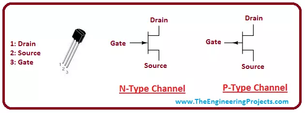
Hello Guys! I hope you are doing great and having fun. I am back to give you a daily dose of knowledge that will enhance your learning skills and put you ahead of others. Today, I am going to give you details on the Introduction to JFET. It is a Junction Field Effect Transistor that consists of three terminals named drain, source and gate. It comes in two configurations called the P-Type channel and the N-Type channel. I'll give you brief details on JFET and try to cover as many aspects as possible. Let's get started:
Introduction to JFET
JFET (Junction Field Effect Transistor) is a uni-polar voltage-controlled device that consists of three terminals called drain, source and gate.
Unlike bipolar junction transistors which are bipolar current-controlled devices in which a small amo ...
Hello Friends! I am back again to fill your appetite with more knowledge and skills. Today, I am going to explain the details on the Introduction to BF259. It is a bipolar NPN (negative-positive-negative) silicon transistors which comes in metal casing. It consists of one P layer that lies between the two layers of N doped semiconductor. I am going to cover all aspects related to this bipolar transistor. Let's get started and have a look, how it works and what are the applications it finds useful.
Introduction to BF259
BF259 is a bipolar silicon transistor which is made up of two N doped layer and one P doped layer.
It is mainly a three terminal device which consists of emitter base and collector.
P terminal of the transistor acts like a ba ...
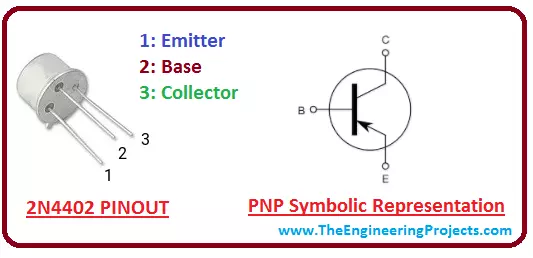
Hey guys! I aspire you a prosperous life filled with joy and happiness. Today, I am going to uncover the details on the Introduction to 2n4402. It is basically a PNP (Positive-Negative-Positive) silicon transistor where N doped layer lies between the two P doped layer. It consists of three terminals i.e. emitter, base, collector. Here N represents the base of the transistor and two P layers represents the emitter and collector respectively. I'm going to cover all aspects related to this transistor. Let's hop on the board and dive in the details of this silicon transistor.
Introduction to 2n4402
2n4402 is a bipolar silicon transistor, where one layer of N doped semiconductor is sand-witched between the two layers of P doped semiconductor.
It w ...