Introduction to 2n2219

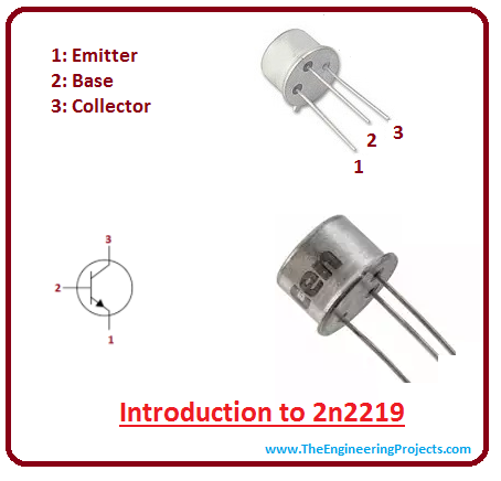
Introduction to 2n2219
- 2n2219 is an NPN bipolar junction transistor which is mainly used for small signal general purpose amplification and switching applications.
- It mainly consists of three terminals called emitter, base, and collector. And the base is positive with respect to the emitter.
- It is termed as bipolar junction transistor because conduction is carried out by both charge carriers i.e. electrons and holes but majority charge carriers are electrons.
- Movement of electrons plays an important role in defining the conducting behavior of this NPN transistor.

- This NPN transistor can be configured with three configurations named as a common collector, common base, and common emitter configuration.
- 2n2219 is a current controlled device where small current at the base side is used to control large current at the emitter and collector side.
- When positive voltage is applied at the base side, electrons start to flow from emitter to collector and base is used to control the number of electrons.
2n2219 Pinout
- Following figure shows the pinout of 2n2219.
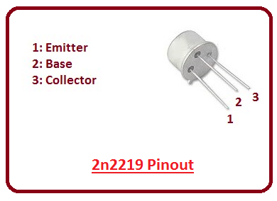
- It mainly consists of three terminals which determine the overall nature of the transistor.
- When a small voltage is applied at the base side, it gets biased and allows the small current at the base side to control the large current at the emitter and collector side.
- Conduction is carried out by the movement of electrons from the emitter to collector and base is used to control the number of electrons.
Circuit Diagram of 2n2219
- The circuit symbol of 2n2219 is shown in the figure below.
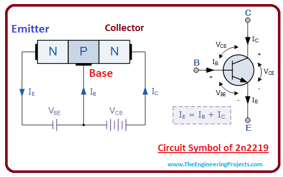
- This NPN silicon transistor exhibits positive base side and negative emitter side.
- Similarly, a voltage at the collector side is more than the voltage at the base side.
- This transistor can be configured into three main configurations called common emitter configuration common base configuration. Common emitter configuration is mainly used for amplification purpose because it features the exact voltage and power gain required for amplification purpose.
- This common emitter configuration allows the input to increase by 20dB which is 100 times more than the input signal.
- Collector and emitter are slightly different in terms of their size and doping concentrations. A collector is lightly doped while the emitter is highly doped.
- This NPN transistor is a bipolar current controlled device which is different than MOSFET that is unipolar voltage controlled device.
- Forward current gain is an important feature that is mainly used for determining the amplification capacity of the transistor. Forward current gain is called beta, usually denoted by ß and is a ratio between collector current to the base current. It is called amplification factor which is a measure of current being amplified. Beta value ranges between 20 to 1000 but its standard value is 200. Beta is a ratio of two current so it has no unit.
- The current gain of this transistor is represented by alpha a which is a ratio between collector current and emitter current. Alpha value ranges between 0.95 to 0.99 and most of the times its value is considered as a unity.
- Both NPN and PNP transistors are different in terms of charge carriers. Electrons are major carriers in NPN transistors while holes are major carriers in PNP transistors.
Absolute Maximum Ratings
- Following figure shows the absolute maximum rating of 2n2219
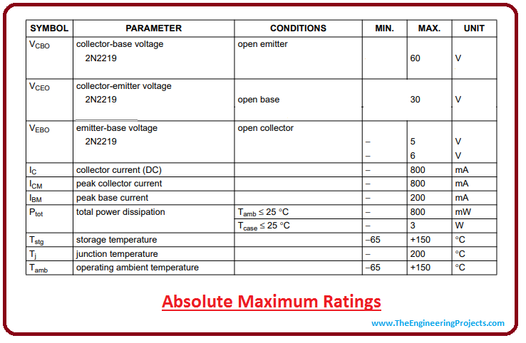
- Collector-Base voltage with open emitter is 60 V. And collector-emitter voltage with an open base is 30 V.
- Maximum Power it can dissipate is 800 mW.
- These are the stress ratings, if these stress ratings are exceeded from absolute maximum rating, they can damage the device.
- Similarly, if stresses are applied for an extended period of time, they can affect the device reliability.
Applications
- It exhibits high current and low voltage which makes it an ideal choice for high-speed switching.
- The ability of a base terminal to control the number of electrons is mainly used for amplification purpose.
×
![]()


