Solar Inverter in Proteus
Hello student! Welcome to The Engineering Projects. We hope you are doing good. We are glad to introduce and use the Solar Panel Library in Proteus. We work day and night to meet the trends in technology. This resulted in the design of new libraries in Proteus Software by TEP and today we'll talk about the project based upon one of our library i.e, Solar Panel.
Solar Panels work very great in this era when all of the scientists are working to have a power source that is cheap, environmentally friendly, and clean. Solar energy fits in all these dimensions. We are designing a solar inverter in our today's experiment. This inverter is the best idea for the engineering project because it has endless scope, it is easy and trouble-free. In this report, you will learn:
- What are solar inverters?
- How do we add the Library for Solar Panel?
- How does the circuit of the Solar Inverter works?
- What is the procedure to design a Solar inverter in Proteus ISIS?
In addition, we'll look at some interesting points in DID YOU KNOW sections.
Solar Inverters
The inverters are the devices that convert the DC power to AC power. These inverters are indispensable because a large number of electronics works on AC and the cons and pros of AC or DC device depends upon the requirement of the device. In this way, we may define the solar inverters as:
"The solar inverters are the devices designed to convert the solar energy stored in the solar panel in the form of Direct current, into the alternating current by the mean of its circuit."
The energy is stored in the form of solar energy that comes directly from the sun. This makes it suitable to use for thousands of devices and users can get the ultimate solution of the power source with minimum or no cost once set up is completed.
DID YOU KNOW?
- The solar panels are also called the photovoltaic module and these are made by the photovoltaic cells that store the energy coming from the sun and convert it into the direct current.
Addition of library for solar panel
As we said earlier, the idea of the Solar Panel lin=brary is new. We design this library to improve the experimentation and many circuits are been design by using solar energy and solar system. When you search for the "Solar Panel", you won't have this. In order to have it in your Pick Library option, just download it from our site. You can add it in really straightforward and easy steps:
- First of all, you need to download the zip file of the Solar Panel Library for Proteus.
- From the downloaded folder, unzip the library files into the Library folder of the Proteus.
You can also read the full description if you have any confusion about the installation.
Components of the Solar Inverter
The Solar Inverter consists of some simple passive components such as resistors, capacitors, diodes etc. along with other components. Out of which, some of them are important to discuss. Just have a look at them:
Solar Panel
Solar Panels are the best source to produce electricity. The Solar cells work when the sunlight strikes the surface of the Solar Panel, the photovoltaic cells capture the sunlight and convert them into another form of energy i.e. electric current. This energy is then stored in the battery or can be used directly to run the devices.
DID YOU KNOW?
- In solar panels, the collection of the photovoltaic Module is called PV Panel.
- On the other hand, the system of PV Panel is usually called an array.
Battery
We all know a battery is used to power up the components in the circuit. yet, in our circuit, the battery will be used to store the energy produced by the solar panel. This process continues until the switch is opened. Once the switch is opened, the battery will be used to run the inverter.
Relay in Solar Inverter
The relay is an engrossing component. It works as the controller of the circuit. The working of the relay seems like the switch but it has a magnetic coil in it that magnetizes and de-magnetizes, according to the requirement of the user. This plays an important part in the charging and discharging of the battery as well as the working of the Solar Panel.
Working of Solar energy Inverter
The Working of the solar inverter starts when the user plays the simulation. In this case, we always assume that the direct sunlight is striking to the solar panel and it is producing energy. We can say, the circuit of the solar inverter consists of 2 mini circuits connected with each other.
- The circuit of the solar panel is the medium of energy.
- The circuit of the battery absorbs the energy coming from the solar panel and releases the energy when the user requires it.
Both of the circuits are joined and disjoined with the help of switches. As far as the switch of the Solar Panel is closed, the circuit does not show any output. When the switch is turned closed(connected) then the energy from the solar panel starts moving towards the relay.
- The Relay is magnetized and it produces the path for current to flow towards the battery and charge it.
- In this mode, if the switch of battery is opened, the LED does not show output, but the battery still charges.
- If the switch of battery is closed, the battery is getting charged and shows the output at a time.
One can stop the charging process by switching the solar panel off. The output of the battery will still be seen because of the charging process until the battery has the energy.
Simulation of the Solar Panel Inverter in Proteus ISIS
To simulate the circuit of the Solar Panel Inverter, go along with these steps:
Material Required
- Solar Panel
- Diode
- Transformer
- LED
- Resistor
- Capacitor
- Switch
- Battery
- Ground
- Connecting Wires
Procedure for the Solar Panel Inverter Simulation
- Fire up your Proteus Software.
- Create a new project.
- Go to the "P" button and choose the 1st eight elements given in the list above.
- Arrange all the components one after the other on the screen.
- At this time, we are going to change the values of some components.
- Change the value of R1=1K, R2= 18, C1=470uF,Battery=9V.
- Connect the components with one another by following the image given next:
- You can see in the image, the red-colored wire shows the voltage and the arrows are indicating the flow of current when both the switches are closed.
- You will notice, as soon as you play the button, the terminal of the Relay changes its position.
- The lights of the LEDs indicate the working of the circuit of the Solar power inverter.
Consequently, we saw about the theory and the practical performance of Solar inverters in Proteus ISIS and we learned how can we add the library of solar panels in the Proteus.
Simplest LM386 Audio Amplifier in Proteus
Hey Learners, welcome to another exciting tutorial about electronics. We are talking about an audio amplifier using LM386. This is a very simple IC that we are going to used for the amplification of the audio signals. We shall go through the core postulation about the topic and then work on the practical implementation of the experiment. Just have a look at the topics of discussion:
- Introduction to LM386 Audio Amplifier.
- Components of LM386 Audio amplifier.
- LM3386 Audio Amplifier Working.
- Simulation of the LM386 Audio Amplifier Circuit in Proteus.
In addition, you will find interesting information in the DID YOU KNOW sections.
Introduction to LM386 Audio Amplifier
Audio signals play important role in many devices. These signals are used to regulate the life of the community in many ways. These signals, when required, are amplified by some means to use them more effectively and efficiently. Many devices can do this task. Yet, at the present time, we are going to discuss LM386 Audio Amplifier. Let's have its definition:
- "The LM386 audio frequency Amplifiers are the types of low power audio amplifiers used commonly in small amplifier systems and can be run on even a 9V battery."
The input signals once pass through the LM386, are amplified and the user senses a loud sound as compare to the input signal. This type of amplification is really important in the circuits where a signal is required to show the completion of the task, requirement of the involvement of the user or an error in the circuits.
Components of the circuit of LM386 Audio Amplifier
In this article, we're using the very simple circuit of LM386 Audio Amplifier to show the easy but understanding hypothesis of the topic. This circuit consists of capacitors, audio signals, LM386 IC, power source and speaker, out of which, we have to discuss the LM386 IC, Audio signals and speaker.
LM386 IC
The LM386 is a versatile chip that can easily be used in many kinds of circuits. The IC runs no low voltage, therefore it is a very common yet power operational amplifier that is used even in DIY guitar pre-amplifiers. If we look at the basic definition of LM386 then we find:
"The LM386 is an 8-pin Dual inline integrated circuit that can work on very low voltage and when connected with some simple components can be used as an operational amplifier in a large number of amplifying circuits."
The power intake and efficiency depends totally upon the models of the LM386. Basically, there are three models of aLM386 IC as mentioned below:
Number of Pin |
Name of pin |
1 |
Gain |
2 |
Negative input |
3 |
Positive Input |
4 |
Ground |
5 |
Gain |
6 |
Bypass |
7 |
Input power |
8 |
Output of IC |
Being an op-amp, the LM386 has a very basic task. The IC gets the power from its input terminals and using its circuitry, it amplifies the power output signal on the rate of tens, hundreds, thousands and so on. The total output purely depends upon the input and the model of LM386.
Speaker
The speakers are the devices that takes the audio signals and convert them into voice. This conversion is done by the special mechanism of speaker. In this experiment, the output will me hear with the help of this speaker.
Variable Resistor
As the name describes, the variable resistor is the special device that is capable of changing the value of resistance according to the requirement of the user. The + and - terminal of variable resistor are used to increase and decrease the resistance respectively. In this way, the input audio signals can be controlled.
Working of LM386 Audio Amplifier
- The working of the LM386 Audio Amplifier starts with the audio signal generation of audio generator.
- These signals passes through the capacitor that regulates these signals and then pass them to the LM386.
- The IC inputs these signals, the pin 6 of the LM386 is connected with the DC Source hence it powers it up. The IC now amplify the audio signals.
- From pin 5 of the IC, the amplified audio signals are generated. Meanwhile, the resistor and capacitor regulates the signal so that the user may sense these signals in the right sequence of waves.
- Finally, the speaker takes these signals as input and convert it in the form of sound so that the user can hear it easily.
Procedure to simulate the LM386 in Proteus ISIS
By availing all the information given above, let's simulate the circuit in Proteus ISIS. Just apply the instructions given below:
Material Required
- LM386 IC
- Resistor
- Capacitor
- POT HG
- Speaker
- Ground Terminal
- Audio device
- Start your Proteus ISIS.
- create a new Project.
- Click on P button.
- Choose 1st five components mentioned in the list given above.
- Arrange all the components on the working area by following the image given next:
- Go to Terminal Mode from the left side of your screen and choose ground. Now, set it just below the circuit.
- Go to Generator mode>choose audio and set it just on left side of arrangement.
- Double click the audio probe>brows>upload this file.
- [audio wav="https://www.theengineeringprojects.com/wp-content/uploads/2021/06/file_example_WAV_1MG.wav"][/audio]
- Change the values of the components as described in the following table :
Component |
Value |
C1 |
1nF |
C2 |
100F |
C3 |
1uF |
C4 |
47nF |
C5 |
47 nF |
C6 |
220uF |
R1 |
10 ohm |
R2 |
10 ohm |
DC Power Supply |
9V |
- Once all the values are changes, just go to virtual Instrument mode and select the oscilloscope above the components.
- At this time, join the components with the help of connecting wires.
- Hit the Play button with your mouse and simulate the circuit.
- Change the values of the voltages of terminals and current through the nobs to get the visible wavelengths.
one can see clearly that the output signal(blue waves) are more amplifier and strong than the input signals (Yellow waves).
Conclusion of experiment
The LM386 is the IC that can be used to amplify the audio signals. The input frequency and thus the volume of the sound amplifies and we can hear the loud sound. One can change the intensity of sound by using the active variable resistor.
Buck Converter using MOSFET Gate Driver in Proteus
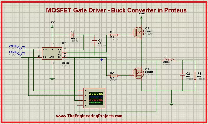
Hey Geeks! Welcome to The Engineering Projects. We hope you are doing great. MOSFET is a predominant component widely used in electronics due to its performance. We are working on the Projects of MOSFET and today's experiment is really interesting. We are working on the MOSFET Gate Driver and we will work on the following concepts:
- Introduction to MOSFET Gate Driver.
- Circuit of MOSFET Gate Driver.
- Working of MOSFET Gate Driver.
- Simulation of MOSFET Gate Driver in Proteus.
- Applications of MOSFET Gate Driver.
You will find important information about the topic in DID YOU KNOW sections.
Introduction to MOSFET Gate Driver
We all know MOSFET is a type of transistor and is used in a wide range of circuits. It has many interesting features and the characteristics of MOSFET are at the fingertips of electrical and electronic engineers. The circuit of the MOSFET Gate Driver may be new for many students so let's have a look at its definition:
"The MOSFET Gate Driver is a type of DC to DC power amplifier that in the form of on-chip as well as discrete module in which we use MOSFET as the gate driver IC, the low power is taken as input from MOSFET and high power is obtained its gate terminal and vice versa according to need."
DID YOU KNOW?
The name of the MOSFET Gate Driver is due to its characteristic to have the high current drive gate input of a Transistor. We use the MOSFET because it is a gate driver IC.
MOSFET is used in this circuit because it is commonly used in switching devices where the frequency ranges from hundred of KHz to thousands of KHz. It is mostly used in appliances where we need DC to DC amplification. It is used in computers to low their temperature during their performance. The MOSFET Gate driver is used to change the value of DC according to the circuit of the appliances.
There are three types of drivers:
- High side drivers.
- Low side Driver.
- Isolated Drivers.
Circuit of MOSFET Gate driver
When we look at the circuit of the MOSFET Gate drive, we found there are some basic as well as some special components in the circuit. In addition to MOSFET, the circuit consists of resistor, capacitor, inductor and IR2101. Let's look at their functions:
MOSFET
- Metal Oxide Semiconductor Field Effect Transistors have a thin layer of silicon oxide between Gate and channel. It four terminals: Gate, Drain, Source.
IR2101
It is IC that works very great with MOSFET. We use it in the MOSFET Gate driver to insert the voltage in the Gate terminal of the MOSFET in the form of pulses. We define the IR2101 as:
"It is seven pins, high power, high voltage, MOSFET and IGBT driver that has independent high and low channel references."
The detail of the pins is given as:
- Vcc: This Pin is for Low side and logic fixed supply voltage.
- Vs: It is for High side floating supply offset voltage.
- Hin: High side gate driver output is taken by this pin.
- HO: We get High side gate drive output through this pin.
- Lin: Low side gate driver output is taken by this pin.
- LO: Low side gate drive output is obtained through it.
- COM: we get Low side return from this pin.
Other components are very common to discuss.
Working of MOSFET Gate Driver
The working of the MOSFET Gate Driver start when the power is generated from power terminals.
- The IR2101 starts with the power terminal, the input pulse generators convert this power into the special length as set by the user.
- These pulses Enter at the gate terminals of MOSFETs.
- Both of these MOSFETs do not turn on at the same time. They work in a loop so that if the high side MOSFET is turned on then the other is off and vice versa.
- The MOSFET M1 on the upper side of the circuit is considered at the High side of the driver and the MOSFET M2, on the lower side of the circuit is at the Low side driver.
- After some time, when the voltage becomes greater than the threshold voltage of MOSFETs, they start working.
- The terminals of MOSFETs are connected with the capacitor.
- The aim of this circuit is to charge the capacitors. Hence when the MOSFET starts working, the charging of the capacitor takes place.
- The pulses reach both the MOSFET at a very specific time due to IR2101.
- Once the capacitor C2 is fully charged, it starts the discharging power and this discharging power from the inductor as well and at last, it goes to the ground terminal.
- In this case, the polarity of the inductor changes and in this way, the energy stored in the capacitor is discharged.
- Hence at the end, when we check on the oscilloscope, we get the changed output pulse from the input.
Simulation of MOSFET Gate Driver in Proteus ISIS
Material Required for MOSFET Gate Driver
- MOSFET
- IR2101
- Resistor
- Capacitor
- Inductor
- Ground Terminal
- Power Terminal
- Pulse Generator
Using all the concepts given above, we'll simulate the circuit in Proteus for a crystal clear concept. Just follow the steps given next:
- Start your Proteus Software.
- Make a new Project.
- Click at "P" button to choose the first five components for the experiment one after the other.
- Arrange all the components in the working area according to the arrangement given next:
- Go to Terminal Mode> Ground and add ground terminal with the required components of the circuit.
- Repeat the above step with the power Terminal.
DID YOU KNOW?
The efficiency of MOSFET Gate driver is more than 90% in many cases.
- Go to Instrument Mode and take the Oscilloscope from there. Now, arrange it just below the circuit.
- Connect all the components with the help of connecting wires by carefully following the image given next:
- Double-tap the components one by one and change the default values according to the table given next:
Components |
Values |
R1 |
10R |
R2 |
10R |
R3 |
60R |
L1 |
500u |
C1 |
4.7u |
C2 |
60u |
Pulse 1 |
Pulse (High) voltage =5v, frequency 1k, Pulse Width 50% |
Pulse 2 |
Pulse (High) voltage =5v, frequency 1k, Pulse Width 50% |
- Tap the play button at the lower-left corner of the screen to simulate the graph.
- Set the values of voltage and current through the nob to see a clear output.
Applications of MOSFET Gate Driver
- MOSFET Gate driver is used in DC to DC converter.
- It is used in the conversion of high voltage to low voltage.
- It is mainly used to reduce heat in many circuits.
- Due to its functions, it is useful in extending battery life.
So, in the present article, we saw what is MOSFET Gate driver. What important components are used in it, how does its circuit works and how can we simulate its circuit in Proteus. Moreover, we also read some of its applications. We hope you learned well from this article.
H-Bridge Circuit with 2N2222 Transistor in Proteus
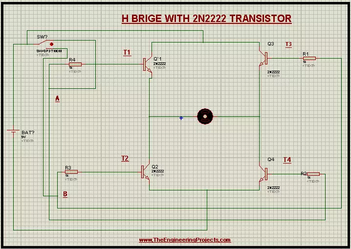
Hey Learners! Welcome to The Engineering Projects. We hope you are doing great. Our team is working on transistors and today, we'll design a circuit for using the 2N2222 Transistor. In this chapter you will learn:
- What is H Bridge with 2N2222 Transistor?
- How do the 2N2222 Transistor works?
- What is the working of H Bridge?
- How can we run the circuit of H Bridge in Proteus using 2N2222 Transistor?
By the same token, you will also learn important information about the topic in DID YOU KNOW Sections.
Introduction to H-Bridge
In electronic circuits, the direction of quantities like the flow of current, EMF, Electric field lines matter a lot. The H Bridge is used to control such motors through its specialized circuitry. The H Bridge is defined as:
"The H Bridge is an elementary circuit that ends the Motors to rotate in forward or backward direction according to the will of the user."
In this way, there is no need for the two motors in many cases. Only one motor can be used to accomplish the task instead of two.
DID YOU KNOW???
The most common, easy and interesting application of the H Bridge is in the robotics. The H Bridge is used to run the motors of the robots that are required to move the robot in the forward and backward direction.
The circuit of the 2N2222 H Bridge allows the current from the Direct Current source to flow from the required direction only and hinders the flow from the other direction.
Why we need the H Bridge
The direction of the moving of a motor paly a vital role in the output of that motor. The reason behind this is, most electric motors operate due to torque produced as the combined effect of magnetic field and electric current through a wire winding. Hence, We always need some means through which we can control the direction of the Motor to get the output that is suitable for our present requirement.
Performance of 2N2222 Transistor in H Bridge
The 2N2222 Transistor works as a backbone in the circuit of the H Bridge. We use four 2N2222 Transistors in the circuit and they work as a couple. The diagonal Transistors work together as a couple and allow the flow of current through them. By the same token, the non-diagonal 2N2222 Transistors work as a couple. Let's have a look at what is 2N2222 Transistor:
"The 2N2222 Transistor is a type of Bipolar Junction Transistors or BJTs that is designed to be used in the low power amplifying or switching applications."
DID YO KNOW???
Motorola made many semiconductor companies and the 2N2222 is part of a huge family of Devices and Transistors that were discussed in IRE Conventions in Motorola company.
Being a BJT Transistor, the 2N2222 allows the flow of current in only one direction. Thus, it is responsible for the rotation of the Motor as per requirement of the user.
The 2N2222 transistor (just as other JTs) has three pins. These pins are called Emitter, Base and Collector. The arrow symbol just at the transistor symbolizes the Emitter.
Being an NPN Transistor, the collector and emitter terminals of 2N2222 Transistor in H Bridge act reverse biased or are said to be left open when the base pin is held to the ground or when there is no current flow from the base.
On the other hand, when the base gets the flow of current from the battery or other components of the circuit in the H Bridge, the circuit is said to be forward-biased. The gain of the 2N2222 Transistor in the H Bridge ranges from 110 to 800. The value of gain is responsible for the determination of the 2N2222 Transistor's amplification capacity in the H Bridge.
Working of H Bridge Circuit
When we look at the circuit of H Bridge we get the following points:
- The Direct Current from the battery originates from the positive terminal of the battery (considering the conventional current) and passes through the switch.
- The switch allows the current to pass through the pair of the 2N2222 Transistor that is to be used.
- The resistors just before the Transistors perform the regulation of the current through the transistors.
- In our case, the H Bridge works according to the table given below:
Switch |
Flow of Current |
Direction of Motor |
Connected to A |
From T4 to Motor then Motor to T1 |
Anti-Clockwise |
Connected to B |
From T2 to Motor then Motor to T3 |
ClockWise |
Let's have a look at the working of the H Bridge in action in Proteus ISIS.
Circuit of H Bridge in Proteus ISIS
We are going to design the circuit of the H Bridge in the Proteus ISIS. But before this, let's have a look at the required devices for the circuit.
Required Devices for H Bridge
- 2N2222 Transistor
- Resistor
- Motor
- Cell
- Switch
- Connecting Wires
Now, just follow these simple steps:
- Start your Proteus Software.
- Click at the "P" button and choose the required devices except for connecting wires one by one.
- Arrange for 2N2222 Transistors, four Resistors, motor, switch and cell on the working area.
- Change the orientation of two of these Transistors before setting on the screen by clicking the arrow sign given just above the "P" button.
- Left Click the motor>Rotate clock-wise to change the direction of the motor according to the image given next:
- Change the value of Cell and Motor to 6v by double taping them one after the other.
- Connect all the components according to the circuit given next:
- Double click at all the resistors and transistors one after the other and label them to identify them as different devices.
- Pop the simulation button.
- Change the orientation of switch and check the output.
Task
Change the value of the transistors around the motor and observe the rotation speed of the motor.
Truss today we saw, what is H Bridge, what is the role of 2N2222 Transistor in the circuit of H Bridge, How does the circuit of H Bridge works and we implemented the H Bridge circuit using 2N2222 Transistor in Proteus ISIS. Stay with us with more tutorials.
12V to 220V Step Up Inverter using transformer in Proteus
Hey learners! Welcome to another exciting electrical experiment in Proteus. At the present day, we'll perform the inversion of voltage. For this purpose, we will use the implementation of Transformer as Step-up Transformer. Prior to start, let's have the basic information about the 12V to 220V Step up inverter using Transformer in Proteus. In this tutorial, we'll learn:
- What is a 12V to 220V inverter?
- What is the function of the transformer in the 12V to 220V inverter?
- How can we implement the Step up inverter using a Transformer in Proteus?
- What are some applications of the 12V to 220V inverter?
Moreover, there will be some useful pieces of information in DID YOU KNOW sections.;
12V to 220V inverter
In electronic appliances, the circuitry is designed so, that the appliance can work in a specific range of Voltage, Frequency and power etc. If these quantities are not supplied using these parameters, then the Appliance does not work ideally. For example, if the given voltage to a bulb is less than its voltage range it may be lightened dim. or if the voltage is given more than the range of the bulb, the circuitry of the bulb may be damaged or even it may burst.
In such a case, the invertors are used that inverts the voltage (or other electrical quantities according to type) into the suitable range is used. Therefore, the 12V to 220V inverter can be defined as:
"An invertor is the electrical circuit that converts the 12V Direct current into 220V Alternating current and alters supplied voltage range into required range."
By using the 12V to 220V inverter the electrical or electronic circuits, we can use the electrical circuits that work on the 220V even when the supply from the source is 12V.
DID YOU KNOW??????????????
"The Inverters play a life saving role in the appliances that have a sensitive circuit to voltage and current. Even the High voltage more than the range of the device can burn the circuit so badly that it may require to change the whole circuitry or the motherboard of the device."
Working of 12V to 220V invertor
in the process of 12V to 220V inversion, three major process takes place:
- Supply
- Conversion
- Transformation
We use simple circuitry to perform each task. Based upon the functionality, we use three devices in the circuit of 12V to 220V inverter. These are:
- Battery
- Transistor
- Transformer
Role of Battery in 12V to 220V Transformer
It is obvious that every circuit requires some sort of energy to perform the required function. In 12V to 220V Inverter, we use a 12V battery that will be supplied to whole components. The 12V battery performs the "Supply" process in the 12V to 220V Inverter.
Role of Transistor in 12V to 220V Inverter
The process of conversion of direct current into alternating current requires a mechanism that allows just the positive side of the sinusoidal wave of the Alternating current to pass through it and hence one can get only one side of the output wave of current.
In the case of low and medium applications, power Transistors are used. The reason behind this logic is, the Transistors:
- are Less in cost.
- have low output Impedance.
- Allow most of the power to pass through it.
We know that the Transistor work as a switch. the two type regions of the characteristic graph of the Transistor are used in this experiment.
Saturation region: In this region the transistor is biased. The collector-Emitter and the Collector-base junctions are forward biased. The collector has the minimum voltage and the collector current is maximum.
Cut-off Region: In this region, the Transistor does not allow the current to pass through it.
Role of Transformer in 12V to 220V Inverter
The Transformer is the mechanical device used o transform the voltages from its input to its output. It has two sides that have coils around them. In our experiment, we use the Step-up Transformer that is introduced as:
"The type of Transformer that is used to convert the low voltage and high current supplied to its input to the high voltage and low current at its output is called the step up Transformer."
Hence the voltage from the Transistor that is rectified and has the direction only on one side is fed at its input. The Transformer transforms the low voltage into the high voltage. In this way, we get a high voltage. The ability of the transform to amplify the voltage depends upon the number of turns of the coil on its terminals.
DID YOU KNOW???
"If you get a transformer that have the same mechanical structure but it has the numbers of turns in primary coil grater than the secondary coil then it is called the step down Transformer. "
Implementation of 12V to 220V inverter using Transformer
At the present moment, we'll use all our concepts given above to design the circuit for the 12V to 220V Inverter. Just follow the simple steps given next.
- Power up your Proteus circuit.
- Choose the material given below.
Material Required
- 3WATT68R (This resistor works at the 68R resistance automatically.)
- Battery
- Lamp
- MJ-2925
- Trans-2P3S (Step-up Transformer)
- Click at the components one after the other and arrange the components one after the other at the working area.
- Left-click at the Battery and choose "Rotate 180 degree".
- The screen should look like this:
- Change the values of some of the components by following the table given next:
Devices |
Values |
Battery |
12V |
Bulb |
240V |
Bulb Resistance |
100k |
Transformer Primary Inductance |
100H |
Transformer Total Secondary Inductance |
1.1H |
- Connect the elements with the help of the diagram given below:
- Simulate the circuit by clicking at "Play" button given on the lower-left corner of the screen.
You will observe that the bulb is light although it is set as a 220V device and the supplied voltage is just 12V.
Applications of 12V to 220V Inverter using Transformer
- To charge the small batteries of vehicles such as cars.
- Low power Alternating Current Motors.
- Solar Power system.
- Uninterrupted Power Supplies (UPS).
- Reaction power controllers.
- Adapted power Filters.
Adjustable speed Alternating Current Motor Drivers.
Consequently, we saw about an electrical circuit today that converts the 12V from its input to 220V at its output using the Transformer. This experiment has many interesting applications. Stay with us for more experiments.
Digital Counter using 4026 IC in Proteus ISIS.
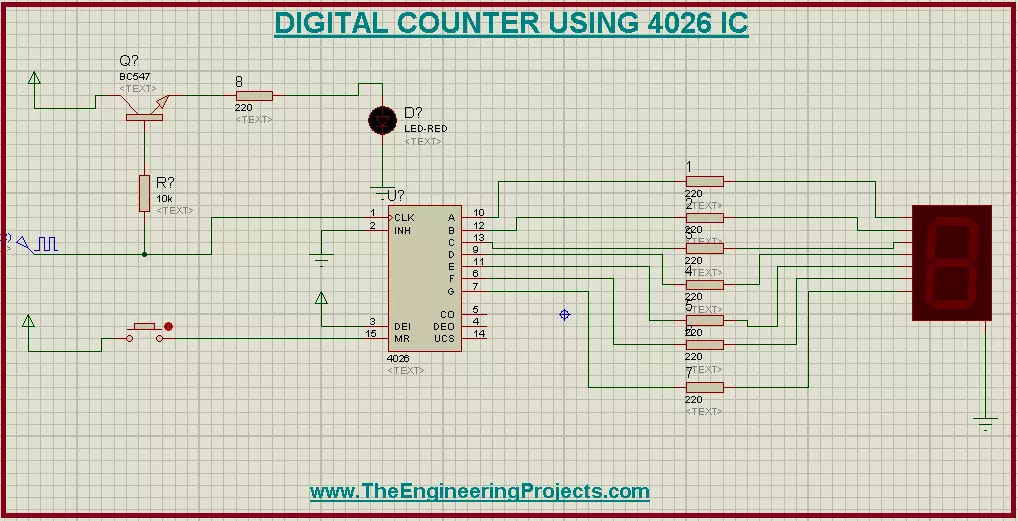
Hello Mentees! Welcome to the board. We hope you are doing great. We are working on another interesting yet easy Project in the Proteus ISIS and that is Digital Counter using 4026 IC in the Proteus. Counters are used in thousands of electronic experiments as well as in our daily life. Who is not5 familiar with Digital Watches and calculators. At the same token, the counters are used in the digital display microwave ovens and many household appliances as well.
In this session you will find the answers to the following questions:
- What is 4026 IC?
- What are Digital counters using 4026 IC?
- How does Digital Counter using 4026 IC works?
- How does we design the circuit of the Digital Counter circuit using 4026 IC in Proteus ISIS?
- How can you convert this Circuit from 1 digit counter to many Digit Counter using 4026 IC?
In addition, you will also have some interesting chunks of information about the topic in
DID YOU KNOW sections.
What is 4026 IC in Digital Counters
Integrated Circuits play a vital role in the field of circuits and electronics. These are the combination of different fundamental devices in very specific yet functional ways. The 4026 belongs to the family of the Integrated Circuits in the series of 4000. The 4026 IC is introduced as:
"The 4026 is CMOS seven Segment counter integrated Circuit that is the designed in decade Based and counts in the decimal digits and consist of total 16 pins."
The output of the 4026 digital counter is usually fed into a 7 segment display Light Emitting Diode that shows the counter output of the 4026 IC Counter.
Being an IC, the pins of the 4026 Digital counter IC are very specific. By looking at the block diagram of 4026 IC Counter, we can generate a table that shows us the proper configuration of the 4026 IC.
Pin Number |
Pin Name |
Description of the Pin |
1 |
Clock (CLK) |
With each positive clock Pulse, it increments the counter. |
2 |
CI (Clock Inhibit) |
It is the Active high. When high, the counter freezes. When low, the clock pulse increments 7 segments. |
3 |
DE (Display Enable) |
Chip will ON when this is high and vise versa. |
4 |
DEO (Display Enable Out) |
Chaining 4026s. |
5 |
CO (Carry Out) |
It completes a single cycle after every 10 clock input cycles. It is used to change the clock manner of 1 counter into a multi counter. |
6 |
F |
This Pin is connected to ‘f’ of the 7 segment. |
7 |
G |
This pin is connected to ‘g’ of the 7 segment. |
8 |
VSS |
It is the Ground PIN |
9 |
D |
It is Connected to ‘d’ of the 7 segment. |
10 |
A |
It connects with the ‘a’ Pin of the 7 segment. |
11 |
E |
It Connects the ‘e’ of the 7 segment with it. |
12 |
B |
It Connects to the ‘b’ of the 7 segment. |
13 |
C |
It is Connected to ‘c’ of the 7 segment. |
14 |
UCS ( Un-gated C-Segment) |
It is an output for the seven-segment's C input that is not affected by the input of DE . When the count is 2, it is high. |
15 |
RST (Reset) |
Reset the counter to 0 when HIGH. Hence it is Active High. |
16 |
VDD |
Power supply PIN |
In out experiment, we'll set all these pins according to our requirements to get the desired output. but some of the points here are pending to discuss. You may noticed the functioning of 6, 7, 9 to 13 pins of 4026 IC Counter. Let's have a look what does we mean by the description.
Seven Segment Display with 4026 IC Counter
This is the electronic device that is used to show the output of the counters such as 4026 IC. We define the Seven Segment Display as:
"The Seven Segment Display is a collection of 8 Light Emitting Diodes in a rectangular fashion that is an output device used to display the outcomes of different counters."
For the convenience of connections, each LED of the Seven Segment Display is named i alphabetically and hence each pin of Seven Segment Display is connected with pins of 4026 IC Counter.
Working of 4026 IC Digital Counter
- The Simulation of the circuit starts with the pulse generation at the Clock Pulse. These Pulses enters the BC547 MOSFET that regulates the pulses.
- The LED Connected to the BC547 MOSFET blink and we get the idea about the speed of the Pulse Generation.
- The Pulse enters the 4026 IC Counter and the counter Passes these pulses to the seven segment Display device.
- Each pulse from the 4026 IC power ups the respected LED of the seven segment display in a specific manner that we always get the digit as a result.
- The power is then Grounded connected to the seven segment display terminal.
- The output can be reset to the initial state with the button. This button is connected to the reset terminal of 4026 IC.
DID YOU KNOW ???
"You may skip the part of MOSFET and LED in the circuit but in some cases, when the error of the pulse occure, it may be difficult to examine whether the Pulses speed is low or there is another issue with the circuit."
Circuit Design of Digital Counter using 4026 IC in Proteus
- Fire up your Proteus Software.
- Choose the first five devices given next from the Pick Library.
Material Required:
- Seven Segment Cathod LED
- Resistors
- 4026 IC Counter
- MOSFET BC547
- Button
- Clock Pulse
- Led
- Ground Terminal
- Power Terminal
- Arrange the material taken from the Pick Library at the working screen with the help of following image:
- Go to generation mode and choose "Clock Pulse" then arrange it just after the left most resistor at the screen.
- Go to Terminal Mode and get "Power" terminal. You will use three Power Terminals.
- Attach power Terminal with pin 3 of 4026 IC Counter, with the MOSFET.
- Get a ground terminal from terminal mode and attach it with the lower pin of seven segment display.
Repeat the above step for the pin 2 of the 4026 IC Counter.Tip of circuit
"Why don't you try different colors of the seven Segment Display from the Proteus Pick Library of your choice?
You have to change the names of the components by double clicking it and changing the label because Proteus does not recognize the components with the same names and through an error."
- Change the values of the Components by double tapping them with the cursor.
Component |
Value |
Resistor 1 to 8 |
220 Ohms |
Resistor 9 |
10k |
Frequency of Clock Pulse |
1 Hz |
- Connect all the components with the help of connecting wires. Be careful with connection and follow the image below:
- Hit the play button to simulate the circuit.
Two Digit Counter using 4026 IC
If you want to make a two Digit counter, simply select the 4026 IC and Seven Segment Display>left click>click "block copy".
- Paste this block at the screen.
- Manage both the Seven Segment Displays side by side.
- Change the names of the Resistors and 4026 IC to resist the duplication.
- Connect the Pin 5 of 1st 4026 IC with the Pin 1 of the 2nd 4026 IC.
- Connect Pin 15 of 2nd 4026 IC with the button given above.
- Pop the Play button again and observe the result.
Result
- When the Frequency of the Clock Pulse is 1. The Digital counter 4026 IC shows us the value from zero to one in normal speed.
- Clicking the button resets the 4026 IC Digital Counter to the initial value, i.e, zero and starts the cycle.
- Changing the value of clock pulse to 10 will increase the digits changing the speed of the seven segment Display output.
- In two digits 4024 IC Counter, we can count the values till 99.
- One can make the 3, 4 and so on digit counter using the same method.
Consequently, we learned an Interesting Circuit today, we saw what are the 4026 IC counter and with the combination of Seven Segment display and Transistor , how can we design a Digital counter circuit in the Proteus. Stay connected for other interesting circuits on The Engineering Projects.
Automatic Light Detector using LDR in Proteus
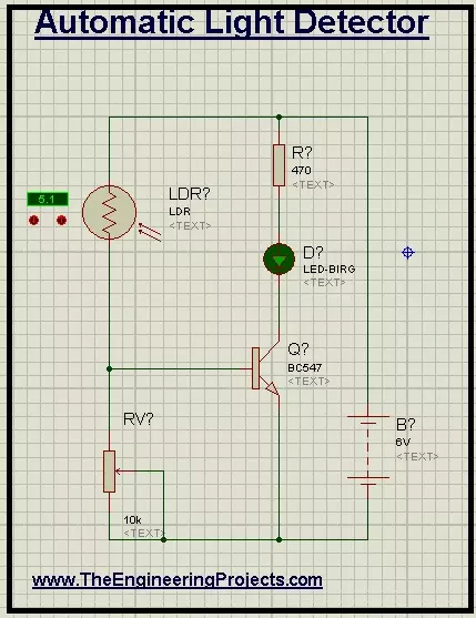
Hello Learners! We hope you are fine. Welcome to The Engineering Projects. The Automatic Light Detector is the device that automatically senses the light incident on it. Let's have a glance about the main points of discussion:
- What is Automatic Light Detector?
- What are different components and their functions in the Automatic Light Detector?
- How does the circuit of Automatic Light Detector works?
- How can we implement the circuit of Automatic Light Detector in Proteus ISIS?
Moreover, you'll have some chunks of interesting information in
DID YOU KNOW sections.
Automatic Light Detector
Automatic Light detectors or automatic Light sensors are interesting devices. They have special mechanism in their circuit that senses the density of the light and after that, the mechanism automatically changes the condition of the Light detector according to the need. Thus an Automatic Light Detector is defines as:
"An Automatic Light Detector are the photoelectrical devices that works with the principle of flow of current and turn the circuit components on/off automatically when the light incidents on its circuit."
The Automatic Light Sensor is an elementary electrical component Which is usually used to handle the electrical Appliances such as coolers, fans, lights etc. without any manual efforts. In this way the manually switching of the electrical components can be controlled more easily. Their working depends upon the intensity of light around them.
DID YOU KNOW????????????
A very simple and usual application of the Automatic Light Detector is the Automatic Street Lights system. Have you ever noticed that there are hundreds of street lights around you when you go for a ride. If someone had a duty to turn them on and off manually, even they have a combine circuit. But it would be a time taking job. Moreover, there will be more chance of energy wastage. But all the street light have the Automatic Light Detector system so that they turn on and off automatically.
Components of Automatic Light Detector
Prior to start the construction of the circuit, Let's have some brief about the components of the circuit for Automatic Light Detector. The circuit that we'll use depends upon the following components:
- LDR
- n-p-n Transistor
- Simple
- Variable resistor
- Battery
- LED
LDR in Automatic Light Detector
LDR or Light Dependent Resistor is the heart of Automatic Light Detector. These are the electronic components, made up of high resistance semi-conductor material, that detect the light and alter the operation of the whole circuit according to the type of the circuit. The LDR is passive and it does not produces any electrical energy. LDR are used in many cases because of their rugged nature. They are not sensitive to dirt and rough environment and therefore have a long life and can be used in outdoor lights.
Other different types of Light Sensors are:
- Photodiode
- Photo-voltaic cells
- Photo-multiplier tubes
- Charged Couple Devices.
n-p-n Transistor BC647 in automatic Light Detector
The full form of n-p-n Transistor is the negative positive negative Transistor. In this type of It is designed to pass electrons from emitter to collector. so the emitter "Emits" the electrons to the base. Obviously, in case of conventional current the current flows from the collector to the emitter. In this Circuit the base of the n-p-n Transistor is connected with the one end of variable resistor and the LRD, emitter is connected with the battery and the variable resistor and the collector is joined with the LED directly.
Resistors in Automatic Light Detector
Resistors are the passive devices consist of two terminals and the body. These are the electric components that are widely use to resist the sudden flow of electricity through a circuit. In many case, they are life saving for the components of the circuits. Other uses of resistors includes:
- Bias active elements
- Terminate Transmission lines
- Adjust signal level to device voltage.
The Automatic Light Detector uses two types of resistors:
- Simple Resistor
- Variable Resistor
The key difference between them in the circuit of Automatic Light Detector is, the resistance (Resisting ability) of variable resistor may be change according to the need of time.
Battery in ALD
A battery is the Lead-acid type cell that consists of the collection of four 1.5V D battery cells. It gives the energy to the components of the circuit for their functioning. The Battery will give the power to the circuit so that the flow of the current will illuminate the light or pass through the LDR.
LED ALD
The full form of LED is the Light Emitting Diode. It is a simple device used in our daily life as well that illuminates when the energy in the form of current or voltage is applied to it. In our circuit, the main function is the turning the on/off of this LED.
Working of the Automatic Light Detector Circuit
When we look at the circuit of Automatic Light Detector, we found that the whole working start from a 6v DC Battery. This battery give the energy to the circuits.
At the day-time the LDR has a low resistance of about 100 ohms. In this case, the resistance of the LDR is less than the other devices of the circuits and we all know that:
The current passes through the path that shows the less resistive path.
The power from the battery passes through it and then from the variable resistor easily.
At the Night-time when the light, incidents on the LRD is less , the resistance of LDR increases to a high level of approximately 20 mega ohm. Due to this high resistance, the LDR act as an open circuit and does not allow the flow of current through it. For this condition, the current will flow from other components of the circuit and hence the current enters o the base of the n-p-n Transistor BC545. This allows the current to pass from the LED and hence it illuminates.
Automatic Light Detector in Proteus
Before any practical implementation, one should always check it in the simulation for practice. Luckily, for our experiment, the Proteus contain all the components through which we can check the functionality of Automatic Light Detector.
Fire up you Proteus software and Choose the components one after the other. Once selected, design a circuit of Automatic Light Detector by following these simple steps.
- Get the Components from the Pick Library and arrange them according to the Circuit diagram.
- Double tap the each components except n-p-n transistor and change their values according to the table given below:
Component |
Value |
Resistor |
470 ohms |
Variable Resistor |
10k ohms (At the start) |
Battery |
6 volts |
- Connect all the components by the mean of connecting wires.
- Simulate the circuit.
- Check the working of circuit by changing the values of the Light Detector Resistor.
- Above 5.1 value of the LDR, the LED illuminates because of high resistance, the current flows through the LED.
- Below 5.1, the LED remains off.
Applications of Automatic Light Detector
Some of the practical applications of Automatic Light Detector are given below;
- Automatic Light system.
- Light measuring instruments.
- Relative distance devices.
- Alarm system.
- Security Systems.
Truss today we learned about the Automatic Light Detector/sensor. we saw what components are present in its circuit, how the system works and how can we implement it in the Proteus software. We hope you had an interesting piece of study through our article.
Boost Converter using MOSFET IRFZ44N in Proteus
Hello Learner! Welcome to another exciting experiment at The Engineering Projects. We hope you are having a great day. In this lecture, we'll seek information about the Boost Converter Circuit from scratch to result in quick and easy steps. So, if you don't know about the experiment then don't worry because every Expert was once a Beginner. We'll talk about the following topics:
- What is IRFZ44N MOSFET Boost Converter?
- What is the brief introduction of components of circuit?
- How can we implement the IRFZ44N MOSFET to design circuit of Boost Converter?
You will know some useful information about the topic in the
DID YOU KNOW sections.
IRFZ44N MOSFET Boost Converter
During the experimentation of electronic circuits, we often face the situation when we have to amplify the voltage signals or voltage power. For example, when we need the 12V in the experiment but we have just 9V battery or any such case. There are many ways to tackle such condition but it requires a lot of energy and steps. But when we search our solution in the world of Switched Mode DC-DC Converters, we find a very easy and simple solution of our problem in the form of IRFZ44N MOSFET Boost Converter.
NOTE:
One can make the BOOST Converter using one of many MOSFETs but we have focus on IRFZ44N due to its best result.
Prior to start the experiment, it is compulsory to have some basic information about the circuit. We define the IRFZ44N MOSFET Boost Converter as:
The Boost Converter is the Electronic device that uses a MOSFET (IRFZ44N MOSFET in our case) to convert it's Low input DC Power into High output DC power.
The IRFZ44N MOSFET Boost Converter is a switched-mode power supply and this is consist of at least two semi-conductor device and minimum one energy storage element.
DID YOU KNOW????????????????
We call IRFZ44N MOSFET Boost Converter as Switched Mode Devices because basically, they are the semi-conductor Switches that turns their condition On and Off very rapidly.
Components of IRFZ44N MOSFET Boost Converter
Throughout the experiment, we'll use the components that will convert the low level Voltages into High Level Voltages. A brief introduction of the components is given next:
IRFZ44N MOSFET
The IRFZ44N Metal Oxide Semi-Conductor Field Effect Transistor is used as a switch in the IRFZ44N MOSFET Boost Converter. The main reason behind this is one can change its conductivity by changing its Gate Voltage and hence we can use it as a switch. This is one of the key procedure to amplify the voltages in the IRFZ44N MOSFET Boost Converter.
Inductor
We all know an inductor is a passive two- terminal magnetic storage device that stores the energy due to its coiled shape. Due to its storage capability, it resists the sudden change of current in the IRFZ44N MOSFET Boost Converter. In this way, it work as a stabilizer in the circuit and play an important role.
Diode
A diode is a reverse biased component of the IRFZ44N MOSFET Boost Converter. It is designed in such a way that it allow the flow of current only in one direction. Hence, in the IRFZ44N MOSFET Boost Converter the Diode allow the flow of current from inductor to the capacitor in only in the condition when it is forward biased.
Capacitor
A capacitor is a device that stores the energy in the form of charges. In IRFZ44N MOSFET Boost Converter when the Switch is turned off, the diode does not allow the flow of current through the capacitor. This is the condition when the stores energy in the form of charges from capacitor is used and the capacitor then works as the source of energy in IRFZ44N MOSFET Boost Converter.
Output graph
Before this we saw the components that we'll use in the formation of circuit, but we require other components as well to examine the result and working. We examine the result through an output device that shows us the result in the form of graph. For our experiment, we'll use analogue analysis graph for the output.
IRFZ44N MOSFET Boost Converter simulation in Proteus ISIS
Fasten your seatbelts because we are going to perform the experiment in Proteus using all the concepts given above.
Material Required
- Capacitor
- Inductor
- DC Power source (Vsource)
- Diode
- Resistor
- IRFZ44N MOSFET
- Voltage Probe
- Ground Terminal
Procedure:
- Press the “P” button and select the first six components one after the other.
- Arrange the selected Material one after the other according to the given diagram.
- Go to Terminal Mode>Ground and set the Ground Terminal with the Vsource.
- Connect all the components through wires.
- Go to Generation Mode>pulse and attach the pulse generator with the Drain of the IRFZ44NS MOSFET.
- Set the values of the Pulse Generator as shown in figure:
- Double click the components one after the other and set the values of components according to the table given below:
Component |
Value |
Capacitor ( both) |
100uF |
Inductor |
39uH |
Voltage |
4V |
Resistance |
15 ohm |
- The Circuit should look like the image given below:
- Connect a Voltage Probe just above the Resistor R.
- Go to Graph mode>Analogue and set a Analogue graph window just below the Circuit.
- Drag the Voltage Probe and drop it just at the Analogue analysis Graph.
- Left Click the Graph>edit Properties and set the value of stop time as 10m.
- Left Click the Graph>add trace and add the value of the probe.
- Again left click the Graph and simulate it. you will find result.
So, today we saw what is IRFZ44N MOSFET Boost Converter, how its components work and how can we implement it in the Proteus ISIS. Stay connected with us for more easy, useful and interesting electronic tutorials about Proteus. Stay updated and blessed.
IRFZ44N MOSFET Characteristic Curves in Proteus ISIS
Hello Learners, Welcome to another useful tutorial at
The Engineering Projects. In the world of electronics and circuits, many useful devices are designed that can minimize the requirement of large and complex circuits. At the Present time, we are working at such a device works very near to the base of many circuits i.e, IRFZ44N MOSFET. We'll approach to the answers of following Questions:
- What is IRFZ44N MOSFET?
- How is the Structure of IRFZ44N MOSFET?
- What is the working mechanism for the IRFZ44N MOSFET?
- How can we find the characteristics of IRFZ44N MOSFET in Proteus ISIS?
You will have some important chunks of information about the topic in
DID YOU KNOW sections.
What is IRFZ44N MOSFET
As you can see, MOSFET is a acronym of
Metal
Oxide
Silicon
Field
Effect
Transistor. We introduce the IRFZ44N MOSFET as:
IRFZ44N is an important type of N-type MOSFET that consist of three pins, have a hgh Drain current and a low Rds Values.
It is the type of IGFET( Isolated Gate Field Effect Transistors). A large amount of MOSFETs are used as switch every year. When we compare it with BJT , we find that it requires almost not current to control the load current unlike BJT. If you want in-depth study on this mosfet then you should have a look at
IRFZ44N Datasheet.
DID YOU KNOW ???
MOSFET is a semi-conductor device that is Fabricated by the Controlled oxidation of Semi-conductors (Silicon in most case). It can work in both modes of operations i.e, Depletion and enchantment.
Structure of IRFZ44N MOSFET
When we observe the
IRFZ44N MOSFET we find that it consist of mainly three pins as described below:
Pin Number |
Pin Name |
Role |
1 |
Gate |
Controls biasing |
2 |
Drain |
Current input |
3 |
Source |
Current Output |
Vgs: The IRFZ44N MOSFET is a voltage controlled device that means it can be turned on and off when we apply a required threshold Voltage. This voltage is termed as Vgs.
Vds: It is the absolute Maximum Voltage of IRFZ44N MOSFET between Drain and Source. This is salient characteristic of IRFZ44N MOSFET because during the operation of IRFZ44N MOSFET Drain-source voltage should kept less than maximum rated value. Here
D Stands for Drain and
S stands for Source.
Ids: It is the amount of current that passes from Vds to the IRFZ44N MOSFET. The direction of this current is important during the Operations of IRFZ44N MOSFET.
DID YOU KNOW ???
The MOSFET is a better version of Junction Field Effect Transistor. Due to the limitation of JFET for the conduction in one side only ( some time it is the advantage), the Designers made a new type of Transistor that can change the conductivity when the amount of applied voltage is change and named them as MOSFET.
Characteristic Curve of IRFZ44N MOSFET
The quality and the suitability of any transistor is checked through its characteristic curve. The characteristic curve of IRFZ44N MOSFET have two phases.
- Depletion Mode
- Enhancement Mode
Depletion Mode
In this mode the Transistor is closed during the zero bias voltage at gate terminal. Hence the IRFZ44N MOSFET is said to be switched ON. The channel width increases when the Gate Voltage is increased to the positive side. in return, the current Ids increases.
During the situation when Gate voltage's value is decreased, the Width of the channel decreases and Ids follows the same rule.
DID YOU KNOW ???
The IRFZ44N MOSFET is also known as the Power MOSFET. It is 22oAB through hole package that has three pins. The top metal tab is also called the drain because both of them are same.
Enhancement Mode
This mode is usually considered as normally open switch as the transistor does not conduct the current when the Gate Voltage is zero. If we apply a positive voltage to the gate then a Drain current follows through the Gate.
The Enhancement mode of IRFZ44N MOSFET enhances the channel because when the Drain current's value is increased the channel width increase and the decrement of the width is for vise versa.
IRFZ44N MOSFET Characteristic Curve in Proteus ISIS
To understand the whole discussion mentioned above, Let's make a characteristic Curve of IRFZ44N MOSFET in Proteus ISIS. To do this, just follow the simple steps given next:
- Power up your Proteus software.
- Go to Pick Library by pressing the "P" button given at the left side of the screen.
- Choose IRFZ44N MOSFET.
- Arrange the Transistor at the working area.
- Go to Terminal Mode from the left most side bar of the screen.
- Choose Ground Terminal and set it just below the IRFZ44N MOSFET.
- Go to Generation mode and select DC.
- Set one DC probe at the left of the irfz44n MOSFET and take another and set it at the upper side of irfz44n MOSFET.
- Connect at the components set until now with the Help of Connecting wires.
- Select the current probe and set it just after the Vds. Make sure its direction is toward the irfz44n MOSFET.
- Go to Graph Mode>Transfer and set a Transfer Graph just after the Circuit.
- Right Click the Graph>Edit Properties>Set the Vds as Source 1>Set Vgs as Source 2>click Ok.
- Right Click the Graph>Add Trace>Set Ids as the Probe>Click ok.
- Right Click the Graph>Simulate.
- You will Get the required output:
Hence, in this article, we learned about the IRFZ44N MOSFET, we saw the introduction of IRFZ44N MOSFET, Learned about the structure of IRFZ44N MOSFET, saw some important concepts about the IRFZ44N MOSFET and performed a Practical Implementation of IRFZ44N MOSFET for the Characteristic Curves in Proteus ISIS.
Junction Field Effect Transistor (JFET) Simulation in Proteus ISIS
Hello Learners, hope you are doing well. I am here with a new tutorial. We'll discuss about
Junction Field Effect transistors. In this tutorial, we will learn the basic Introduction to JFET nad will also have a look at its practical Implementation and simulation in Proteus.
Basically, Junction Field Effect is a type of transistor, similar to Bipolar Junction Transistors but they have different characteristics due to some reasons as discussed below:
Introduction to JFET
We Define the JFET as:
"Junction Field Effect transistors or simply JFET is the semiconductor ,Voltage Control, three terminal device that is present in both configurations either N channel or P channel."
JFET are named so because the the operation of JFET relies on the Field of the input gate voltage thus they are voltage operated devices.
The Input of JFET is called
Gate whereas, the output is said to be
Drain.
Explanation about JFET
Junction Field Effect Transistors are important Devices in the world of electronics. They look similar to the transistors but are different in their Production.
Terminals of JFET:
JFET's have two Ohmic connections at either side of the channels. These channels are called
Source and
Drain. the Connection of Drain and source is said to be
Gate. This is the point where PN Junction is formed.
Source and Drain Collectively makes resistive path through which the current
Id passes due to the Voltage
Vds. The channel is semiconductor due to which current is passed equally well at both sides. But, because of the resistivity of the channel, the voltage becomes less Positive when we move from Drain to Source.
Subsequently, the PN junction contains the high reverse bias at Drain as compared to the Source. Thus, the a
Depletion Region is formed due to biasing whose width increase with the increase in the Biasing and vise Versa.
Configuration of JFET:
We know that Transistors are made by two type of materials i.e, N type and P type. The Terminals are connected by a current path between Drain and Source. these two terminals work as Collector and Emitter, respectively. Hence we observe two Configurations of JFETs:
- N-Type.
- P-Type.
Within the P-Type Configuration, we observe the doping of acceptors. hence holes are abundant in this region. by the same token, N- type configuration contain the doping of the electrons hence we get the faster conduction in N-Type region.
We'll use N type JFET for the experiment.
Types of JFET:
Base upon their Production, we classify the JFET in two types:
- Standard JFET
- Insulated Gate JFET
The 2nd type i.e, IGJFET is most Commonly called Metal Oxide Junction Field Effect Transistor or simply MOSFET.
Conduction of JFET:
JFET are unipolar Devices and their efficiency mainly depends upon the Conduction of holes and electrons in P-Channel and N-channel, respectively.
Implementation of JFET in Proteus ISIS
The Junction field effect transistors has very specific characteristics that can easily observed on the graph at a glance. Hence, let's start the simulation for best understanding.
Material Required:
- Junction Field Effect Transistor (2N3819)
- DC Power Supply
- Ground Terminal
- Current Probe
- DC Transfer Curve Analysis
Procedure for the characteristics of JFET:
- Fire up your Proteus Software.
- Pick Up the JFET from the Pick Library through the "P" button.
- Set the JFET on the working area.
- Foster the "DC" from the power Generation mood of the Proteus.
- Fix 1 DC power supply at the Gate Terminal and the other on the Drain Terminal.
- Pick the Ground terminal from "Terminal mode" and fix it with the Source.
- At this stage, the circuit should look like the picture given below:
- Place the Current probe taken from the side of the Proteus at the Drain.
One point must be clear here, the direction of the probe should be towards the drain showing that the current passes from the Current source towards the Drain terminal of JFET.
- Name the Gate source as "Vgs".
- Name the Drain power supply as "Vds".
- Mark the Current Probe as "Ids".
- Choose "Transfer" from the Graph mode at the left most bar of the Proteus.
- Click on the Working area and make a window of the "DC Transfer Curve Analysis".
- To get the output, we will drag the Id at the graph area.
- At the instance, we have to set the Graph according to our need. Truss, Double click the graph to edit the Properties.
- Set the Values according to diagram:
Now, when we simulate the graph by left click>simulate the graph, we find a simulation log.
- Simulate the graph through the Play button.
- Maximize the screen through left click at Graph>maximize and Observe the output.
Observations of JFET Characteristics:
- Vgs applied to the Gate Controls the Current flowing between Drain and the Source.
- No current flow through the Gate hence the Source current that is flowing out of the device is equal to the Drain current moving into the device.
Mathematically,
Is=Id
- We observe the four types of regions here:
- OHMIC Region: JFET acts like a voltage resistor when voltage VGS =0 because the depletion region at this point is very less.
- Pinch-off region: Resistance is maximum when Vgs is sufficient to cause the JFET to act as an open Circuit. This region is also called Cut-off region.
- Saturation Region: In this Region, the JFET becomes the Good Conductor and be controlled by Vgs. The Vds has very less effect.
- Breakdown Region: We observed that the in this region, the Vds becomes maximum and is controlled.
Advantages of JFET:
- They are replaced by the BJT because they are similar to BJT in characteristics like efficiency , robust, instant operation but are smaller than the equivalent Bipolar Junction Transistors. Thus they are better.
- Due to the size, they have less power consumption and low power dissipation, therefore are ideal to use in ICs and the CMOS range of circuit.
- They have extremely high input Impedance tat can be more than thousands.
Consequently, We learnt about extremely important features of the Junction Field Effect Transistor, Perform the experiments for the characteristics and observed the Advantages of JFETs.