NAND as Universal Gate in Proteus

Hello Learners! Welcome to The Engineering Projects. In the previous tutorial, we discussed the first universal gate i.e. NOR Gate and simulated it in Proteus. Today, we are going to focus on the second universal gate i.e. NAND Gate. We will also derive basic logic gates from the NAND gate, to prove its universality.

Today, we'll seek the answers to the following questions:

  1. What is a NAND Gate?
  2. What is a Universal Gate?
  3. NAND as a Universal Gate.
  4. NAND Gate as Universal Gate in Proteus ISIS.

Let's get started:

What is a NAND Gate?

  • A NAND Gate is designed by inverting the output of AND Gate and thus it gives a LOW output when all of its inputs are HIGH, otherwise, it's HGIH.
  • In order to design a NAND gate, simply place a NOT gate in front of the AND gate.
  • A and B are two inputs of the NAND Gate, Output Y is denoted by a dot between the inputs along with a combined compliment or a bar on the whole statement.

Y= (A.B)'

  • The graphical symbol of the NAND Gate is the same as that of the AND gate, except there's a small bubble at the start of the output to represent NOT. The graphical representation of the NAND gate is shown in the below figure:

Truth Table and Timing Diagram of NAND Gate

  • Here's the Truth Table of the NAND Gate(Inverse of AND Gate):
A B (A.B)’
0 0 1
0 1 0
1 0 0
1 1 0
  • The timing diagram of the NAND gate is shown below:

What is a Universal Gate?

In Logic Circuits, we often use a term called "Universal gates". this can be defined as:

"The category of Logic Gates, through which we can derive all the Basic Gates are called universal Gates."

We have two Universal Gates, NAND Gate and NOR Gate. These have importance in the world of Digital Logic Designs because of their simplicity and usefulness.

NAND as a Universal Gate

As discussed before, NAND Gate is a Universal Gate because we can design any logic gate with a NAND Gate. Let's design the following logic gates with a NAND Gate:

  1. OR Gate
  2. AND Gate
  3. NOT Gate

Components Required:

  1. NAND Gate
  2. Logic Toggle
  3. Logic Probe
  4. Connecting Wires
Take the discussed elements from the pick library One after the other through "P" button. Follow the instructions to make all the Gates one by one.

Basic Gates through NAND Gate

OR Gate

While Designing the OR Gate through NOR Gate, we must have the knowledge about one rule of Digital Logic Design that says:
"The Compliment of the ANDed input is equal to the ORed inputs."
Mathematically,

(A'B')'=A+B

  • Take an NAND gate from the library and fix it at the working area.
  • Repeat the step two times.
  • Connect the output of two NAND Gates with the input of third one.
  • Connect the  inputs of other two remaining Gate with each other through a wire to set them as one input.
  • Connect logic Toggles as the input with two NAND Gates.
  • Join Logic Probe to visualize the output.
The circuit looks like this:
  • Pop the play button.

Change the value of inputs one by one and record the output in the form of table.AND Gate

We'll Design AND Gate through NAND Gate on the basis of the following rule of logic Design:
"The Compliment of ANDed inputs is equal to the ANDed inputs."

(A.B)'=A.B

  • Get two NAND Gates from Pick Library.
  • Set them at the working area.
  • Join then inputs of 2nd Gate with each other.
  • Set Logic toggles at the input of the 1st one.
  • Join Logic Probe with the output of 2nd one.
  • Connect the output of the 1st Gate with the inputs of the other.
  • Change the inputs through Logic Gates.
  • Record the truth table according to the output.

NOT Gate

The formation of NOT Gate through NAND Gate is based upon the rule:
"The Compliment ANDed input with itself is equal to the complement of input."

(A.A)'=A'

  • Take the NAND Gate.
  • Fix it at working area.
  • Connect its both inputs with each other.
  • Connect Logic Toggle and Logic Probe.
  • Change the inputs.
The resultant Truth Table is: NOTE: You can Gain the same output by following the rule (A.1)'=A'

Advantages of NAND Gate

  1. NAND Gate is a universal gate therefore it can make the circuit less complex.
  2. We can use them for the functionality of more than one Gate.
  3. It stores more storage capacity as compared to its size.
  4. It is Cost effective per byte.

Real life Applications of NAND Gate

  1. Freezer warning buzzers.
  2. Burglar Alarms.

Disadvantages of NAND Gate

  1. It is Difficult to design than other Gates.
  2. It has propagation delay.
  3. The high Gate count is also a disadvantage.
Consequently, we recognized the Core detail of NAND gate, we learnt what are the universal gate and how can we make different gates with NAND gate using Proteus simulation. moreover, we got some of the advantages, disadvantage and   some real life applications of NAND Gate.

NOR as Universal Gate in Proteus ISIS

Hi Mentees! I hope you all are having a Productive Day. In our previous lecture, we discussed the DLD Basic Logic Gates and simulated them in Proteus. Today, we are going to use these standard logic gates and will design another logic gate named NOR Gate and will also simulate it in Proteus.

In this tutorial, we'll learn the following concepts:

  1. What is a NOR Gate?
  2. Why NOR is called Universal Gate?
  3. How to derive other Gates through NOR Gate?
  4. Advantages of NOR Gate.

Let's begin the exploration:

What is a NOR Gate?

  • "NOR gate is designed by inverting the output of an OR Gate, so it gives a HIGH output, only when all the inputs are LOW."
  • In simple words, a NOR Gate has an OR Gate followed by the NOT Gate, as shown in the below figure:
  • The Graphical Symbol of a NOR Gate is the same as that of the OR gate but we place a small bubble at the start of the output, which represents the NOT gate, shown in the above figure.
  • Assume that A and B are the inputs of a NOR Gate, Output Y is denoted by a plus sign between inputs with a collective bar or complement sign on the whole statement as:

Y = (A + B)'

Truth Table and Timing diagram of NOR Gate

A Truth Table is a tabular representation of a logic gate having all the possible scenarios. The Truth table of the NOR Gate for 2 inputs is as follows:

A B (A+B)’
0 0 1
0 1 0
1 0 0
1 1 0
  • The timing diagram of the NOR Gate is as follows:

What is a Universal Gate?

  • A logic gate is called Universal Gate, if we could design all the other logic gates using it.
  • There are two Universal Gates available, named:
  • NOR Gate.
  • NAND Gate. (we will cover in the next chapter)

We have studied basic DLD logic gates i.e. AND, OR and NOT in our previous lecture. We can design all these gates with the Universal Gate. Let's have a look:

NOR as Universal Gate in Proteus ISIS

In this section, we are going to design the 3 basic logic gates(AND, OR and NOT) using NOR gate. While Designing the circuits, we need the following components:

Material Required

  1. NOR Gate
  2. Logic Toggle
  3. LED
  4. Ground Terminal
  5. Connecting Wires

NOT Gate

  • In order to design a NOT Gate with NOR Gate, we simply need to combine the inputs.
  • Mathematically,

(A.A)'=A'

  •  The Proteus simulation of NOR gate acting as a NOT gate, is shown in the below figure:
  • I have attached an LED at the output to analyze the working.
  • Hence, we found the Truth Table as:

OR Gate

During the formation of OR Gate through NOR Gate, we have to keep in mind the following statement:
"The output of NORed inputs is also the ORed input."
We denote this Statement as:

(A.B)'=A+B

  • Take two NOR Gates.
  • Connect the second NOR Gate's inputs with each other.
  • Join the output of first one with the output of the other.
  • Join grounded LED and Logic Probes for input and output respectively.
  • Pop the play button.
Change the Values of Logic toggles according to the truth table. Notice that in the formation of current Gate, we implemented the NOT Gate, derived from the NOR Gate that we made before this.

AND Gate

The core statement of the formation of AND Gate through NOR is given next:
"The NORed output of Complements of the input is AND Gate."
Mathematically,

(A'+B')'=AB

  • Get the two NOR Gates from Pick Library.
  • Fix them vertically at the working sheet.
  • Connect the input of each of them with themselves.
  • Join Logic Toggle with each of it.
  • Take another NOR Gate from the pick Library.
  • Connect the output of 1st two with the input of the third.
  • Get the Grounded LED and fix it at the remaining output.
  • Press the Play sign of the Proteus ISIS.
  • Design the Truth Table by applying the required inputs.
[TEPImg9]

Advantages

  1. It occupies little space.
  2. It is less expensive.
  3. we can use it in the place of four Gates.
  4. It is less complex.
Truss, Today we learnt about the core concepts about the NOR Gate. we saw why we call it as universal Gate and also we saw the Practical experiments to prove our discussion.

XOR Gate with Truth Table in Proteus

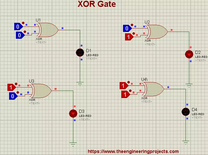
Hey pals, we hope you are doing well. In our previous lecture, we discussed the basic DLD Basic Logic Gates and simulated in Proteus. Today, we are going to discuss another logic gate called Exclusive OR Gate(XOR Gate). We will also design the XOR Gate in Proteus using the basic logic gates(i.e. AND, OR and NOT), discussed in the previous lecture.

In today's tutorial, we are going to focus on:

  1. What are Exclusive OR Gates
  2. Experimental Proof in Proteus ISIS.
  3. How Truth Table of Exclusive OR Gate is designed.
  4. How is its Timing Diagram?
  5. Circuit of Exclusive OR Gate in Proteus Simulation
  6. Applications of Exclusive OR Gates

Exclusive OR Gate(XOR Gate)

  • In the Exclusive OR Gate(XOR Gate), the output will be HIGH(1), only if the odd no. of inputs is HIGH(1) and at least one of the inputs is LOW. (it's a bit complex, will understand it in the next section)
  • The XOR Gate is denoted by a plus sign with a circle around it between the inputs i.e. A B.
  • XOR gate is designed by combining standard logic gates(i.e. AND, OR and NOT), but because of its extensive use in arithmetic operations and error detection, it's considered a standard logic gate.
  • The Truth Table of XOR Gate is given below:
A B
0 0 0
0 1 1
1 0 1
1 1 0
  • The XOR Gate symbol along with its representation and truth table is shown in the below figure:

Working Principle of XOR Gate

Its definition has two conditions in it:

  1. Odd no. of Inputs should be HIGH
  2. At least one of the inputs should be LOW

We have seen in the 2-Input XOR truth table, the output is HIGH in the 2nd and 3rd Rows, because these rows are fulfills both conditions i.e., we have an odd no of HIGH inputs(1 input is HIGH) and at least 1 LOW input(1 Input is LOW). While, in the 1st and 4th rows, both conditions are unfulfilled, thus getting LOW at the output.

Now, let's have a look at the truth table of the 3-input XOR Gate:

Image

Now it will get more clear, as you can see in the 4th row, we have 1 HIGH Input and 2 LOW Inputs, thus both conditions are fulfilled and we are getting HIGH at the OUTPUT. But in the 7th row, 2 Inputs are HIGH and 1 is LOW, although the 2nd condition is fulfilled i.e. we have at least 1 LOW input but the first condition is unfulfilled i.e. we have even no of HIGH Inputs. That's why we are getting LOW at the output. I hope now it gets clear.

Mathematical Representation of XOR

Now let's understand the output of the XOR gate mathematically. XOR gate is used in arithmetic calculations because it adds the inputs and gets the carry.

Here's the mathematical calculation of XOR truth table:

 0+0=0

0+1=1

1+0=1

1+1=0 (Carry)

Here's the Proteus demonstration of the XOR truth table:

Design XOR Gate with Standard Logic Gates

Now, we are going to design an XOR gate using the basic logic gates i.e. AND, OR and NOT. The formula for XOR Gate is as follows:

Y = A.(B)' + (A)'.B

As you can see in the above equation, we can get an XOR output(Y) by applying 3 logic gates i.e. AND, OR and NOT, on the inputs(A and B).

Let's verify this equation by putting values from the XOR truth table:

For 1st Row:

=0.(0)'+(0)'.0

=0.1+1.0

=0+0

=0

For 2nd Row:

Now, A=0, B=1:

=0.(1)'+(0)'.1

=0.0+1.1

=0+1

=1

For 3rd Row:

Consider A=1, B=0:

=1.(0)'+(1)'.0

=0.1+0.0

=1+0

=1

For 4th Row:

At last, check the expression when A=1, B=1:

=1.(1)'+(1)'.1

=1.0+0.1

=0+0

=0

So, now let's design this equation for the XOR Gate in the Proteus software. Let's get started:

Proteus Simulation of XOR Gate

As we have seen in the previous section, we need to implement this equation in the Proteus software:

Y = A.(B)' + (A)'.B

So, open your Proteus software and get these components from the Proteus library:

Material Required:

  1. AND Gate
  2. OR Gate
  3. NOT Gate
  4. Logic Toggle
  5. LED

Circuit Diagram of XOR Gate:

Here's the circuit diagram of the XOR Gate in Proteus using the standard logic gates i.e. AND, OR and NOT:

  • As you can see in the above figure, the upper AND gate is implementing the first part of the equation i.e. A.(B)' and the second AND gate is implementing the second part i.e. (A)'.B
  • NOT Gate in inversing the inputs, placed at the inputs of AND Gates.
  • Finally, we placed an OR gate to add the outputs from both AND gates so that we could complete the equation i.e. A.(B)' + (A)'.B 
  • Finally, we placed an LED at the output.

Applications of XOR Gate

XOR Gate is used in many circuits as:
  1. We use XOR Gate in Half Adder.
  2. It is used in the circuit of Controlled inverters.
  3. XOR is also used in comparators.
  4. Subtractor is the application of XOR Gate.
  5. The parity checker is made through XOR Gate.
  6. XOR is used in the Arithmetic Logic Circuits.
  7. Circuit of Binary to Grey and vice versa.
Today, we discussed the Exclusive OR Gate in detail. We have also designed the simulation of XOR Gate in PRoteus software with the help of basic logic gates i.e. AND, OR and NOT gates. That's all for today. Take care!!!

XNOR Gate with Truth Table in Proteus ISIS

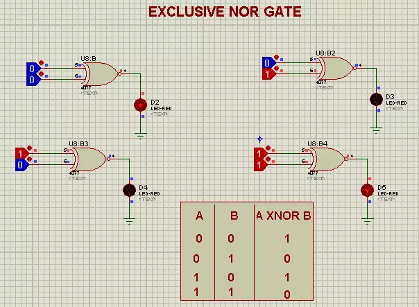
Hello Mentees!, I hope you have a productive day. Welcome to The Engineering Projects. In the previous lecture, we discussed the XOR Logic Gate and designed its circuit using basic logic gates i.e. AND, OR and NOT. Today, I am going to explain another Logic Gate named XNOR Gate in detail.

We are going to discuss these concepts in today's lecture:

  1. What are Exclusive NOR Gates
  2. Experimental Proof in Proteus ISIS.
  3. How Truth Table of Exclusive NOR Gate is designed.
  4. How is its Timing Diagram?
  5. Circuit of Exclusive NOR Gate in Proteus Simulation
  6. Applications of Exclusive NOR Gates

XNOR Gate

  • The exclusive NOR Gate(also called XNOR Gate) simply inverts the output of the XOR Gate(we discussed in the last lecture).
  • So, if we simply place a NOT Gate in front of the XOR Gate, we will get the XNOR Gate.
  • The XNOR Gate is denoted by a plus sign with a circle around it between the inputs and a collective Complement or a Bar on the Expression.
  • The symbolic representation of XNOR along with symbol and expression is shown in the below figure:
  • The Truth Table of XNOR Gate is given next:
A B Y
0 0 1
0 1 0
1 0 0
1 1 1

Mathematical Expression of XNOR Gate

The XNOR Gate with 2-inputs(A and B) and 1 Output(Z) is represented by the following mathematical expression:

Z = (A)'.(B)' + A.B

So, we will need AND, OR and NOT logical gates to implement XNOR Gate. Let's first verify this equation by applying the truth table.

For 1st Row:

=(0)'.(0)'+0.0

=1.1+0.0

=1+0

=1

For 2nd Row:

Now, A=0, B=1

=(0)'.(1)'+0.1

=1.0+0.1

=0+0

=0

For 3rd Row:

Consider A=1, B=0:

=(1)'.(0)'+1.0

=0.1+1.0

=0+0

=0

For 4th Row:

Lastly, A=1, B=1:

=(1)'.(1)'+1.1

=0.0+1.1

=0+1

=1

Hence in accordance with the above discussion, let's design the circuit of the XNOR Gate in the Proteus software:

Proteus Simulation OF XNOR Gate

Now let's design the Proteus Simulation of the XNOR gate. We simply need to implement the mathematical expression of XNOR Gate, discussed in the last section.

Material Required:

  1. AND Gate
  2. OR Gate
  3. NOT Gate
  4. Logic Toggle
  5. LED

Circuit Diagram of XNOR Gate:

First of all, we will design the below circuit in Proteus:

Image

As you can see in the above figure, the first AND Gate is getting the inverted inputs and the second AND Gate is provided with simple inputs. Finally, the output of both AND gates is passed through the OR Gate and we got our XNOR output. I have placed an LED at the output to visualize it.

Applications of XNOR Gate

XOR Gate is used in many circuits as:
  1. We use XOR Gate in digital circuits.
  2. It is used in error-detecting Circuits.
  3. XOR is also used in Arithmetic Circuits.
  4. Encryption Circuits is the application of XNOR Gate.
  5. The combinational circuit is made through XNOR Gate.
  6. XNOR is used in sequential Circuits.
  7. Circuit of Binary to Grey and vice versa.
Today we saw discussed the Exclusive NOR Gate(XNOR Gate) in detail. We have also designed its simulation using AND, OR and NOT logic gates. Till the next tutorial, take care!!!

4-Bit Full Adder using Logic Gates in Proteus

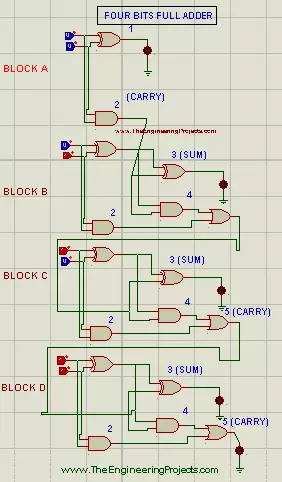
Hi Learners! I hope you are having a productive Day. Welcome from the Team of The Engineering Projects. The digital logic circuit that we are learning today is 4-Bit Full Adder. In our previous tutorial, we designed 2-Bit Full Adder using Logic Gates in Proteus software. Today, we are going to design & simulate 4-Bit Full Adder using Logic Gates in Proteus.

We will discuss the following topics in today's lecture:

  1. What is Adder?
  2. What is Full Adder?
  3. Working Principle of 4-bit Full Adder.
  4. Simulation of four-bit full Adder in Proteus ISIS.

What is Adder?

Let's recall the Adder Definition from our previous lectures:

  • Adders are Digital Logical Circuits, specially designed to add two or more binary numbers or bits.

In the world of electronics, adders are used to add bits. The computer system depends upon the flow of bits and the computation of bits. Adders take the input in the form of bits and perform the addition, according to the type of Adder used. Basically, we divide the adders into two types:

  1. Half Adder.
  2. Full Adder.

We have discussed both Half Adder & Full Adder in detail in our previous lectures. Yet we have to recall the full adder's introduction:

What is Full Adder?

"Full Adders are the Digital Logic Circuits used to add three input bits and generate two outputs i.e. the Sum and the resultant Carry."

We further classify the Full Adder into two main types:

  1. 2-bit Full Adder.
  2. 4-bit Full Adder.

4-bit Full Adder

As the name implies, a four-bit full adder is used to add four sets of input bits. The definition of a 4-bit Full adder is as follows:

  • "A 4-bit Full Adder is designed to generate a 4-bit Sum and is designed by combining four 2-bit Full Adders and as a result shows the Four bits output along with the Carry Bit."

The Circuit of the Four-bit Full Adder consists of the XOR Gate, AND Gate and OR Gate. Let's have a quick recap of these Gates.

XOR Gate

A XOR Gate, is a two input Logical Circuit that give the output HIGH only when the inputs have the values alternating of each other. Or else, it is LOW.

AND Gate

AND Gate is the a logical Circuit that gives the Output HIGH only when its both inputs are HIGH, otherwise the output is LOW.

OR Gate

The OR Gate is a logical Circuit with the working such that when on of the Input is HIGH, the value of the Output is also HIGH.

Working Principle of 4-bit Full Adder

The Four Bit Full Adder works in an interesting manner. The XOR Gates are responsible for the addition of input bits. In order to get the full addition circuit we attach two AND gates with the circuit in such a way that the result of addition connects the OR Gate and we get the carry.

In the designing of circuit, we simply make a small circuit of AND Gate and XOR Gate. Then we design a Circuit of two bits Full Adder. The cynosure of the circuit is, we'll copy the block and arrange four blocks in a way that the output carry of the block becomes the input carry of the next. This cycle will continue and at the  fourth block we get the resultant carry of whole calculation. we can input only one carry of our will at the Block A.

Practical performance of 4-Bit Full Adder

If you wish to stimulate the Four bits full adder in Proteus then follow the simple steps given below. We'll make our circuit according to the Functional Diagram given before.
  • Begin Your Proteus Software.
  • Get the required material.

Required Devices

  1. XOR Gate
  2. AND Gate
  3. OR Gate
  4. Logic Toggle
  5. LED
  6. Ground Terminal
  • Push the "P" button presented at left area of the screen.
  • Select first four elements from the Library by mere writing there names one after the other.
  • Get  a XOR Gate and one AND Gate.
  • Connect the Logic Toggles with each input of XOR Gate.
  • Connect an LED with the end of the XOR Gate.
  • Go to Terminal Mode and get the ground terminal to attach the Ground Terminal with LED.
  • Drag and drop two XOR Gates, two AND Gates and one OR Gate and arrange them at the working area one after the other according to the image given below:
  • Attach Logic Toggle with each input of switch 1.
  • Get the LED and join it with the output of switch 3.
  • Click the left button of mouse> go to Terminals> Ground Terminal.
  • Place the ground Terminal just below the LED.
  • Join all the components according to the images given below;
 
  • Select the whole block left click>drag and drop the required area. It will create a doted square around the circuit.
  • Right Click> copy block.
  • Right click the mouse and paste the block with the same procedure.
  • Repeat the Pasting Process one time more and paste the circuit copy just one below the other.
  • Connect the each output carry switch with the input of the next.
  • Grab the Logic Toggle from the Pick Library and join it with the input carry wire of the first block.
  • Change the input values by the mean of Logic Toggles and check the working.

Working Example of 4-bit Full Adder in Proteus

You can test the circuit with an example. Question: We have two numbers 1100 and 1010. Find the resultant through four bits Full Adder. Answer: Let A=1100 B=1010

Logic about For bit Full Adder

The 1st Logic Toggle of each XOR 1 switch is called A bit. The 2nd Logic Toggle of each XOR 1 represents the B bit. Turning of LED means the HIGH (1) and vise versa. We start to input from down to up and the output as well. Hence start the observation from block D to A.  For the Question, the circuit should be set as: Hence we got the answer that is:
A 1 1 0 0
B 1 0 1 0
Result (1 carry)0 1 1 0
Consequently, we made a Four bit Full Adder. Stay tuned for other Logical Circuits.

2-Bit Full Adder using Logic Gates in Proteus

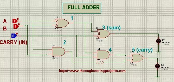
Hello Learners! I hope you are doing great. Welcome to The Engineering Projects. In our previous lecture, we discussed How to design Half Adder with Universal Gates. In today's tutorial, we are going to design Full Adder with Logical Gates.

In today's tutorial, we will learn the complete information about:

  1. What is Adder?
  2. What is Full Adder?
  3. How is the Truth Table of Full Adder?
  4. How can we design Full Adder in Proteus ISIS?
  5. What are the uses of Full Adder?

What is Adder?

Recalling from our previous lectures:

  • The Adders are simple Logical Circuits that take the bits in as the input, sum the bits together and generate the sum and the carry at the output.
  • Adders are present in computer architecture, mainly to control the addressing of the Arithmetic Logic Unit(ALU).

We classify the Adders into two types:

  1. Half Adder.
  2. Full Adder.

We have discussed half Adder in detail in our previous two lectures. Today we'll stress the Full Adder:

What is Full Adder?

There are two types of Full Adders:

We define the Full Adder as:

  •  A Full Adders is a simple Logical Circuit, that takes 3 inputs(1-bit each) and generates two outputs i.e. the Sum(1-bit) and the Carry(1-Bit).
  • A Full Adder takes 2 inputs A and B, while the third input is actually the Carry Input.
  • We have seen in the Half Adder that we took 2 inputs and calculated the Sum and the Carry but we have no way of adding that Carry back into the Sum.
  • This problem is solved by the Full Adder, which takes the Carry and adds it in the Sum to get a final Sum.
  • That's why, we can use multiple Full Adders in series to add any amount of Bits.
  • For example, we can serially attach 8 Full Adders to add 8 Bits of data(1-byte).

The Full Adder plays an important role in computer hardware calculations i.e. ALU control, register addressing etc. Here's a simple 2-Bit Full Adder Circuit using Logic Gates:

Truth Table of 2-bit Full Adder

As discussed above, there are three inputs and two outputs present in Full Adder. Therefore, the Truth Table of Full Adder will have 5 columns in total:

The input combinations of the Truth Tables are followed through the formula:

Numbers of Combinations= 2^n

where n is the number of inputs. In our case,

n=3

hence,

Numbers of Combinations=8

We start the truth table from zero bit. The right most input has the alternative inputs after each combination. The middle contains the alternative bits after two combinations. By the same token the left most changes the input bit after four combinations.

The Truth Table of Full Adder looks like this:

A B Cin Sum
C0
0 0 0 0 0
0 0 1 1 0
0 1 0 1 0
0 1 1 0 1
1 0 0 1 0
1 0 1 0  1
1 1 0 0 1
1 1 1 1 1
Carry+A+B Sum Carry out

Simulation of Full Adder in Proteus ISIS

To design a Full Adder in Proteus, get these components from the library:

Components Required

  1. XOR Gate
  2. AND Gate
  3. OR Gate
  4. Logic Toggle
  5. LED
  6. Ground Terminal
  • Get the first five components from the Pick Library through the "P" button.
  • As shown in the below figure, I have placed the 5 Logic Gates in our Proteus workspace.
  • We have 2 XOR Gates at the top, after that we have 2 AND Gates and finally an OR Gate at the end.
  • The circuit should look like this:
  • Now, connect two Logic Toggles with the inputs of Logic Gate 1.
  • Connect one Logic Toggle with the 2nd input of Logic Gate 3.
  • Attach the LED with the Gate 3 output and ground the LED with Ground Terminal present in "Terminal Mode" on the leftmost bar of the screen.
  • Repeat the above step for Logic Gate 5.
  • Connect all the Logic Gates according to the diagram given next:
  • Change the Input bits and record your own truth table.
  • To understand the working better, we'll design a Truth Table that describes the output of each Logic Gate.
Input Output
A B Cin Gate1
Gate2 Gate4 Gate3(Sum) Gate5 C0
0 0 0 0 0 0 0 0
0 0 1 1 0 0 1 0
0 1 0 1 0 0 1 0
0 1 1 0 1 0 0 1
1 0 0 0 0 0 1 0
1 0 1 1 0 1 0 1
1 1 0 1 0 1 0 1
1 1 1 0 1 0 1 1
Carry+A+B Sum Carry out

Truss, we got a Full Adder circuit through which we can make the calculations.

Uses of Full Adder

  1. Full adders are paramount for the on-chip Libraries.
  2. They are used in computers for table indices.
  3. They are used by the processor to add the addresses.
  4. Full adders are used in Arithmetic Logic Unit.
  5. Full Adders are used in the Computer for the series calculations. For this purpose, they may be connected in the way given next in the image. Observe it from bottom to top.[TEPImg6]
  6. It can be designed so, that we can input eight bits together that collectively work as a byte.
So, that was all for today. We discussed What are Adders? What are Full Adders? Truth Table of Full Adder and how can we design Full adder in the Proteus software. I hope this article was useful. In our next lecture, we will discuss 4-Bit Full Adders in detail. Thanks for reading.

What are DLD Logic Gates? Symbol | Truth Table | Simulation

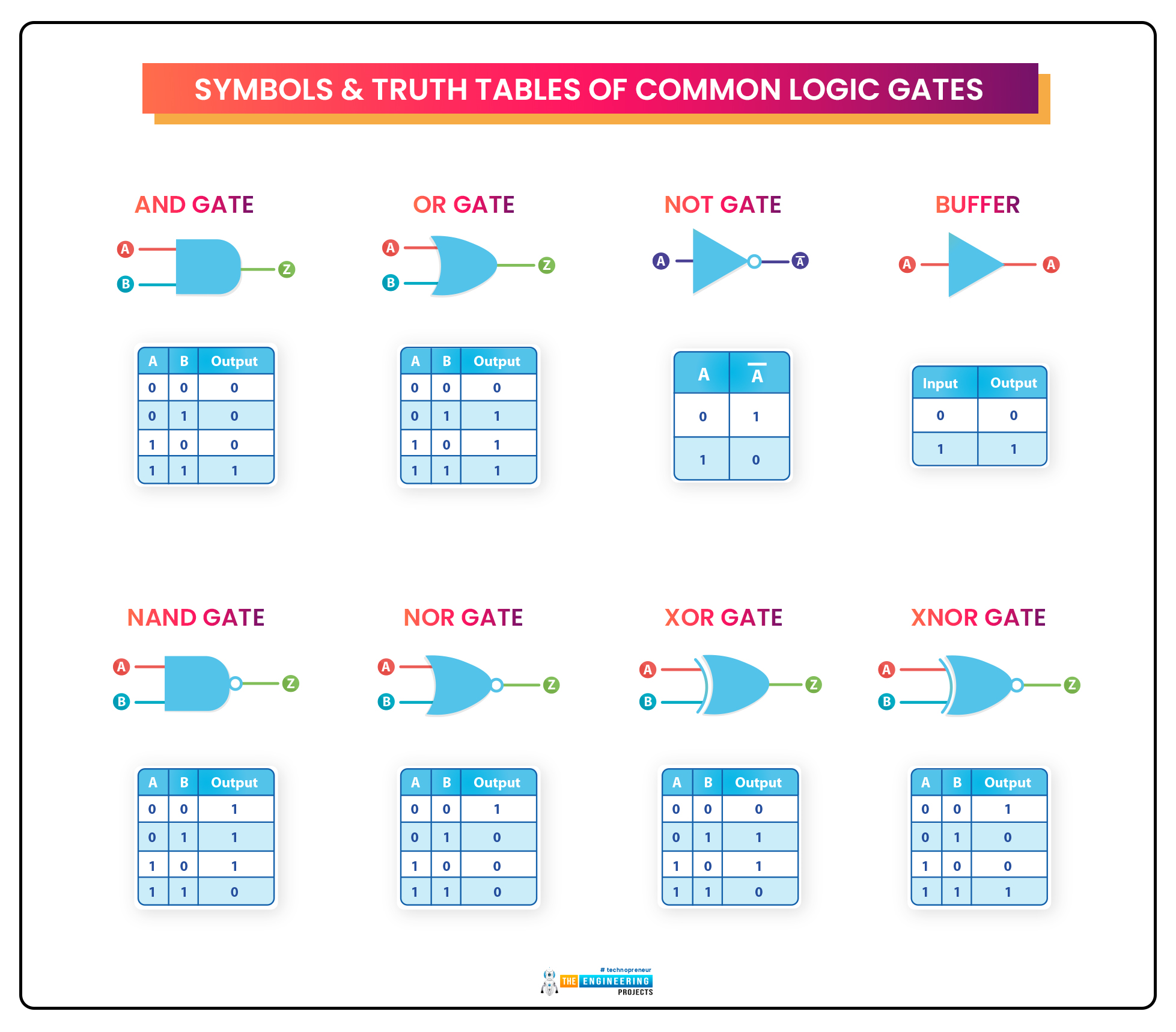
Hello Mentees! I hope you all are doing well. In today's article, we'll learn about the very basic pillar of Digital Logic Circuits i.e. Logic Gates. As we know, the digital world depends on Boolean digits either 0 or 1. So, there's always a need to perform different operations on these boolean numbers i.e. addition, subtraction, multiplication, shifting etc. In order to perform these operations on the binary signals, we use Digital Logic Gates in DLD circuits.

So, let's have a look at What is a Logic Gate:

What is a Logic Gate?

  • Logic Gates are designed to perform a specified operation(i.e. addition, bit shift etc.) on the input signals and generate the output signal.
  • For example, a simple NOT gate takes a single binary input and returns its inverse in the output, i.e.
    • If Input is 0, the Output will be 1.
    • If Input is 1, the Output will be 0.
  • We can design Logic gates using basic electronic components i.e. resistor, diode, transistor, etc. However, in order to design gates for commercial use, two main manufacturing technologies are used, i.e:
  • TTL(Transistor-Transistor Logic): TTL Logic gates use NPN & PNP Bipolar Junction Transistors in their circuitry i.e. 7400 series.
  • CMOS(Complementary Metal Oxide Silicon): CMOS Logic Gates use MOSFET or JFET transistors(i.e. 4000 series)yea ri and are quite popular because of their ultra-quick response.

Symbolic Representation

  • Each Logic gate is assigned a symbol for its representation, which simplifies the designing of their circuit diagrams.
  • The symbolic representation of 4 basic logic gates is as follows:

Truth Table

  • Every logic gate has a truth table(also called a logical table), used to provide the output states for all the possible combinations/conditions of its inputs.
  • It's a convention to write the outputs in the right-side columns and the inputs in the left-side columns.
  • The truth table of NOT Gate(used to inverse input), is shown in the below figure:
Input
Output
0 1
1
0
  • As you can see in the above figure, the table has 2 rows in total giving us all the possible input conditions.
  • The number of rows in a truth table depends on the number of inputs used. The formula is, if we have "n" number of inputs in a logic gate, its truth table will have 2n rows in total. So, if we have 2 inputs, the rows of its truth table will be 22 = 4.

Truth tables are useful in Boolean and mathematical operations as the relationship between the Input and Output can be understood at a glance.

Now let's have a look at the Circuit Designing of Logic Gates:

Logic Gates Circuit Designing

As we discussed earlier, different Manufacturing Techniques are used to design logic gates. These techniques decide the characteristics of the logic gates i.e. response time, noise immunity, voltage level for logic shifting etc. We can use simple electronic components i.e. diode, transistor, resistor etc. to design logic gates. The normal practices for designing logic gates with simple electronic components are:

  • RTL (Resistor-Transistor Logic)
  • DTL ( Diode-Transistor Logic)
  • ECL (Emitter-Coupled Logic)
  • DRL (Diode-Resistor Logic)

Such logic gates are quite simple in designing and normally have quite low response time and may also provide false output because of noise. So, in order to overcome these issues, these two manufacturing techniques are used:

  • TTL(Transistor-Transistor logic)
  • CMOS(Complimentary Metal oxide Semiconductors)

Simple NPN and PNP transistors are used in TTL logic gates and thus have better response time as compared to basic logic gates. In the CMOS technique, MOSFET and FET are used to control the logic and thus provide the best response time and are quite immune to noise. So, among all these manufacturing techniques, CMOS is considered the most popular technique for logic gate designing.

Logic Gates Designing with Basic Components

Here is an example of an AND Gate design with a Diode-Resistor Logic(DRL) and a NAND gate designed with Diode-Transistor Logic (DTL):

As you can see in the above figure, these circuits are quite easy to design, as simply using diodes, resistors, and transistors. But these circuits are not used in commercial ICs because of their high power loss(pull-up resistor) and gate delay(propagation delay). That's why, CMOS and TTL are considered the better option to design digital logic gates.

TTL Logic Gates

In TTL Logic Gates, NPN and PNP transistors are used for designing logic gates. The ideal TTL logic gate is the one that gives the LOW(0) Logic at 0V and HIGH(1) Logic at 5V. In a real TTL Logic Gate, the logic will be considered LOW(0), if the voltage level lies between 0-0.8V and the logic will be considered HIGH(1), if the voltage level is in the range of 2-5V. The voltage level between 0.8-2V is considered a "no man's land" and normally external pull-up or pull-down resistors are used to avoid this region. Examples of TTL Logic Gates ICs are 74Lxx, 74LSxx, 74ALSxx, 74HCxx, 74HCTxx, 74ACTxx etc. The switching voltage varies from group to group according to their internal structure and material used. 

CMOS Logic Gates

In CMOS Logic Gates, FET(Field Effect Transistor) and MOSFET are used to design the logic gates. CMOS logic gates provide a LOW(0) logic, if its voltage is in the range of 0-1.5V and it will give HIGH(1) logic, if it's in the range of 3-18V. The below table shows the voltage levels of both TTL and CMOS logic Gates:

Logic Gates
LOW(0)
HIGH(1)
TTL
0-0.8V
2-5V
CMOS
0-1.5V
3-18V

Now, let's have a look at the Types of Logic Gates:

Types of Logic Gates

  • There are numerous types of Logic gates available based on the quantity of input/output channels and the type of logic to be applied.
  • Based on the specified logic, gates are divided into 3 basic types, i.e.
    1. AND Gate.
    2. OR Gate.
    3. NOT Gate.
  • These 3 basic gates are the building blocks of all advanced logic gates. So, we can design any advance logic gate with these 3 basic logic gates.
  • The most commonly used Advance Logic Gates are:
    1. NAND Gate.
    2. NOR Gate.
    3. XOR Gate.
    4. XNOR Gate.
  • The above-mentioned 7 logic gates are the most commonly used ones. Following logic gates are not that common but are in practice:
    • MIN(Minimum) Logic Gate.
    • MAX(Maximum) Logic Gate.
    • INH(Inhibit) Logic Gate.
    • MAJ(Majority) Logic Gate.
    • IMP(IMPLY) Logic Gate.

It's quite difficult to cover all these gates in a single lecture. So, we will only discuss the basic 7 gates i.e. AND, OR, NOT, NAND, NOR, XOR and XNOR. Today, we will have a brief overview of these 7 logic gates but in the upcoming lectures, we will cover each one of these individually in full detail. Here are the symbols of few logic gates:

So, let's get started:

AND Logic Gate

  • AND Gate is a basic logic gate and gives  HIGH output, when all of its Inputs are HIGH and generates LOW output, if any of its Inputs got LOW.
  • The AND Gate performs the Logical conjunction. We denote it with the DOT between the inputs i.e. A.B = Y where A & B are the inputs and Z is the output.
  • The Inputs in AND Gate is always more than one i.e. Inputs >= 2 and it will always generate a single output.
  • The logical symbol of the AND gate is shown in the below figure:

Truth Table:

  • Here's the truth table of AND gate in tabular form:
A B A.B
0 0 0
0 1 0
1 0 0
1 1 1

As you can see in the truth table of AND Gate, the Output is 1 only when both of its inputs are 1, otherwise, it's 0.

Proteus Simulation of AND Gate

Proteus has an AND Gate component in its components library. We are going to use it to verify the truth table of AND Gate. We will use the following components for designing this AND Gate Simulation:

  1. AND Gate
  2. LED
  3. Logic Toggle
  4. Ground Terminal

Here's the Proteus simulation of all possible states of the AND Gate with 2-inputs:

  • I have placed a Logic State at the inputs of the AND gate and an LED at the output.
  • The LED glows only when both of its Inputs are 1(HIGH).

OR Gate

  • OR gate performs the Disjunction Logic on the inputs i.e. The output will be 1(HIGH), if any of its Inputs is 1(HIGH) and the output will be 0(LOW), if all of its Inputs are 0(LOW).
  • OR Gate is denoted by a plus sign "+" between the inputs i.e. A+B = Y, where A & B are the inputs and Y is the output.
  • Identical to AND Gate, OR Gate also has a minimum of two inputs and only one output.
  • The OR Gate Symbol is shown in the below figure:

Truth Table:

  • Here's the truth table for the OR Gate:
A B A+B
0 0 0
0 1 1
1 0 1
1 1 1

In the case of OR Gate, the output is LOW, only when all of its inputs are LOW, otherwise its HIGH.

Proteus Simulation of OR Gate

  • The simulation is quite the same as that of the AND gate, we simply replace the AND Gate with OR Gate, present in the Proteus components library.
  • The below figure shows that the output LED is OFF, only when both inputs of OR gate are LOW.

NOT Gate

  • In Logic Circuits, the NOT Gate performs the inversion.
  • This is a unary logic Gate that implies it has only one input and a single output.
  • The output of NOT Gate is denoted by a Bar or Complement on the input symbol i.e. If the input is A, the output will be A'.
  • Here's the symbolic representation of NOT Gate:

Truth Table:

  • Here's the truth table of NOT gate, quite simple isn't it?
A B
0 1
1 0
 

Proteus Simulation of NOT Gate

  • Grab the NOT Gate from the Proteus components library.
  • Attach LED and logic toggle at output and input respectively.
  • Here are the results:

So, today we discussed the basic logic gates i.e. AND, OR and NOT Gate and simulated them in Proteus. In upcoming lectures, we'll use these gates to design advance gates and circuits. Take care!!!

What are Digital Latches? | SR-Latches | D-Latches

Hi mentees, we are here with a new tutorial. I hope you all are fine. So far, we have been designing combinational circuits i.e. Adder, Subtractor, Multiplexer etc. using logic gates. But from today onward, we will design sequential circuits using logic gates i.e. Latches, Flip Flops etc. Let's quickly recall what's the difference between combinational & Sequential Circuits:

Combinational Circuits:

  • Combinational circuits only use the current state of the input values to generate the output.
  • Examples of DLD Combinational Circuits are: Adders, Subtractors, Multiplexers etc.

Sequential Circuits

  • Sequential Circuits use both the current & previous states of the inputs to generate the output.
  • Examples of DLD Sequential Circuits are: Latches, Flip Flops, Timers, Counters etc.

Digital Memory Elements

Normally two types of memory elements are used in digital circuits to store binary data, named:

  • Latches
  • Flip Flops(We will cover in the next lecture)

As today's lecture is on Latches, so let's explore it:

What are Latches?

  • Latches are used in digital circuits as a memory element and are used to store/save the input states.

The two inputs of Latches are called "S" and "R" where S stands for SET and R stands for RESET. Due to inputs , latches can have four unique combinations of the input. The output is denoted as "Q" and is totally dependent on the input Combination.

Nevertheless, another Output is also used in the circuit sometimes. this output is denoted as Q' and is read as Q bar, Complement of Q or bar Q  NOT Q because it is also written as:

One can have an idea that this output is the invert result of "Q" output and depends on the Q and successively to the inputs S and R.

Two types of circuits are possible in latches:

  1. Active high circuits.
  2. Active low circuits.
Both of them are same in the Components but are different due to the arrangement of the Components. Active high circuits: In this kind of the Circuit the inputs are grounded and therefore are LOW. Latch are triggered momentary high signal. Active Low Circuits: In this kind the inputs are LOW and the latches are triggered at high signals.

TYPES OF LATCHES

Latches are classified into two main types:
  1. SR Latches
  2. D Latches.
whereas, 1st two types are further subdivided into two categories:
  1. Simple
  2. Gated
All of theses types along with the implementations are shown in figure on right side.

Prior to start  DO YOU KNOW???????

  • Logic Probes are used to give input to the circuit. They can only give two types of inputs:
  1. High ( Denoted by 1)
  2. Low ( Denoted by 0)
  • By the same token, Logic toggle show the output. There are two types of output:
  1. High ( Denoted by 1)
  2. Low ( Denoted by 0)
  • NAND gate shows the output LOW ( or 0) only when both the inputs are HIGH.
  • NOT gate show is an inverter gate.
  • NOR gate shows the output HIGH ( or 1) only when both the inputs are HIGH.

Implementation of Latches in Proteus ISIS

For best understanding, we'll design each of the type and create the truth table. Devices Required:
  1. AND Gate
  2. NOT Gate
  3. Three input AND Gate
  4. Logic Toggle
  5. Logic Probe
  6. Clock
Procedure: All the Circuits follow almost same procedure. Even so, they are different in the Construction and the characteristics.

1. SR Latches in Proteus ISIS

  • Choose Two NOR Gates and fix them on the working area.
  • Examine the Circuit diagram and arrange the other required Components according to the Circuit diagram.
  • Truss all the Components by wires with the help of circuit diagram.
  • Pop the Play button and fill the truth table.
NOTE: You can also make this Circuit with NAND Gate. Examination: The SR latch ( SET/RESET) mainly change according to the change in the S line. that means, whenever the S is HIGH the Q ( output) is shown as HIGH and vise versa.  but when both the inputs (SET & RESET)  are HIGH then we seen that both the outputs are LOW. Q ( output ) is alway the inverse of Q'. Once we check all the Conditions we can assemble our own truth table. I have made a truth table that shows us the following result:
S R Q Q’
0 0 1 0
0 1 0 1
1 0 0 1
1 1 0 1
 

2. Gated SR Latch in Proteus ISIS


The SR latch are not Complete, hence the performance can be enhanced by the a process called "Gating" , and the resultant circuit is called Gated SR Circuit.
  • We add two Positive NOR gates at the input "S" and "R" that have inverted input using NOT Gates. In this way we can examine the Condition more clearly when both the inputs in SR gate were HIGH.
  • The circuit works well when we add a clock in the two inputs of the NOR gates.
The Circuit of Gated SR is shown next: When we test the Circuit's all conditions , the output have some difference. The output here shows us the difference.  During the LOW conditions of the Circuit the output shows us the error or Latch.
CLK S R Q Q’
0 X X LATCH LATCH
1 0 0 LATCH LATCH
1 0 1 0 1
1 1 0 1 0
1 1 1 1 0

3. D Latches in Proteus ISIS

D latch is a modification of the Gated SK Latch.
  • we add the NOT Gate in advance of the RESET (R) Input and we get the circuit that looks like this:
  Accordingly to the Picture, the D  and clock are now the inputs of the Circuit and we can notice the output at Q and Q'.
CLK D Q Q’
0 0 NO CHANGE NO CHANGE
0 1 NO CHANGE NO CHANGE
1 0 0 1
1 1 1 0

4. Gated D Latch in Proteus ISIS

This is another type of D Latch.
  • Connect the clock with the D input so that  we alter the D input. But with this change, we see the changes in the output as well.
Let's have a look on the Circuit of Gated D Latch:   when we change the D and test all the Condition, the resultant truth table is:
CLK D Q Q’
0 0 0 1
0 1 1 0
1 0 1 0
1 1 0 1
Hence today we learnt about the latches, some basic concepts and its types along with  practical implementation.
Syed Zain Nasir

I am Syed Zain Nasir, the founder of <a href=https://www.TheEngineeringProjects.com/>The Engineering Projects</a> (TEP). I am a programmer since 2009 before that I just search things, make small projects and now I am sharing my knowledge through this platform.I also work as a freelancer and did many projects related to programming and electrical circuitry. <a href=https://plus.google.com/+SyedZainNasir/>My Google Profile+</a>

Share
Published by
Syed Zain Nasir