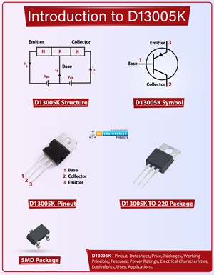
D13005K Datasheet, Pinout, Power Ratings, Equivalents & Applications

Introduction to d13005k, d13005k pinout, d13005k equivalents, d13005k power ratings, d13005k applications

Hello Everyone! Hope you’re well today. In today's tutorial, we will have a look at D13005K NPN Transistor. We will also study D13005K Datasheet, Pinout, Power Ratings, Equivalents & Applications. As its an NPN transistor, so major charge carriers are electrons. D13005K is mainly employed for switching and amplification purpose. Let's first recall NPN transistors: NPN transistor consists of 3 terminal, named as:

  • Emitter.
  • Collector.
  • Base.
If we provide voltage > 0.7V at base terminal, NPN transistor gets forward biased & starts conducting. If Base voltage < 0.7V, it remains reverse biased. So now let’s get started with D13005K NPN Transistor:

D13005K NPN Transistor

  • D13005K is a bipolar NPN transistor, mainly used for amplification and switching purposes.
  • It contains three layers where two n-doped layers surround one p-doped layer.
  • This device is made of silicon semiconductor material and comes in a TO-220 package.

Introduction to d13005k, d13005k pinout, d13005k equivalents, d13005k power ratings, d13005k applications

  • D13005K contains three terminals named base, collector, and emitter. All these terminals are different in terms of doping concentrations.
  • The small current at the base side is used to control the large current at the emitter and collector terminals.
  • These transistors are called bipolar because both electrons and holes play role in the conductivity inside the transistor.
  • Bipolar junction transistors are divided into two main types i.e. NPN and PNP transistors.
  • In the case of NPN transistors, electrons are the major charge carriers while holes are major charge carriers in PNP transistors.
  • The bipolar junction transistors are the current-controlled devices in contrast to MOSFETs that are voltage-controlled devices that come with terminals named: drain, source, and gate.
  • The NPN transistors are preferred over PNP transistors because the mobility of electrons is better than the mobility of holes.
  • While in the case of NPN transistors the current flows from the collector to emitter terminals and it flows from emitter to collector terminal in the case of PNP transistors.

D13005K Datasheet

It is wise to go through the datasheet of the device before incorporating this component into your electrical project. The datasheet comes with the main characteristics of the device. Click the link below to download the D13005K datasheet.

D13005K Pinout

  • The following figure shows the D13005K pinout:

The D13005K Pinout comes with three terminals named: 1: Base 2: Collector 3: Emitter Recall, all these terminals are different in terms of doping concentrations. The emitter side is highly doped and the collector side is lightly doped. The collector side is 10-times lightly doped than the base side. These terminals are used for the connection with the external circuits.


D13005K Working Principle

The working of this device starts from the base side. When voltage is applied at the base side, it will bias the device and as a result, current starts flowing from collector to emitter terminal. This bipolar device is not symmetrical in nature. And the different doping concentration of all three terminals is the reason these devices are not symmetrical. Which means if you exchange both emitter and collector terminals then these terminals will start operating in reverse active mode and it prevents these terminals to work in forward active mode.

D13005K Power Ratings

The following table shows the D13005K power ratings.
Absolute Maximum Ratings of D13005K
Pin No. Pin Description Pin Name
1 Collector-emitter voltage 400V
2 Collector-base voltage 700V
3 Base-emitter voltage 9V
4 Collector current 4A
5 Power dissipation 75W
6 Base current 2A
7 Operating and storage junction temperature range -55 to 150C
  • The junction temperature of this device is 150C and the storage temperature ranges from -55 to 150C.
  • The collector current is 4A which means this device can support load up to 4A.
  • The power dissipation is 75W which is the amount of energy this device releases during the working of this component.
  • Know that, don’t apply these ratings more than the required time, else they can affect device reliability.
  • The collector-emitter current is 400V and the collector-base voltage is 700V. And the emitter-base voltage is 9V which means this device will get biased when 9V is applied across the base and emitter terminals.

D13005K Applications

The following are the D13005K applications.
  • Used in voltage regulator circuits.
  • Used in electronic Ballasts.
  • Used in a common power amplifier.
  • Used in the high switching power supply.
  • Incorporated in modern electronic circuits.
  • Employed to support loads under 4A.
  • Used in high-frequency power transform.
  • Used in Bistable and Astable multivibrators circuit.
  • Used in energy-saving lights.

D13005K Physical Dimensions

The following diagram represents the D13005K physical dimensions. By checking those dimensions you can audit the space required for your component in the electrical project. That was all about the Introduction to D13005K. Feel free to share your thoughts around the content we share so we keep producing quality content customized to your exact needs and requirements. You can approach me in the section below if you need any assistance regarding this article. I’m happy and willing to help you the best way I can. Thank you for clicking this read.

Syed Zain Nasir

I am Syed Zain Nasir, the founder of <a href=https://www.TheEngineeringProjects.com/>The Engineering Projects</a> (TEP). I am a programmer since 2009 before that I just search things, make small projects and now I am sharing my knowledge through this platform.I also work as a freelancer and did many projects related to programming and electrical circuitry. <a href=https://plus.google.com/+SyedZainNasir/>My Google Profile+</a>

Share
Published by
Syed Zain Nasir