CA3130 MOSFET BiMOS Op-Amp Datasheet, Pinout, Features & Applications

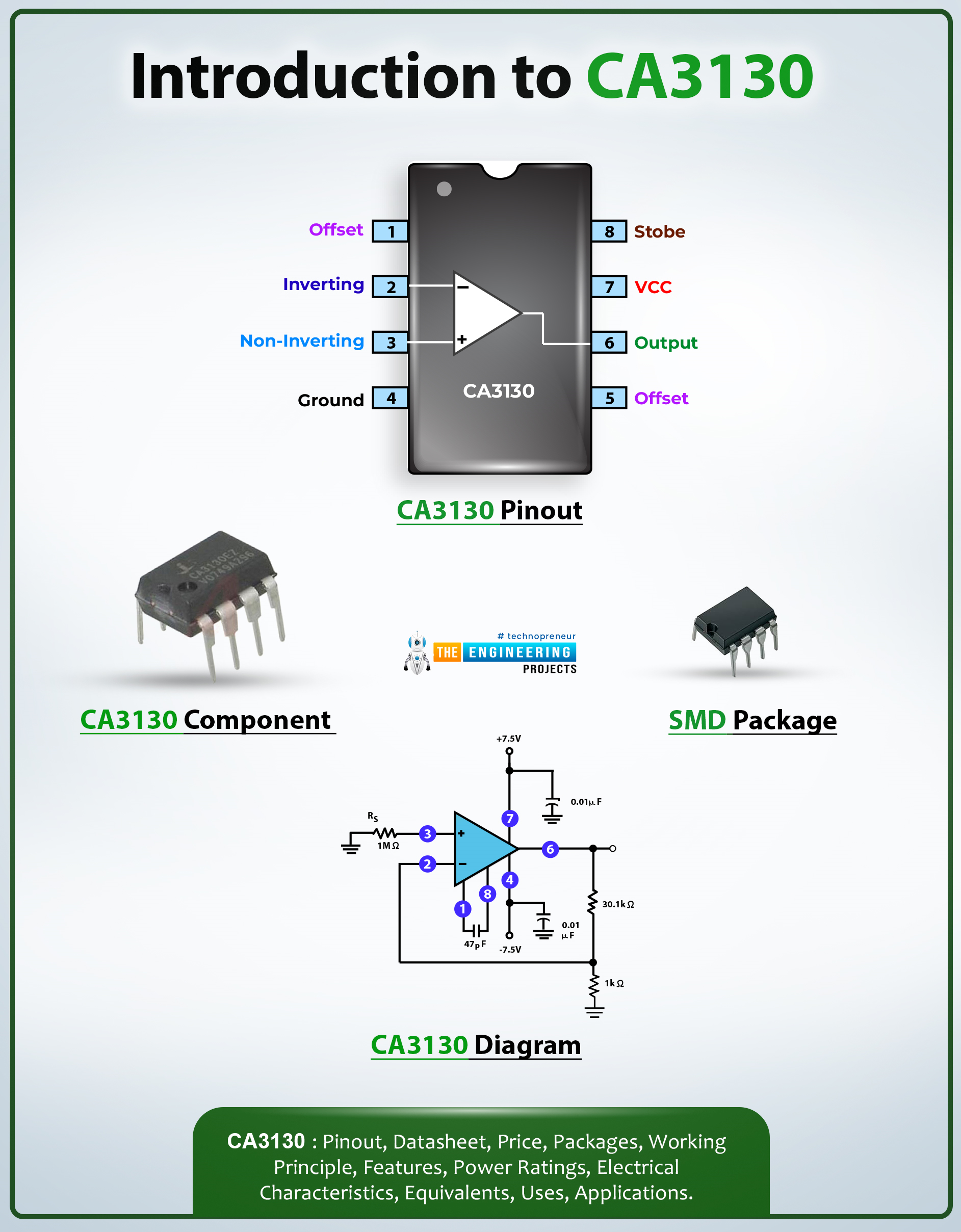
Hi Everyone! Hope you’re well today. I welcome you on board. In this post today, I’ll walk you through the Introduction to CA3130.

The CA3130 is a BiMOS Operational Amplifier that comes with MOSFET at the output. The term BiMOS suggests that it projects the advantage of both Bipolar and CMOS op-amp technology.

This IC comes with high bandwidth due to bipolar op-amps and consumes less current due to CMOS op-amp, making it a perfect fit for mobile jammers and voltage follower circuits.

I suggest you read this post all the way through as I’ll detail the complete Introduction to CA3130 covering datasheet, pinout, features, and applications. Let’s get started.

Introduction to CA3130

  • The CA3130 is a BiMOS Operational Amplifier that contains MOSFET at the output. This chip consumes less current and features high bandwidth.
  • This device has high input impedance due to MOSFETs which implies that when an output voltage of the sensor is connected to the inverting or non-inverting terminals of the op-amp, the output voltage from the sensor will not be disturbed since the op-amp will not act as a load to the sensor.

  • If you’re looking for a device with high input impedance, less power consumption, and high bandwidth, this chip might be the answer.
  • CA3130 is an eight-terminal electronic IC that comes with a Common Mode Rejection Ration (CMRR) of 80dB.
  • It is widely used in frequency generators and noise detectors.
  • The input terminal current of this device is 1mA and the supply current is 10mA.
  • The CA3130 features inverting and non-inverting pins like other op-amps. If the voltage at the non-inverting pin is high, the output across the inverting pin will be high, otherwise, it will be low.
  • Pins 1 & 5 are offset null pins used to nullify the offset produced when two input pins are combined. When the input pins of the op-amp are combined with each other, the voltage at the output should be zero. But no operational amplifier is ideally perfect. So when two inputs are combined together, it results in the offset. The offset null pins are used to null that effect.
  • Pin 8 is called Strobe that is mainly used to turn off the output stage. It is also employed for phase compensation in comparators.

CA3130 Datasheet

Before you incorporate this device into your electrical project, it’s wise to go through the datasheet of the device that features the main characteristics of the component. Click the link below and download the datasheet of CA3130.

CA3130 Pinout

The following figure shows the pinout diagram of CA3130. The following table shows the pin description of each pin incorporated on the chip.
Pin Description of CA3130
Pin No. Pin Description Pin Name
1,5 When the input pins of the op-amp are combined with each other, the voltage at the output should be zero. But no operational amplifier is ideally perfect. So when two inputs are combined together, it results in the offset. The offset null pins are used to null that effect. Offset Null Pins
2 The Inverting pin is also given a fixed voltage which is compared with the (IN+) Inverting Input (IN-)
3 The Non-Inverting Pin of the comparator gives a variable  voltage to compare Non-Inverting Input (IN+)
4 This pin is connected to the ground of the system (Negative voltage can also be used) Ground (VCC-)
6 This is the output pin of the op-amp Output
7 This VCC pin offers the operating voltage for the Op-Amp. For CA3130 it is up to +16V VCC+
8 Allows you to turn off the output stage Strobe

CA3130 Features

  • Op-amp laced with MOSFET at the output
  • Input Terminal current = 1mA
  • Wide power supply Range i.e. for single supply – 5V to 16V and for dual supply – ±2.5V to ±8V
  • Sink current Max. = 20mA
  • Source current Max. = 22mA
  • Output Voltage Max. = 13.3V
  • Supply current = 10mA
  • Common Mode Rejection Ration (CMRR) = 80dB

CA3130 Alternatives

The following are the alternatives to CA3130.
  • LM311
  • LM324
  • LM358
  • LM741
  • LM339
Check the pinout of the alternatives before incorporating them into your electrical project as the pinout of the alternatives might differ from the pinout of the CA3130.

CA3130 Applications

The CA3130 is used in the following applications.
  • Incorporated in DAC circuits
  • Used in voltage follower circuits
  • Employed in mobile jammers
  • Employed in Oscillator circuits
  • Used in frequency generator/distorter
  • Used in Peak Signal/Noise detectors

That’s all for today. Hope you find this article helpful. If you have any questions, you can pop your comment in the section below. I’d love to help you the best way I can. Feel free to share your valuable feedback and suggestions around the content we share so we keep coming back with quality content customized to your exact needs and requirements. Thank you for reading the article.

INA219 Current Sensor Module Datasheet, Pinout, Features & Applications

Hi Friends! Hope you’re well today. I welcome you on board. Today, I’ll walk you through the Introduction to INA219.

The INA219 is a current sensor module that incorporates the I2C protocol for submitting the data obtained through sensing current, voltage, and power. It is a bi-directional zero drift current/ power sensing module mainly used in digital multimeters and power profilers.

I suggest you read this post all the way through as I’ll detail the complete Introduction to INA219 covering datasheet, pinout, features, and applications. Let’s get started.

Introduction to INA219

  • INA219 is a current/power sensor module mainly employed to sense the power, voltage or current where up to 128 samples can be averaged together to get filtering in noisy environments. This data is then submitted to a microcontroller using the I2C bus.

  • This device features an I2C protocol mainly used to transmit data between devices. The I2C protocol comes with two wires SDA and SCL. The SDL is a serial data line that carries the data while SCL is a serial clock line that carries the clock signal and ensures the synchronization of data transfer over an I2C bus.
  • In the I2C protocol, one device acts like a master and the other as a slave. Using this communication protocol you can attach multiple slaves with a single master whereas you can also control single or multiple slave devices with multiple masters.
  • INA219 can be easily incorporated with microcontrollers and Arduino boards and with devices that come with an I2C bus interface.
  • It also contains a 2W 0.1 Ohms 1% rated shunt resistor mainly employed to fulfill the current measuring requirements.
  • This sensor module is a key part of the power monitoring systems. The power input of this device ranges from 3V to 5.5V and the target voltage is up to +26V.

INA219 Datasheet

It is better to go through the datasheet of the device before you embed this device into your electrical project. The datasheet features the main characteristics of the module. Click the link below to download the datasheet of INA219.

INA219 Pinout

The following figure shows the pinout diagram of INA219. The following table represents the pin description of each pin incorporated into the module.
Pin Description of INA219
Pin No. Pin Description Pin Name
1 Sensed Input line - VIN-
2 Sensed Input line + VIN+
3 Input voltage VCC
4 Connected to ground GND
5 Serial clock line that carries the clock signal SCL
6 Serial data line that contains the data SDA

INA219 Features

  • Contains 2C- or SMBus-compatible interface
  • Comes with up to +26V target voltage
  • Power Input Range = 3.0V-5.5V
  • Can Sense Bus Voltages ranging from 0 to 26 V
  • Up to 128 samples are averaged to get filtering in noisy environments.
  • Capable of up to ±3.2A current measurement, with ±0.8mA resolution
  • Contains ohm 1% 2W current sense resistor
  • Board Dimension = 0.8 x 0.9 inch (l x w x h)

INA219 Applications

  • Used in power monitoring systems
  • Employed in power profiler
  • Used in digital multimeter

That’s all for today. Hope you find this article helpful. If you’re unsure or have any questions, you can approach me in the section below. I’d love to help you the best way I can. Feel free to share your valuable feedback and suggestions around the content we share so we keep coming back with quality content customized to your exact needs and requirements. Thank you for reading the article.

FDV301N N-channel MOSFET Datasheet, Pinout, Features & Applications

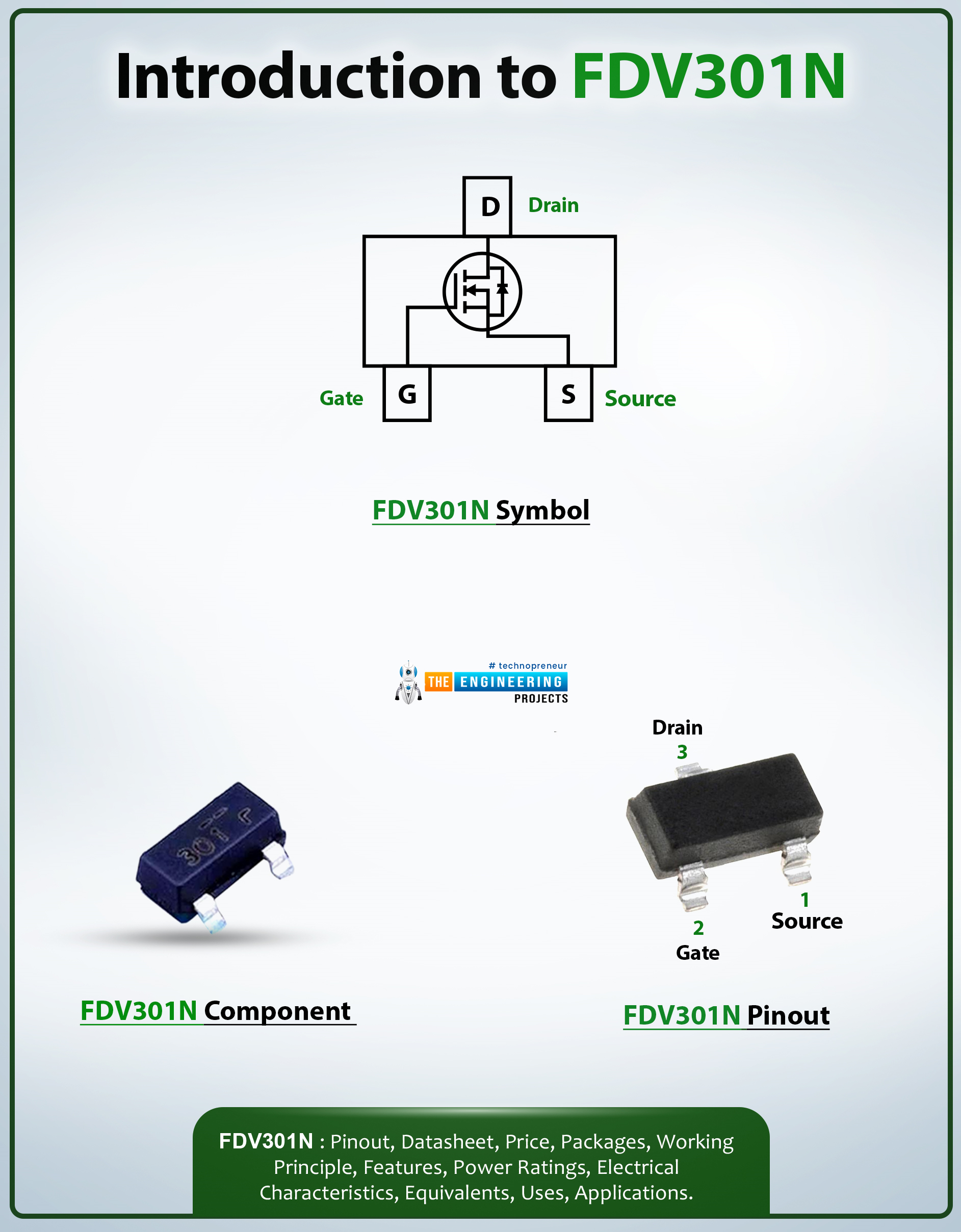
Hello Everyone! I welcome you on board. Happy to see you around. In this post today, I’ll walk you through the Introduction to FDB301N.

The FDV301N is an N-channel MOSFET using Fairchild's proprietary and high cell density, DMOS technology. The cell’s high density helps to minimize the on-state resistance. This device is mainly developed for low-voltage applications. This N-channel MOSFET replaces different digital transistors and provides different bias resistor values.

I suggest you read this post all the way through as I’ll detail the complete Introduction to FDV301N covering datasheet, pinout, features and applications. Let’s jump right in.

Introduction to FDV301N

  • The FDV301N is an N-channel MOSFET mainly used for switching and low-voltage applications.
  • It carries low on-state resistance and can be used in place of different transistors for a range of applications.

  • This device contains three terminals named gate, drain, and source. The source is the terminal from which electrons enter the channel and drain is the area where electrons leave the channel. While gate terminal is used for biasing the device.
  • The MOSFETs are mainly divided into two main types i.e. N-channel MOSFET and P-channel MOSFET. The N-channel MOSFETs carry electrons as major charge carriers and P-channel MOSFETs contain holes as the major charge carriers.
  • The movement of electrons is better than the movement of holes, making N-channel MOSFETs better than P-channel MOSFETs for a range of applications, especially for high-load applications.
  • The drain-source voltage of this device is 25V and gate-source voltage is 8V and maximum power dissipation is 0.35W. This is the amount of power it dissipates during the working of this device.

FDV301N Datasheet

It’s wise to go through the datasheet before you apply this component to your electrical project as using this datasheet you can get a hold of the main characteristics of the device. Click the link below to download the datasheet of FDV301N.

FDV301N Pinout

The following figure shows the pinout diagram of FDV301N. This chip comes with three terminals called source, gate, and drain.
Pin Description of FDV301N
Pin No. Pin Description Pin Name
1 Electrons enter the channel through the source terminal Source (S)
2 Used for biasing the device Gate (G)
3 Electrons leave the channel through the source terminal Drain (D)

FDV301N Features

The following are the main features of FDV301N.
  • The RDS (on-state resistance) is a resistance between drain and source terminal that is 5? at gate-source voltage VGS of 2.7V and it’s 4? at VGS of 4.5V.
  • The gate-source voltage (VGS-th) is 8V
  • Drain Source Voltage (VDS) is 25V
  • Continuous Drain Current (ID) is 220mA
  • Level gate drive requirements are very low, helping direct operation in 3V circuits.
  • The high-density cell process ensures low on-state resistance RDS (ON).
  • This device is reliable and rugged.
  • The operating and storage temperature range is -55C to 150C.
  • Comes in a compact industry-standard SOT-23 surface-mount package.

FDV301N Applications

This N-channel MOSFET chip is used in the following applications.
  • Incorporated in low voltage low current applications.
  • Employed as switching devices in electronic control units.
  • Used in automotive electronics.
  • Used as power converters in modern electric vehicles.
  • Used in servo motor control.

That’s all for today. Hope you’ve got a brief insight into the Introduction to FDV301N. If you have any query, you can share your comment in the section below, I’ll help you the best way I can. Feel free to share your valuable feedback and suggestions around the content we share so we keep producing quality content customized to your exact needs and requirements. Thank you for reading the article.

IRF520 MOSFET Datasheet, Pinout, Features & Applications

Hi Guys! Hope you’re well today. Happy to see you around. Today, I’ll walk you through the Introduction to IRF520.

The IRF520 is an N-channel power MOSFET mainly used for switching and amplification purposes. It comes with a breakdown voltage of around 100V and a low gate threshold voltage is 4V, making it an ideal pick for microcontroller applications.

I suggest you read this post all the way through as I’ll detail the complete Introduction to IRF520 covering datasheet, pinout, features, and applications. Let’s get started.

Introduction to IRF520 MOSFET

  • The IRF520 is an N-channel power MOSFET mainly used for switching and amplification purposes.
  • It comes with three terminals named: gate, source, and drain and is available in the TO-220 package.
  • It is important to note that the gate terminal is electrically insulated and contains no current and is normally called an Insulated Gate FET (IG-FET).

  • As it’s an N-channel MOSFET so here major charge carriers are electrons as opposed to P-channel MOSFET where major carriers are holes.
  • The movement of electrons is better than the movement of holes, making N-channel MOSFET better than P-channel MOSFET.
  • Due to better movement of electrons, N-channel MOSFETs with high loads remain cool while P-channel MOSFETs turn hot in the presence of high loads.
  • The major charge carriers i.e. electrons enter the channel through the source terminal while they exit the channel through the drain terminal. And the gate terminal controls the biasing of this MOSFET.
  • This N-channel MOSFET comes with low on-state resistance of around 0.27 ohm, allowing it to dissipate less energy as heat and consequently increasing the efficiency of the device.
  • IRF520 contains a low threshold voltage of around 4V which projects it can be turned on with 5V on the GPIO pins on the microcontroller.
  • This chip comes with a decent switching speed, making it an ideal pick for DC-DC converter circuits.
  • The continuous drain current (ID) of this device is 9.2A while the drain-to-source breakdown voltage is 100V. The Rise time is 30ns and the fall time is 20nS.

IRF520 Datasheet

Before you apply this component to your electrical project, it’s wise to scan through the datasheet of the component that features the main characteristics of the device. Click the link below to download the datasheet of IRF520.

IRF520 Pinout

The following figure shows the pinout diagram of IRF520 Mosfet. The IRF520 comes in three terminals named Gate, Drain, and Source.
Pin Description of IRF520
Pin No. Pin Description Pin Name
1 Used for biasing the device Gate
2 Electrons leave the channel through a drain terminal Drain
3 Electrons enter the channel through the source terminal Source

IRF520 Features

The following are the main features of IRF520 mosfet.
  • N-Channel Power MOSFET
  • Continuous Drain Current (ID) = 9.2A
  • Drain to Source Breakdown Voltage = 100V
  • Rise time is 30ns and the fall time is 20nS.
  • Drain Source Resistance (RDS) = 0.27 Ohms (also known as on-state resistance)
  • Since it contains low threshold voltage, it is commonly employed with Arduino applications.
  • Gate threshold voltage (VGS-th) = 4V (max)
  • Available Package = TO-220 package

IRF520 Applications

The following are the main applications of this device.
  • Employed to control the speed of motors
  • Used in converters or Inverter circuits
  • Used in high power devices
  • Incorporated in high-speed switching applications
  • Used in LED dimmers or flashers

That’s all for today. Hope you’ve got a brief insight into Introduction to IRF520 mosfet. If you’re unsure or have any questions, you can approach me in the section below. I’d love to help you the best way I can. Feel free to share your valuable feedback and suggestions around the content we share so we keep coming back with quality content customized to your exact needs and requirements. Thank you for reading the article.

BSS138 MOSFET Datasheet, Pinout, Features & Applications

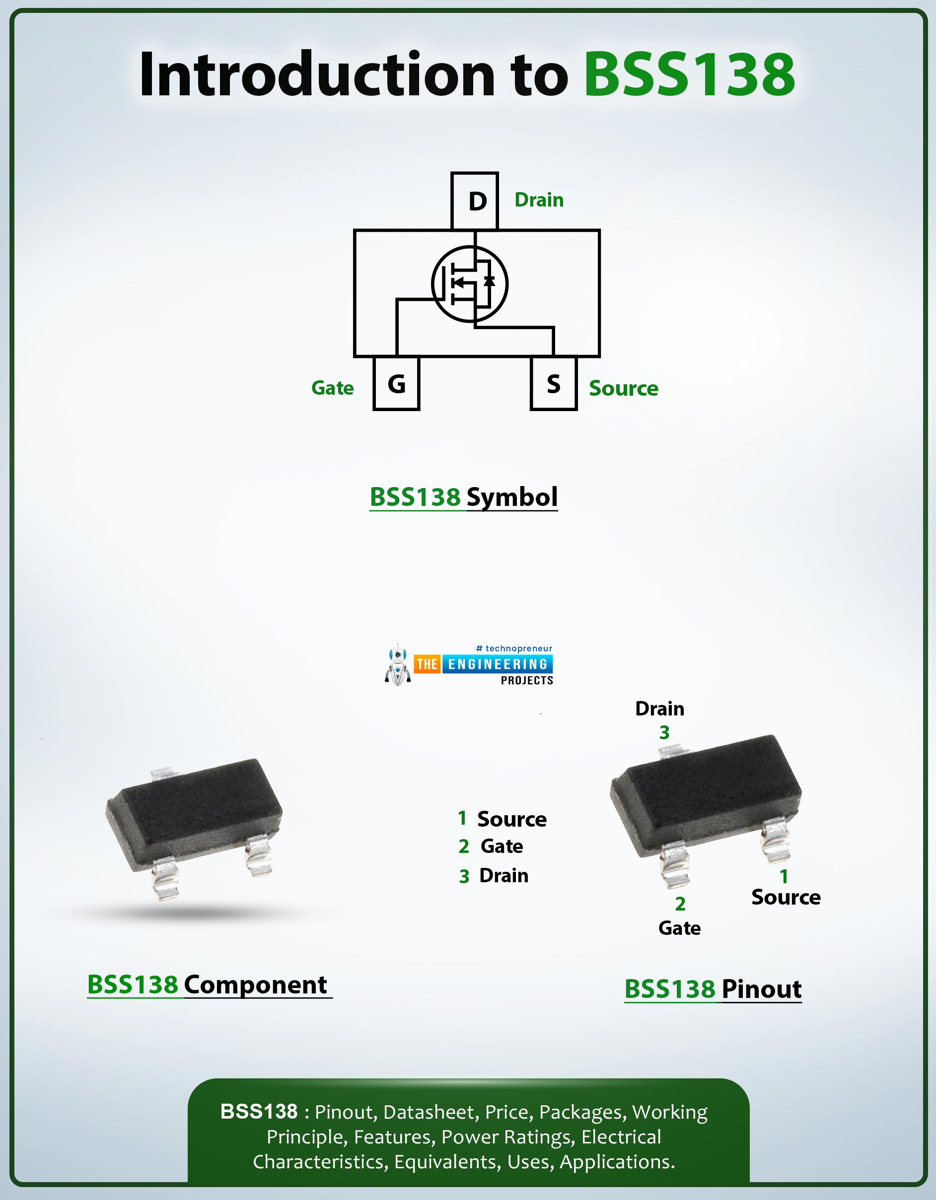
Hi Everyone! Hope you’re well today. I welcome you on board. In this post today, I’ll detail the Introduction to BSS138.

The BSS138 is an N-Channel Logic Level Enhancement Mode Field Effect Transistor that is available in surface mount package SOT-23. It features a low input capacitance of around 40pF and a low on-state resistance of around 3.5. High switching speed and low threshold voltage make this device an ideal pick for level shifter circuit applications.

I suggest you read this post all the way through as I’ll walk you through the complete Introduction to BSS138 covering datasheet, pinout, features, and applications. Let’s jump right in.

Introduction to BSS138

  • The BSS138 is an N-Channel MOSFET mainly used in low current and low voltage switching applications.
  • It contains three terminals called, drain, source, and gate. At times the body is also included in the terminals, making it a four-terminal device.

  • It is important to note that the gate terminal is electrically insulated and contains no current and is normally called an Insulated Gate FET (IG-FET).
  • MOSFETs are categorized into two main types i.e. N-channel MOSFET and P-channel MOSFET. This chip BS138 falls under the category of N-channel MOSFET where electrons are major carriers. While holes are major carriers in P-channel MOSFETs.
  • The electron movement is better than the hole movement. The reason, N-channel MOSFETs are preferred over P-channel MOSFETs for a range of applications.
  • During working with high loads the P-channel MOSFETs turn hot while the N-channel MOSFETs remain cool.
  • BSS138 comes in a continuous drain current of around 200mA and drain-source VDS voltage is 50V.
  • The on-state resistance of this chip is 3.5, while the turn-off and turn-ON time is 20ns each.
  • The compact and robust nature of this device makes it an ideal choice for portable applications including power management circuits and cell phones.
  • The BSS138 is costly compared to its alternative 2n7002. Picking the alternative, you have to compromise with the threshold voltage and on-state resistance.

BSS138 Datasheet

Before you incorporate this component into your electrical project, it’s better to scan through the datasheet of the component that highlights the main characteristics of the device. You can download the datasheet of BS138 by clicking the link below.

BSS138 Pinout

The following figure shows the pinout diagram of BSS138. This device contains three terminals called source, drain, and gate.
Pin Description of BSS138
Pin No. Pin Description Pin Name
1 Electrons enter the channel through the source terminal Source (S)
2 Controls the biasing of the component Gate (G)
3 Electrons leave the channel through the drain terminal Drain (D)

BSS138 Features

The following are the main features of BSS138.
  • Logic Level N-Channel MOSFET
  • Turn ON and Turn OFF time = 20ns each
  • Continuous Drain Current (ID) = 200mA
  • Comes in low on-state resistance
  • Gate threshold voltage (VGS-th) = 0.5V
  • On-state Resistance = 3.5?
  • Drain Source Voltage (VDS) = 50V
  • Gate threshold voltage (VGS-th) = 1.5V
  • Available Package = SOT23 SMD

BSS138 Alternatives

The following are the alternatives to BSS138.
  • IRF540N
  • IRF3205
  • IRF1010E
  • 2N7000
  • BS170N
Before you incorporate these alternatives, double-check the pinout of these equivalents as the pinout of the alternatives might differ from the pinout of BSS138.

BSS138 Applications

This chip is used in the following applications. Used in automotive electronics.
  • Employed as switching devices in electronic control units.
  • Incorporated in low voltage low current applications.
  • Used in automotive electronics.
  • Used as power converters in modern electric vehicles.
  • Used in servo motor control.

That’s all for today. Hope you’ve got a brief insight into the Introduction to BSS138. If you have any questions, you can approach me in the section below, I’d love to help you the best way I can. You’re most welcome to share your valuable feedback and suggestions around the content we share so we keep sharing quality content customized to your exact needs and requirements. Thank you for reading the post.

74LS76 Dual JK Flip-Flop Datasheet, Pinout, Features & Applications

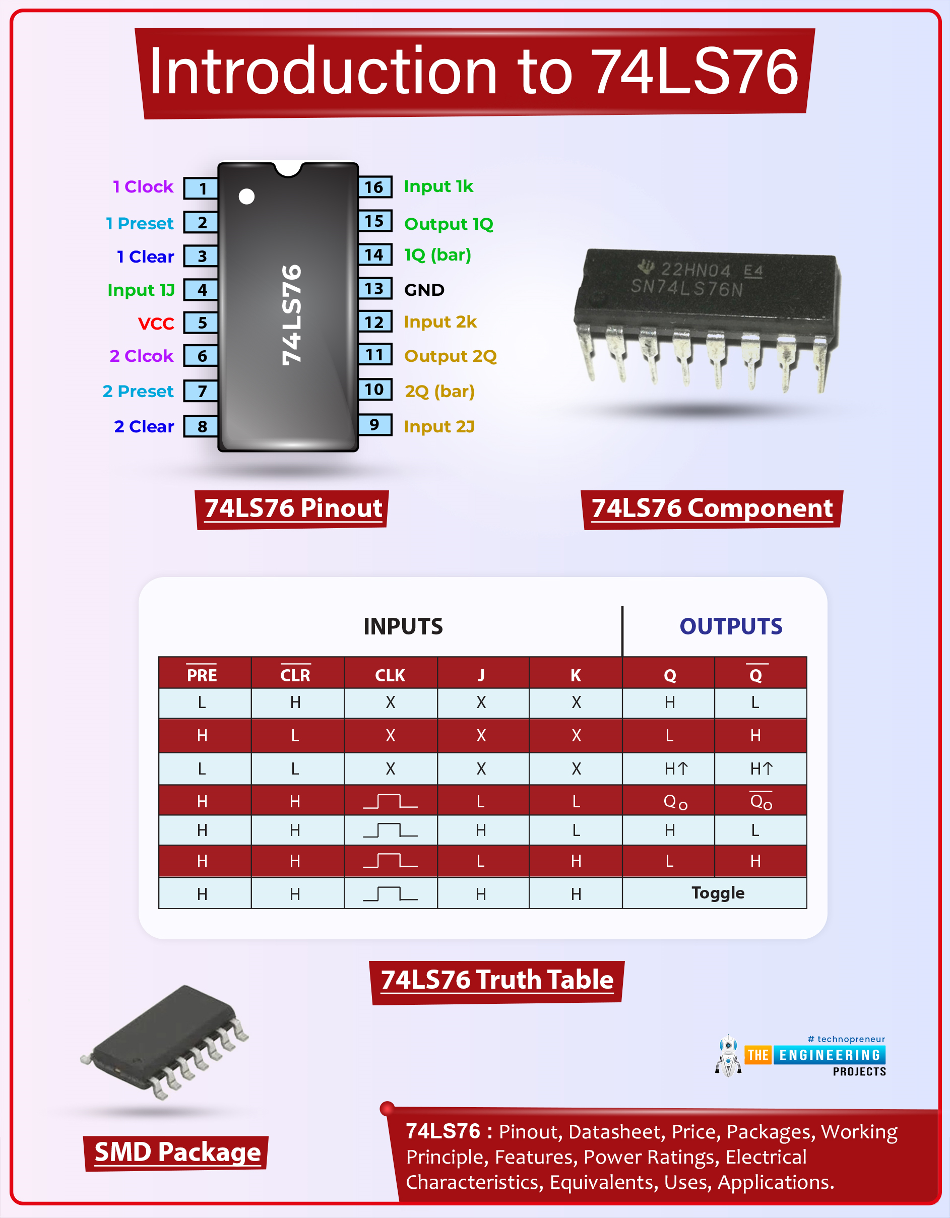
Hi Folks! Hope you’re well today. Happy to see you around. Today, I’ll walk you through the Introduction to 74LS76.

The 74LS76 comes with separate J, K, clock pulse, direct clear inputs, and direct set. These flip-flops are developed in such a way when the clock is set HIGH, data will be received enabling inputs.

I suggest you buckle up as I’ll detail the complete Introduction to 74LS76 covering datasheet, pinout, features, alternatives, and applications.

Introduction to 74LS76

  • The 74LS76 comes with separate J, K, clock pulse, direct clear inputs, and direct set. These flip-flops are developed in such a way when the clock is set HIGH, data will be received enabling inputs.
  • This IC contains two JK flip-flops and each flip-flop can be utilized individually for the required applications.

  • These flip-flops are mainly employed in control registers, shift registers, and storage registers and are termed as latching devices due to their ability to remember every single bit of data.
  • These devices latch the output based on the stored binary data.
  • It is important to note more than one flip-flop can be combined in series for storing a small amount of data as an EEPROM.
  • The operating voltage range of this dual JK flip-flop is 2V to 6V and comes in 14-pin PDIP, GDIP and PDSO packages.
  • This JK flip-flop is termed the best pick for practical applications as it possesses stable output for all types of inputs.
  • The J and K inputs logic levels will be performed as per the Truth Table as long as minimum set-up times are taken into observation.
  • Know that the Input data is converted to the outputs when the HIGH-to-LOW clock transition occurs.
  • This IC houses two JK flip-flops and is powered by +5V.

74LS76 Datasheet

Before you apply this component to your electrical project, it’s wise to scan through the datasheet of the component that highlights the main characteristics of the chip. Click the link below to download the datasheet of 74LS76

74LS76 Pinout

The following is the pinout diagram of 74LS76. The following table represents the pin description of each pin integrated on the chip.
Pin Description of 74LS76 Dual JK Flip-Flop
Pin No. Pin Description Pin Name
1,6 These pins should be provided with a clock pulse for the flip flop Clock-1/ Clock-2
2,7 Preset input pins drive Flip Flop to a set state. Preset-1 / Preset-2
16,12 Input pin of the Flip Flop 1K/ 2K
4,9 Another Input pin of the Flip Flop 1J / 2J
14,10 The inverted output pin of Flip Flop 1Q(bar) / 2Q (bar)
15,11 Output Pin of the Flip Flop 1Q / 2Q
3,8 Clear input pin drives Flip Flop to a reset state. 1 CLR (bar)/ 2 CLR (bar)
13 Connected to the ground Ground
5 Powers the IC with 5V Power (+Vs)

74LS76 Truth Table

The clear and preset are termed as the asynchronous active-low inputs. When they are set LOW, they result in overriding the J-K and clock inputs allow the output to remain in the steady-state levels. The truth table of 74LS76 is shown below.

74LS76 Features

The main features of the chip are described below.
  • Operating Voltage Range = 2V to 6V
  • Low-Level Output Voltage Max. = 0.25V
  • High-Level Output Voltage Min. = 3.5 V
  • Dual JK Flip Flop Chip
  • Operating Temperature Range = -55 to -125°C
  • Low-Level Input Voltage Max. = 0.8 V
  • High-Level Input Voltage Min. = 2 V
  • Available Packages = 14-pin PDIP, GDIP, PDSO

74LS76 Applications

The following are the main applications of flip-flop 74LS76.
  • Employed in Memory/Control Registers
  • Used in Shift Registers
  • Used in Latching devices
  • Incorporated in EEPROM circuits

That’s all for today. Hope you’ve got a clear insight into the Introduction to 74LS76. If you have any questions, you can pop your comment in the section below, I’d love to help you the best way I can. Feel free to share your valuable feedback and suggestions around the content we share so we keep producing quality content tailored to your exact needs and requirements. Thank you for reading the article.

CD4011 NAND Gate Datasheet, Pinout, Features & Applications

Hi Guys! Hope you’re well today. I welcome you on board. In this post today, I’ll detail the Introduction to CD4035.

CD4011 IC belongs to the CD40xx CMOS IC series. The CD4011 chip comes with four independent NAND gates. This device is used to perform the Boolean function Y = A × B or Y = A + B in positive logic. This IC is widely used in many applications including Portable Audio Docks, AV Receivers, and Blu-Ray Players.

I suggest you read this entire post till the end as I’ll walk you through the complete introduction to CD4011 covering datasheet, pinout, features, truth table, alternatives, and applications. Let’s jump right in.

Introduction to CD4011

  • CD4011 IC belongs to the CD40xx CMOS IC series. The CD4011 chip comes with four independent NAND gates.
  • It is important to note that the output voltage and the operating voltage of this IC are equal.

  • This chip is widely used in many electrical circuits including mp3 players, AV receivers, Blu-ray players, and home theater.
  • If you want to use this chip as a logic inverter, you can reconfigure the NAND gates into NOT gates.
  • Less transition time makes this device the best pick for high-speed applications.
  • The typical operating voltage of this device is 5V which comes in 14-pin PDIP, GDIP and PDSO packages.
  • The operating voltage range is -55 to 125C and the propagation delay time is 60ns.

CD4011 Datasheet

Before you incorporate this component into your electrical project, it’s better to scan through the datasheet of the component that comes with the main characteristics of the device. You can download the datasheet of CD4011 by clicking the link below.

CD4011 Pinout

The following figure shows the pinout diagram of CD4011. The following table represents the pin description of each pin available on the chip.
Pin Description of CD4011
Pin No. Pin Description Pin Name
1,2,5,6,8,9,12,13 First Input pin of the NAND gate NAND Gate Input pins
3,4,10,11 The Inverting input pin of the Op-Amp A NAND Gate Output pins
14 5V is used to power the IC Vcc (Vdd)
4 Connect to the ground Ground Vss

CD4011 Features

The following are the main features of CD4011.
  • Typical Operating Voltage = 5V
  • Operating Temperature Range = - 55 C to + 125 C
  • Low-Level Output Current = 1.5mA
  • High-Level Output Current = - 1.5 mA
  • Propagation Delay Time = 60 ns
  • Dual Input NAND Gate – Quad Package
  • Available Packages = 14-pin PDIP, GDIP, PDSO

CD4011 Truth Table

The following figure shows the truth table of CD4011. You can see from the truth table that the output of the device will only be LOW when both inputs of the device are HIGH, in other cases, it will be HIGH.

CD4011 Circuit Diagram

The CD4011 circuit diagram is shown in the figure below. You can see from the image above that this IC comes with four independent NAND gates. It carries 12 input-output pins available for four NAND gates. Power up the IC with VCC and Ground pins. The operating voltage of this device is 5V but it can also work at 7V.

CD4011 Equivalents

The following are the alternative to CD4011.
  • SN54LS00
  • SN74HC00
Before incorporating these alternatives into your project, double-check the pinout of the alternatives as the pinout of the CD4011 might differ from the pinout of the equivalents.

CD4011 Applications

The CD4011 chip is used in the following applications.
  • Employed in portable Audio Docks
  • Used in AV Receivers
  • Used in MP3 Players or Recorders
  • Applied in Home Theater
  • Incorporated in Blu-Ray Players
  • Employed in Personal Digital Assistants (PDAs)

That’s all for today. Hope you’ve got a brief insight into the Introduction to CD4011. If you have any questions, you can pop your comment in the section below. I’d love to help you the best way I can. You’re most welcome to share your feedback around the content we share so we keep sharing quality content tailored to your exact needs and requirements. Thank you for reading the post.

BSS123 N-Channel MOSFET Datasheet, Pinout, Features & Applications

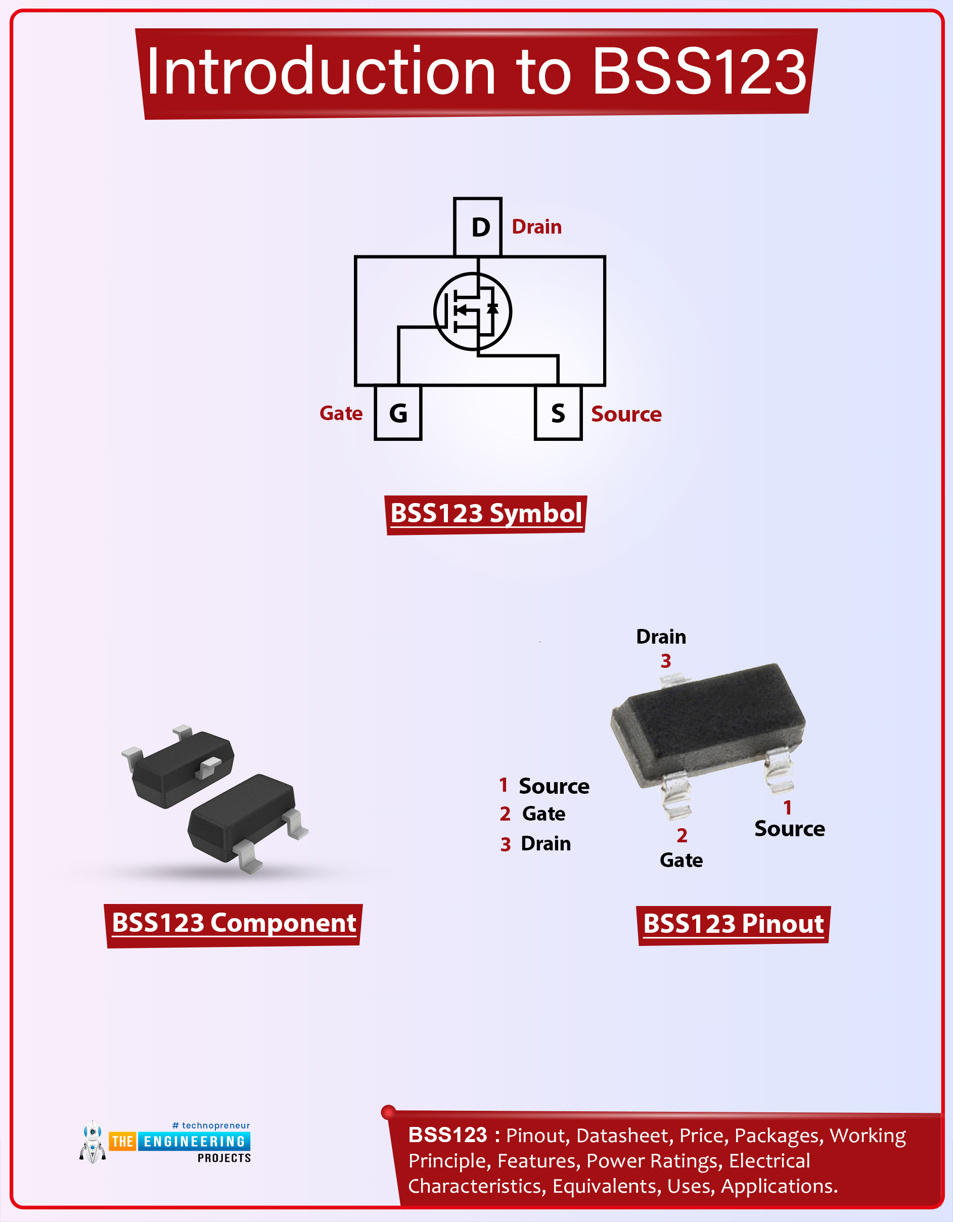
Hi Guys! Hope you’re well today. Happy to see you around. In this post today, I’ll walk you through the Introduction to BSS123.

The BSS123 is an N-Channel Logic Level Enhancement Mode Field Effect Transistor that comes in surface mount package SOT-23. It is a rugged and reliable device that comes with a drain-source voltage of around 100V while the gate-source voltage is -+20V. It is mainly used in low voltage and low current applications like servo motor control and switching and amplification applications.

I suggest you buckle up as I’ll detail the complete Introduction to BSS123 covering datasheet, pinout, features, and applications. Let’s get started.

Introduction to BSS123

  • The BSS123 is an N-Channel Logic Level Enhancement Mode Field Effect Transistor that comes in surface mount package SOT-23.
  • This field-effect transistor is widely used in amplification and switching applications in a range of electronic devices.
  • This is a three-terminal device with terminals named: gate, source, and drain. Sometimes, the body part is also considered as terminal, making it a four-terminal device.

  • The drain current of this component is 170mA and it comes with a low threshold voltage of 1.7V.
  • Know that the gate terminal is electrically insulated since it carries no current and is commonly called as Insulated Gate FET (IG-FET).
  • There are two types of MOSFET i.e. N-channel MOSFET and P-channel MOSFET. This BSS123 chip falls under the category of N-channel MOSFET where electrons are the major charge carriers. In P-channel MOSFETs, holes are the major carrier.
  • The movement of electrons is better than the movement of holes, so N-channel MOSFETs are better than P-channel MOSFETs and possess less resistance. The reason… with high loads the N-channel MOSFETs remain cool while P-channel MOSFET goes hot in the presence of high loads.
  • The charge carriers (electrons in this case of N-channel MOSFET) enter the channel through the source terminal and leave the channel through the drain terminal.
  • The gate terminal stands between the source and drain terminal and the voltage on the gate terminal controls the width of the channel.
  • This N-channel MOSFET is commonly termed a transistor and is used in both digital and analog circuits.
  • The operating temperature and storage junction temperature range of this device is -55C to 150C.
  • The low on-state resistance makes this device the best pick for switching applications.
  • The one drawback of this MOSFET is its low drain current. It offers a peak current of up to 1A at the maximum threshold voltage and a continuous current of 170mA.
  • If you apply ratings more than the required absolute maximum ratings, it will damage the device.

BSS123 Datasheet

While working with this component in your electrical project, it’s wise to go through the datasheet of the component that features the main characteristics of the device. Click the link below to download the datasheet of BSS123.

BSS123 Pinout

The following figure represents the pinout diagram of BSS123. This MOSFET carries three terminals gate, source, and drain.
Pin Description of BSS123
Pin No. Pin Description Pin Name
1 Electrons enter the channel through Source Source (S)
2 Controls the biasing of the MOSFET Gate (G)
3 Electrons leave the channel through Drain Drain (D)

BSS123 Features

The following are the main features of BSS123.
  • The resistance between drain and source terminal RDS (on-state resistance) is 6? at gate-source voltage VGS of 10V and it’s 10? at VGS of 4.5V.
  • High-density cell design leads to extremely low on-state resistance RDS (ON).
  • Drain Source Voltage (VDS) is 100V
  • This chip is rugged and reliable.
  • Comes in a compact industry-standard SOT-23 surface-mount package.
  • The gate threshold voltage (VGS-th) is 1.7V typically
  • Continuous Drain Current (ID) is 170mA
  • Turn ON and Turn off delay time is 1.7ns and 17ns respectively

BSS123 Applications

This MOSFET device is used in the following applications.
  • Used in automotive electronics.
  • Incorporated in low voltage low current applications.
  • Used in servo motor control.
  • Employed as switching devices in electronic control units.
  • Used as power converters in modern electric vehicles.

That’s all for today. Hope you find this article helpful. If you have any questions, you can pop your comment in the section below, I’d love to help you the best way I can. Feel free to share your valuable feedback and suggestions around the content we share so we keep coming back with quality content tailored to your exact needs and requirements. Thank you for reading the article.

74LS74 Dual D Flip-Flop Datasheet, Pinout, Features & Applications

Hi Friends! Hope you’re well today. I welcome you on board. In this post today, I’ll describe the Introduction to 74LS74. 74LS74A flip-flop IC carries the Schottky TTL circuitry to generate high-speed D-type flip-flops. Every flip-flop in this chip comes with individual inputs, and also complementary Q and Q`(bar) outputs. Flip-Flops are normally considered as the basic building blocks of modern digital electronics. These flip-flops are used to store the binary data where stored data can be varied by applying the different inputs. I suggest you buckle up as in this post I’ll walk you through the complete introduction to 74LS74 covering datasheet, pinout, features, and applications. Let’s get started.

Introduction to 74LS74

  • 74LS74A flip-flop IC carries the Schottky TTL circuitry to generate high-speed D-type flip-flops. Every flip-flop in this chip comes with individual inputs, and also complementary Q and Q`(bar) outputs.
  • A flip-flop is a circuit that comes with two stable states and is mainly employed to store binary data.
  • These flip-flops are widely used in communication systems and computers.
  • The working of 74LS74 is simple and straight forward. In order to activate the chip, power the GND and Vcc pin of the chip. In this dual D flip-flop, each flip-flop works independently.
  • To achieve the output at pins 5 and 6, you’ll need to use 1st flip-flip by connecting the input signals 2 and 3. The clock source is produced using MCU or 555 timers and is provided to pin 3. When you keep pin 3 HIGH, it will reset the flip-flop and clear the data.

74LS74 Flip-Flop Table

You can get a hold of the working of this chip by observing the table below where X represents ‘don’t care’

74LS74 Datasheet

Before you incorporate this device into your electrical project, it’s wise to go through the datasheet of the component that features the main characteristics of the component. You can download the datasheet of 74LS74 by clicking the link below.

74LS74 Pinout

The following figure represents the pinout diagram of 74LS74. The following table shows the pin description of each pin incorporated on the chip.
Pin Description of 74LS74
Pin No. & Name Description Symbol
5,9 Output Output Pin of the Flip Flop 1Q / 2Q
6,8 Complementary Output The inverted output pin of Flip Flop 1Q’(bar) / 2Q’(bar)
3,11 Clock Input Pin These pins should be provided with a clock pulse for the flip flop 1CLK / 2CLK
1,13 Clear data Resets the flip flop by clearing its memory 1CLR (bar) / 2CLR (bar)
2,12 Data input pin Input pin of the Flip Flop 1D /2D
4,10 PRE Input Another Input pin for Flip Flop. Also referred to as a set pin 1PRE (bar) / 2PRE (bar)
7 Ground Connected to the ground Vss
14 Supply Voltage Power Supply Vdd/Vcc

74LS74 Features

The following are the main features of 74LS74.
  • Low-Level Input Voltage maximum = 0.8V
  • Operating Voltage range = 2V to 15V
  • Operating Temperature range = 0 to 70°C
  • Dual D Flip Flop Package IC
  • High-Level Output Current = 8mA
  • High-Level Input Voltage minimum = 2 V
  • Propagation Delay = 40nS
  • Available packages = 14-pin SO-14, SOT42

74LS74 Equivalents

The equivalents to 74LS74 are:
  • HEF40312B
  • 74LVC2G80
74LS74 Applications
  • Buffer Circuits
  • Latching devices
  • Used as Shift Registers
  • Sampling Circuits
  • Memory/Control Registers
That’s all for today. Hope you find this article helpful. If you’re unsure or have any questions, you can approach me in the section below, I’d love to help you the best way I can. You are most welcome to share your valuable feedback and suggestions around the content we share so we keep coming back with quality content customized to your exact needs and requirements. Thank you for reading the post.

CD4035 Shift Register Datasheet, Pinout, Features & Applications

Hello Everyone! Hope you’re well today. Happy to see you around. In this post today, I’ll walk you through the Introduction to CD4035.

The CD4035 is a shift register that is mainly used in counters, control circuits, and registers. It contains clocked signal serial chip that is a four-stage register. Synchronous Parallel inputs are provided to each stage and serial inputs are offered to the first stage via JK logic.

I suggest you read this post all the way through as I’ll detail the complete introduction to CD4035 covering datasheet, pinout, features, alternatives, and applications. Let’s jump right in.

Introduction to CD4035

  • The CD4035 is a shift register that is a 16-pin device and is mainly used in control circuits, counters, and registers.
  •  It is a four-stage register that comes with synchronous parallel inputs provided to each stage and is available in 16-pin PDIP, GDIP, and PDSO packages.

  • The CD4035 chip contains two 4-bit Parallel-In & Parallel-Out Shift Registers which project that it is used to receive (input) data parallel and can control 4 output pins in parallel.
  • Simply put, it extracts data from four parallel inputs, and as a result, shifts them and then offers that data on four parallel outputs.
  • It carries the clock input edge that is used for data shifting where data is shifted on every positive clock edge.
  • This four-stage register stage comes with D Flip Flops in each stage that are connected with each other.
  • This chip seems to be the right fit for the applications where microcontrollers don’t have enough GPIO pins to handle the number of outputs.
  • Since this chip can operate as the data bit for LCD, CD4035 can be employed for interfacing LCD screens
  • The frequency of this chip is 12MHz at Vdd = 10V and the propagation delay time is 500ns.
  • While the operating voltage range is 3V to 18V and the operating temperature range is -55C to 125C.

CD4035 Datasheet

Before you integrate this component into your electrical project, it’s wise to go through the datasheet of the component that details the main characteristics of the device. Click the link below and download the datasheet of CD4035.

CD4035 Pinout

The following figure shows the pinout diagram of CD4035. The following table shows the pin number, name, and description of each pin incorporated on the chip.
Pin Description of CD4035
Pin No. Pin Description Pin Name
2 True/Complement Control pin which displays the complement of the data on the output when this pin is LOW T/C (True/Complement)
3,4 Serial Inputs J, ~k
5 This pin is used to reset the output values to 0. R (Reset)
6 Clock input puls C (Clock)
7 Parallel or serial control P/S (Parallel/Serial Control)
8 Ground Pin Vss
9,10,11,12 Parallel data inputs Inputs PI-1 to PI-4
1,13,14,15 Outputs Q0, Q1, Q2, Q3
16 Positive supply terminal Vdd

CD4035 Features

The following are the main features of a CD4035 shift register.
  • Operating Voltage range = 3V to 18V
  • Operating Temperature Range = - 55 C to + 125 C
  • Chip is a Dual 4-bit,  Parallel In – Parallel out Shift register
  • Propagation Delay Time = 500 ns
  • Frequency = 12 MHz (Typ.) at VDD = 10 V
  • Available packages = 16-pin PDIP, GDIP, PDSO

CD4035 Alternatives

The following are the alternatives of CD4035.
  • 4014
  • 74LS379
  • 74LS323
  • 74LS166
  • 74HC595
  • 74LS164
  • 74LS299
Before working with the alternatives, double-check the pinout of the alternatives, as the pinout of equivalents might differ from the pinout of CD4035.

CD4035 Applications

The following are the main applications of this four-stage shift register.
  • Shift-left — shift right registers
  • Counters, Registers
  • Sequence generation
  • Code conversion
  • Serial-to-parallel/parallel-to-serial conversions
  • Arithmetic-unit registers
  • Control circuits

That was all about the Introduction to CD4035. If you’re unsure or have any questions, you can approach me in the section below. I’d love to help you the best way I can. Feel free to share your feedback around the content we share so we keep coming back with quality content customized to your exact needs and requirements. Thank you for reading the post.

Syed Zain Nasir

I am Syed Zain Nasir, the founder of <a href=https://www.TheEngineeringProjects.com/>The Engineering Projects</a> (TEP). I am a programmer since 2009 before that I just search things, make small projects and now I am sharing my knowledge through this platform.I also work as a freelancer and did many projects related to programming and electrical circuitry. <a href=https://plus.google.com/+SyedZainNasir/>My Google Profile+</a>

Share
Published by
Syed Zain Nasir