Police Siren Project using 555 Timer in Proteus

Hey Geeks! Welcome to The Engineering Projects. We hope you are having a reproductive day. We know that sirens are the special sounds that are the symbol that something unusual is occurring or about to occur. You may have experienced the Siren of the Walkthrough Gates at the airport when a person having the knife or other forbidden material pass through it. Or you have heard the Siren of the ambulance and seen that all the traffic gives the way to the ambulance when they hear the special Siren of the Ambulance. The same is the case with the police Siren. The Police sirens are the special sound and it is set with the help of 555 Timer Integrated Circuit. You will learn how can one design a Police siren using the 555 Timer circuit in this tutorial. Let's have a quick list of the topics that will be clear in our tutorial.
  1. What is the 555 Timer Police Siren?
  2. What are the 555 Timer and its modes?
  3. How does the circuit of 555 Timer police Timer Circuit works?
  4. How can you design the circuit of 555 Timer Police Siren in Proteus?
Where To Buy?
No.ComponentsDistributorLink To Buy
1555 TimerAmazonBuy Now
2LEDsAmazonBuy Now
3ResistorAmazonBuy Now

555 Timer Police Siren

The Police Siren we have seen many times in real life as well as in Television shows and Movies are made of the special arrangement of the 555 Timer. The Siren has a loud voice that can be heard at a distance of many feet. This Project has a very simple yet amazing arrangement of some basic electronic devices. The heart of Police Siren is the 555 Timer integrated circuit. In the police siren, two 555 timers are used. This is a Multi-functional chip that is widely used in different types of the industrial as well as household applications. If we look at the configuration of 555 Timer Integrated Circuit then we can generate a table just as shown next:
Pin Number Attachments
1 Ground
2 Trigger
3 Output
4 Reset
5 Control
6 Threshold
7 Discharge
8 Vcc
Technically, The 555 Timer works in 3 modes:
  • Monostable Mode
  • Astable Mode
  • Multistable Mode

Monostable Multivibrator Mode in 555 Timer

This mode of the 555 Timer contains a single stable state that can be used to get only one single output pulse of a specific width that may be high or low by applying an external trigger pulse. In this circuit, the 555 Timer uses only one resistor but two capacitors.

Astable Mode in 555 Timer

As the name shows, the Astable mode does not have any stable state. The Astable mode of 555 Timer has 2 quasi-steady states that change from one state to another one after the other. In this way, the 555 Timer in this state, alters the output from high to low and vise versa after the time settled by the user. It uses two capacitors and two resistors connected with the specific pins in a specific manner.

Bistable Mode of 555 Timer

In this mode of 555 Timer, the pins are connected with two resistors, one capacitor and two switches. The switches turn the state of 555 Timer to high and low and thus we obtained the high and low output waves at a time.

Working of the 555 Timer Police Siren

The working of the 555 Timer Police Siren starts from the Direct Current power supply that is supplied to pins 8 of the 555 Timer.
  1. Both of these 555 Timers are in the Astable mode that means their pulse output changes continuously.
  2. The 555 Timer at the left produces a pulse that is fed into the right 555 Timer as an input.
  3. The values of Resistors control the width of the pulses.
  4. The capacitors connected with the 555 Timers charge and discharge without any interval.
  5.  At the end, this DC power supply enters the speaker with a continuously varying pulses of the current and produces a special sound.
  6. If you want to change the output voice, you can change the values of Resistors and capacitors.

Circuit design of 555 Timer Police Siren in Proteus

To design this circuit, simply follow these step given next as it is.
  • Start the Proteus Software.
  • Choose the required devices from the pick library by clicking the "P" button and writing the names of the devices.

Required Components fpr 555 Timer Police Siren:

  1. NE555 Timer (We'll use 2 ICs)
  2. Diode
  3. Resistor
  4. Direct current power supply
  5. Speaker
  6. Capacitor
  • Get the 555 Timer from the library and arrange it at the working area.
  • Repeat the step above.
  • Choose Resistor, capacitor, Diode and speaker and arrange them on the screen.
  • Change the alignment of 4 resistors and diode by left click on screen> Rotate Clockwise and set the whole circuit as shown in the figure:
  • Go to Generation Mode>DC and fix it at above the working area.

DID YOU KNOW ???

"If you have the Proteus 8 software, then you can have a real time Siren sound by choosing the Speaker and a piano symbol with it."
  • Label the Components by double-clicking it because Proteus throws an error for the duplicate devices.
  • Double click the components mentioned below and change their values according to the table given next:
Device Value
R2 68k Ohm
R3 68K Ohm
R4 8.2K Ohm
R5 8.2K Ohm
C1 100uF
C2 100nF
C3 0.01uF
C4 10uF
Vcc 4V
 
    • Go to Terminal Mode>Ground and Set the Ground terminal just below the circuit.
  •  Join the 555 Timer's pins with the components as described above in the 555 Timer section.
  • Pop the Play button and simulate the circuit.

Task

Now, change the values of capacitor and resistor in different sequence to have the different voices as an output.
Have you heard the siren? If yes then cool. Yet, if no, then look at the circuit deeply and fix the mistake. Truss, today we saw that what is the Police Siren, how does the 555 Timer circuit works, what is the working mechanism of the 555 Timer Police Siren, how does we design the circuit of 555 Timer Police Siren in the Proteus. If you found it useful, give us feedback. If you faced any difficulty, share with us i the comment section. Stay with us with more Proteus Projects.

Download Proteus Library of Arduino Modules

Hi Friends! Glad to have you on board. In this post today, we’ll cover How to Download Proteus Library of Arduino Modules.

If you are a regular reader of our blog, you must have noticed that we are sharing Proteus Libraries of different embedded sensors & modules on regular basis. Moreover, we have also launched version 2.0 of few libraries. So, today I am going to provide links to download Proteus Library of all Arduino Boards designed by TEP.

So, let's get started with How to Download Proteus Library of Arduino Modules:

Where To Buy?
No.ComponentsDistributorLink To Buy
1Arduino Mega 2560AmazonBuy Now
2Arduino NanoAmazonBuy Now
3Arduino UnoAmazonBuy Now

Download Proteus Library of Arduino Modules V2.0

  • It's the most advanced version of Arduino Proteus Library and consists of 6 Arduino Boards in total, named as:
    • Arduino UNO
    • Arduino Mega 2560
    • Arduino Mega 1280
    • Arduino Pro Mini
    • Arduino Nano
    • Arduino Mini
  • We have designed 7 Arduino Proteus Libraries V2.0 in total.
  • First, we have designed seperate Proteus Libraries of these 6 boards while in the 7th Library, we have combined all these boards.
  • So, if you just want to use Arduino UNO, then download its respective Library but if you are working on multiple boards, then download the combined version(7th).
Let's have a look at these Arduino Proteus Libraies one by one:

1. Arduino Uno Library for Proteus V2.0

This Arduino Proteus Library contains only one board named Arduino UNO. You need to download zip file of Proteus library and will be able to simulate Arduino Uno in Proteus software. Proteus Library zip file download link is given below: Download Arduino UNO Library for Proteus V2.0

2. Arduino Mega 2560 Library for Proteus V2.0

Using this Proteus Library, you can simulate Arduino Mega 2560 in Proteus ISIS. Here's the link to download its zip file: Download Arduino Mega 2560 Library for Proteus V2.0

3. Arduino Mega 1280 Library for Proteus V2

Here's the link to dowload Proteus Library zip file of Arduino Mega 1280: Download Arduino Mega 1280 Library for Proteus V2.0

4. Arduino Mini Library for Proteus V2

Here's the link to download Arduino Mini Library for Proteus V2.0: Download Mini Library for Proteus V2.0

5. Arduino Nano Library for Proteus V2.0

Download this Arduino Nano Library for Proteus(V2.0) and simulate it in Proteus ISIS. Here's the Proteus Library zip file download link: Download Arduino Nano Library for Proteus V2.0

6. Arduino Pro Mini Library for Proteus V2.0

Check out this Arduino Pro Mini Library for Proteus(V2). It is similar to the V1 Arduino Pro Mini board but comes in a smaller size. Download Arduino Nano Library for Proteus V2.0

7. Arduino Library for Proteus V2.0

Arduino Library for Proteus contains all 6 Arduino boards. Simply sownload its zip file and you can use any of these 6 Arduino boards. Here's the link to download zip file of Arduino Proteus Library: Download Arduino Library for Proteus V2.0

Arduino Library for Proteus V1.0

In this section, we’ll cover Arduino Library for Proteus V1.0. We’ve designed this library for six different types of Arduino boards.

1. Arduino Mega 2560 Library for Proteus V1

Check out this Arduino Mega 2560 Library for Proteus(V1). Using this library you can simulate Arduino Mega 2560 in the Proteus workspace.
  • Arduino Mega 2560 is a powerful and application-type Arduino board, based on the Atmega2560 microcontroller.
  • It comes with 16 analog pins and 54 digital I/O pins, including 15 pins for PWM.

2. Arduino Mega 1280 Library for Proteus V1

Read this Arduino Mega 1280 Library for Proteus(V1). In this library, we’ve discussed how to download the Arduino Mega 1280 library and use it in your Proteus software. Arduino Mega 1280 is a compact and efficient Arduino board based on the Atmega1280 microcontroller. There are 16 analog and 54 digital I/O pins incorporated on the board. Moreover, it includes a power jack, reset button, ICSP header, and 4 UART serial ports.

3. Arduino Mini Library for Proteus V1

Download Arduino Mini Library for Proteus(V1). You’ll get to know how to simulate Arduino Mini in Proteus. Arduino Mini is a small-sized, robust, and powerful Arduino board, based on an Atmega328 microcontroller. It comes with 14 digital I/O pins, of which 6 pins are used for PWM.

4. Arduino Nano Library for Proteus V1

Click this Arduino Nano Library for Proteus(V1) and simulate Arduino Nano in Proteus software. Arduino Nano is a small, flexible, and breadboard-friendly Arduino board, based on ATmega328p/Atmega168 microcontroller. It features 8 analog pins, 14 digital I/O pins, 2 reset pins & 6 power pins.

5. Arduino Pro Mini Library for Proteus V1

Check out this Arduino Pro Mini Library for Proteus(V1). Arduino Pro Mini is a compact, small-sized Arduino board, based on the Atmega328 microcontroller. It features 8 analog pins, 14 digital I/O pins, of which 6 pins are used as PWM.

6. Arduino Uno Library for Proteus V1

Download Arduino Uno Library for Proteus(V1) and simulate Arduino Uno in Proteus software. Arduino Uno is a unique, application-type Arduino board, based on the Atmega328 microcontroller.

7. Arduino Library for Proteus V1.0

  That’s all for today. Approach me in the section below if you need any help, I’d love to assist you the best way I can. Thank you for reading this post.

What is IGBT? Full Form, Pinout, Meaning, Symbol & Working

Hi Guys! Hope you’re well. In this post today, we’ll cover What is IGBT? We’ll also discuss IGBT Full Form, Pinout, Meaning, Symbol & Working.

BJT (bipolar junction transistor) and MOSFETs (metal-oxide-semiconductor field-effect transistor) are commonly used electronic switches that we’ve already studied in detail. These devices are useful when you deal with low-current applications, however, when it comes to high-current applications, these devices don’t work as expected. This is where the IGBT transistor comes in handy. This device is a combination of both BJT and MOSFET and stands fit for high-current applications. In this post, we’ll cover What is IGBT in detail. Let’s get started:

1. What is IGBT?

IGBT is a three-pin device made of semiconductor material and is used for fast-switching applications. It comes with input characteristics of the MOSFETs and output characteristics of the BJT.

IGBT Full Form

IGBT stands for Insulated Gate Bipolar Transistor.

IGBT Symbol

The following figure shows the IGBT symbol. You can see from the symbol that IGBT is a combination of both MOSFET and BJT.

IGBT Pinout

The following figure shows the IGBT Pinout.

IGBT Meaning

The Insulated Gate Bipolar Transistor comes with the insulated gate from the MOSFET at the input with the conventional bipolar transistor at the output. The emitter and collector terminals are the conduction pins of the IGBT. While the gate terminal at the input is the control terminal. The conduction is controlled by the gate terminal. The insulated gate bipolar transistor comes with current and voltage ratings similar to that of the bipolar junction transistors… when IGBT is used as a static controlled switch. But what makes IGBT a simpler device compared to BJT is the inclusion of an isolated gate terminal from the MOSFET. The IGBT consumes less power in the presence of an isolated gate terminal.

2. IGBT Working

  • Like MOSFETs, IGBT is a voltage-controlled device which means the only small voltage is required at the gate terminal to initiate the conduction process. IGBT can switch current from collector to emitter terminal which means it can switch in the forward direction only.
  • The following figure shows the IGBT switching circuit. In this case, a small voltage is applied at the gate terminal which results in the switching of the motor from a positive supply. The resistor is included to control the current passing through the motor.
  • The graph below shows the IGBT input characteristics. It is a graph between the voltage applied at the gate terminal vs current passing through the collector terminal.
  • No current will flow through the IGBT when there is no voltage applied at the gate pin. In this case, the transistor will remain turned off. However, when voltage is applied at the gate terminal, the current will remain zero for a little while. When the voltage exceeds the threshold voltage, the device will start conducting and current will flow from collector to emitter terminal.
  • The graph below shows the IGBT output characteristics. This is a graph between the voltage at the collector and emitter terminals vs current passing through the collector terminal.
  • This graph contains three stages. The first one is the cut-off region when there is no voltage applied at the gate terminal. At this stage, the transistor will remain turned off and there will be no current flowing through the transistor.
  • When the voltage at the gate terminal increases, and if it stays below the threshold voltage, it will result in the small leakage current flowing through the device but the device will remain in the cut off region.
  • However, when the applied voltage at the gate terminal exceeds the threshold voltage the device will move to the active region and in this case, a significant current will flow from collector to emitter terminal.
  • At this stage, applied voltage and resulting current will be directly proportional to each other. More voltage will result in more current flow at the collector terminal.

3. IGBT Modules

IGBT is used in a range of electronic switching applications where both BJT and MOSFET fail to deliver the desired results in high current applications. This hybrid combination of two transistors features voltage-controlled characteristics like MOSFETs and conduction and switching characteristics like BJT. The IGBT devices are divided into two main types.
  1. Non-Punch Through IGBT [NPT-IGBT]
  2. Punch Through [PT-IGBT]
Let’s discuss them one by one.

1. Non-Punch Through IGBT [NPT-IGBT]

  • These IGBTs are also called symmetrical devices. The IGBT transistors that come with an n+ buffer layer are called Punch Through-IGBT (PT-IGBT)
  • They are called symmetrical devices because both reverse and forward breakdown voltages are the same in this case. They are more thermally stable and more rugged in short-circuit failure mode.
  • Moreover, the changing temperature won’t have a significant effect on turn-off loss i.e. it remains unchanged with temperature. And the P-layer (collector side) is highly doped in Non-Punch Through IGBT.
  • They are developed with less expensive diffusion process technology, making them ideal choices for AC circuits.  Plus, the structure of NPT ensures the bidirectional blocking capability in these devices. The N base is thick in this case.

2. Punch Through [PT-IGBT]

  • These IGBTs are also called asymmetrical devices. They are called asymmetrical because here forward breakdown voltage is more than the reverse breakdown voltage.
  • These devices are less thermally stable and less rugged in short-circuit failure mode. And in this case, turn-off loss is directly proportional to temperature, it increases significantly with the increase in temperature.
  • These IGBTs are manufactured using an expensive N-epitaxial water process. They contain a thin N base and the PT structure comes with lower reverse blocking capability.
  • They are widely used in DC circuits where the voltage support in the reverse direction is not needed by the device.

4. IGBT vs MOSFET

  • Both IGBT and MOSFETs are transistors and voltage-controlled devices but they are different in terms of composition and performance.
  • IGBT is composed of collector, emitter, and gate pins, whereas MOSFET, on the other hand, is made of the drain, source, and gate terminals. IGBT is better than MOSFETs in terms of performance.
  • IGBT needs an extra freewheeling diode to drive the current in a reverse direction. The inclusion of this freewheeling diode makes this device the best pick for high voltage applications.
  • IGBT is preferred for high voltage (more than 1000V), low frequency (Less than 20 kHz), small or narrow load or line variations; high operating temperature; low duty cycle, and, more than 5kw output power rating applications.
  • MOSFET, on the other hand, is preferred for large duty cycles, wide load or line variations, high frequency (more than 200KHz), and low voltage (Less than 250V) applications.
  • After the MOSFET, the IGBT is widely employed in electronic devices. The IGBT covers 27% of the power transistor market.
  • The greater power gain and lower input losses of IGBT make this device preferable over both MOSFETs and BJT. You’ll find high-voltage and high-current bipolar transistors in the market, but they come with one drawback.
  • Their switching speed is not so good, they take time to switch the devices. Similarly, MOSFETs alone have high switching speeds, no doubt. But high-current and high-voltage MOSFET components are too expensive compared to IGBT.

5. IGBT Inverter

The IGBT transistors are employed in VFD (variable frequency drive) inverter modules as the high power electronic switch due to the following reasons.
  • It carries a high current-carrying capacity. Some IGBT devices come with a maximum rated collector current Ic (max) of around 100A. And if this fails to meet the requirement, two or more IGBTs can be combined to meet the purpose.
  • IGBTs come with the open circuit rated collector voltage up to 1.6kV. This explains there are devices preferable for functions off rectified three and single phase mains… ranging from 110Vac to 690Vac.
  • An IGBT contains a high impedance gate terminal which projects it is technically simple to control the device by controlling the gate terminal.
 
  • The low conduction losses of the IGBT ensure a low on-state voltage.
  • Recall, the IGBT carries a fast switching speed. This means you can achieve high switching frequencies with reduced switching losses that play a key role in motor noise and harmonic reduction.
  • The IGBT carries a wide Reverse Bias Safe Operating Area (RBSOA) that explains it is comparatively secured against load short circuits.
Know that the properties mentioned above may affect each other. An IGBT, for example, often comes with a very fast switching speed that guarantees higher on-state saturation voltage - that is a property of the manufacturing method. So this sets the trade-off between conduction losses and switching losses. This explains that for a large high-power VFD, you may require to pick slower devices with quite low saturation voltage, to minimize the total losses. Moreover, you can reduce switching losses by working with a lower modulation frequency.

6. IGBT Applications

The combination of high switching speed like MOSFETs and low conduction loss like BJT will result in developing the optimal solid-state of IGBT, making it a suitable pick for a range of applications. The following are the IGBT applications.
  • Used in AC and DC motor drives
  • Employed in Unregulated Power Supply (UPS)
  • Used in Switch Mode Power Supplies (SMPS)
  • Used in electric cars and plasma physics
  • Employed in traction motor control and induction heating
  • Incorporated in inverters, converters, and power supplies

That’s all for today. Hope you find this article helpful. If you have any questions, you can pop your comment in the section below. I’m happy and willing to assist you the best way I can. Feel free to share your valuable suggestions and feedback around the content we share so we keep coming back with quality content tailored to your needs and requirements. Thank you for reading the article.

2SC2240 Datasheet, Pinout, Power Ratings, Equivalents & Applications

Hello Everyone! Happy to see you around. In this post today, we’ll cover the 2SC2240 NPN Transistor. We will have a look at the 2SC2240 Datasheet, Pinout, Power Ratings, Equivalents & Applications.

Electrons are the majority charge carriers in this NPN transistor, in contrast to PNP transistors, where holes are the majority carriers. The 2SC2240 comes with a power dissipation of 0.3W, the amount of energy this transistor dissipates while operating in the forward-biased state, while the collector current is 0.1A means it can support load up to 0.1A.

This NPN transistor contains 3 terminals, named:

  1. Emitter
  2. Collector
  3. Base

If the voltage at the base terminal is above 0.7V, the transistor will get forward-biased and the current will start flowing from Collector to Emitter terminal. If the base voltage is less than 0.7V, it will remain reverse-biased.

So, let's have a look at the 2SC2240 NPN Transistor in detail. Let’s get started:

2SC2240 NPN Transistor

  • The 2SC2240 is a bipolar junction transistor that belongs to the NPN transistor family.
  • This component is mainly used for switching and amplification purposes and comes in a TO-92 package.
  • 2SC2240 comes with three layers, with one p-doped layer between two n-doped layers.
  • The two n-doped layers represent the Collector and Emitter, while the p-doped layer represents the Base Terminal.

  • This device contains three terminals: the base, collector, and emitter. The collector terminal collects the electrons coming from the base side and the emitter terminal emits the electrons into the base terminal.
  • The NPN transistors contain two junctions known as collector-base junction and emitter-base junction.
  • The transistor is said to operate in a Forward-Biased state, when the collector-base junction is reverse-biased, while the emitter-base junction is forward-biased.
  • When a negative voltage is applied at the emitter side and a positive voltage is available at the base terminal then we can make the emitter-base junction forward biased.

NPN vs. PNP: A Quick Recall

  • Bipolar Junction Transistors(BJTs) are categorized into two types i.e. NPN transistors and PNP transistors. This is a bipolar transistor, which means both electrons and holes play a role in the conductivity process inside the transistor.
  • But electrons are the major carriers in NPN transistors while in the case of PNP transistors, holes are the major carriers.
  • NPN transistors are preferred over PNP transistors because the mobility of electrons is more efficient than the mobility of holes.
  • These bipolar devices are called current-controlled devices, in opposition to MOSFETs, which are called voltage-controlled devices and carry terminals like a drain, source, and gate.

2SC2240 Datasheet

It’s wise to go through the 2SC2240 datasheet before you apply this device to your electrical project.

2SC2240 Pinout

The following figure shows the 2SC2240 pinout.

This component contains three terminals named: 1: Emitter 2: Collector 3: Base

  • These terminals differ in terms of size and doping concentration and are used for external connection with the electronic circuit. The emitter side is highly doped and the base side is lightly doped and the collector terminal is moderately doped.
  • The collector terminal dissipates more energy compared to the other two terminals. It is bigger in size compared to base and emitter terminals. The large surface area of the collector side guarantees more heat dissipation.

2SC2240 Working Principle

The base is responsible for the transistor action. When voltage is applied at the base terminal, it will bias the device and as a result, the current will flow from collector to emitter terminal. As this is an NPN transistor so here current will flow from the collector to the emitter side and in the case of the PNP transistor current will flow from the emitter to the collector side. These bipolar devices are not symmetrical in nature. This projects if we exchange the emitter and collector pins then these terminals will start working in reverse active mode and will stop working in forward active mode. The different doping concentrations of these pins are the reason this device lack symmetry.

2SC2240 Power Ratings

The following table shows the 2SC2240 power ratings.
Absolute Maximum Ratings of 2SC2240
Pin No. Pin Description Pin Name
1 Collector-emitter voltage 120V
2 Collector-base voltage 120V
3 Base-emitter voltage 5V
4 Collector current 0.1A
5 Power dissipation 0.3W
6 Current gain 200 to 700
7 Operating and storage junction temperature range -55 to 125C
  • If these ratings are applied more than the required time, they can affect the device reliability.
  • The collector-current is 0.1A which defines the amount of load this component can support.
  • The power dissipation is 0.3W which represents the amount of energy released during the working of this component.
  • The current gain ranges from 200 to 700 which is the amount of current this device can amplify.
  • The operating and storage junction temperature ranges from -55 to 125C.
  • The emitter-base voltage is 5V represents the voltage required to bias this component. The collector-base voltage and collector-emitter voltage both are 120V.
  • When using this device, make sure these ratings don’t exceed the absolute maximum ratings else they can damage the device.

2SC2240 Equivalents

The following are the 2SC2240 equivalents.
  • 2SC3201
  • 2SC3245A
  • 2SC3200
  • 2SC3245
  • 2SC2459
  • KTC3200
Before applying alternatives into your projects, double-check the pinout of these equivalents as the pinout of 2SC2240 might differ from the pinout of the alternatives. The 2SA970 is a complementary PNP transistor to the 2SC2240.

2SC2240 Applications

The following are the 2SC2240 applications.
  • Incorporated in modern electronic circuits.
  • Used in Bistable and Astable multivibrators circuit.
  • Used in voltage regulator circuits.
  • Used in a common power amplifier.
  • Used in electronic Ballasts.
  • Used in energy-saving lights.
  • Employed to support loads under 0.1A.
  • Used in the high switching power supply.
  • Used in high-frequency power transform.

2SC2240 Physical Dimensions

The following diagram shows the 2SC2240 physical dimensions.

With physical dimensions, you can evaluate the space required for this device in the electrical project.

That’s all for today. Hope you find this article helpful. Feel free to share your valuable feedback and suggestions around the content we share. They help us produce quality content based on your needs and requirements. If you’re unsure or have any questions, you can approach men in the section below. I’m happy and ready to help you the best way I can. Thank you for reading this post.

KSC1845 Datasheet, Pinout, Power Ratings, Equivalents & Applications

Hi Guys! I welcome you on board. In this post today, we’ll discuss the KSC1845 NPN Transistor. We will have a look at the KSC1845 Datasheet, Pinout, Power Ratings, Equivalents & Applications in detail. As it's an NPN transistor, electrons are the majority charge carriers and thus play a major role in conductivity. KSC1845 is mainly used for fast-switching and amplification purposes.

NPN transistor carries 3 terminals, known as:

  • Emitter
  • Collector
  • Base

If the applied voltage at the base terminal exceeds 0.7V, it will forward bias this NPN transistor and the current will start to flow from Collector to Emitter. If the base voltage is less than 0.7V, KSC1845 will remain in the reverse-biased state.

I suggest you buckle up as I’ll discuss the KSC1845 NPN Transistor in detail. Let’s get started:

KSC1845 NPN Transistor

  • The KSC1845 is a bipolar junction transistor that falls under the NPN transistor family.
  • It is made of silicon semiconductor material and comes in a TO-92 package.
  • The NPN transistors carry two junctions known as emitter-base junction and collector-base junction.
  • When the emitter-base junction is forward-biased and the collector-base junction is reverse-biased, the transistor starts to conduct.
  • KSC1845 Pinout, Symbol and SMD Package are shown in the below figure:

  • We can make the emitter-base junction forward-biased, by applying a negative voltage at its Emitter and a positive voltage at its Base.
  • KSC1845 contains three layers where one p-doped layer sits between two n-doped layers. The p-doped layer represents the base terminal while the other two n-doped layers represent Collector and Emitter.
  • In a forward-biased state, the Emitter emits the electron into the Base while the Collector collects the electrons coming from the Base.

NPN vs PNP

KSC1845 is a Bipolar Junction Transistor, so let's quickly recall it:

  • The bipolar junction transistors come in two types i.e. NPN transistors and PNP transistors. Both holes and electrons play a role in carrying out the conductivity process inside the transistor.
  • In PNP transistors, holes are the majority charge carriers, while in NPN transistors, electrons are the majority charge carriers.
  • Know that the mobility of electrons is better than the mobility of holes, that's why NPN transistors are preferred over PNP transistors for a range of applications.
  • These bipolar(BJT) components are called current-controlled devices in opposition to MOSFETs, which are considered voltage-controlled devices and carry terminals like a drain, source, and gate.

KSC1845 Datasheet

Before you incorporate this device into your electrical project, it’s wise to go through the KSC1845 datasheet that details the main characteristics of the device. Click the link below to download the KSC1845 datasheet.

KSC1845 Pinout

The following figure shows the KSC1845 pinout.

This component contains three terminals named: 1: Emitter 2: Collector 3: Base All these terminals are used for the external connection with the electronic circuit. These terminals differ in terms of size and doping concentration. The base side is lightly doped and the emitter side is highly doped while the collector side is moderately doped. The collector side dissipates more energy because it is bigger in size compared to other terminals. The large surface area of the collector side ensures more heat dissipation.

KSC1845 Working Principle

The base side is the main region that initiates the transistor action. When voltage is applied at the base terminal, it will bias the device and as a result, current starts flowing from collector to emitter side. These bipolar devices are not symmetrical in nature. Which means if we exchange the emitter and collector sides then these terminals will stop working in forward active region and start working in reverse active mode. The different doping concentrations of these terminals ensure the lack of symmetry.

KSC1845 Power Ratings

The following table represents the KSC1845 power ratings.
Absolute Maximum Ratings of KSC1845
Pin No. Pin Description Pin Name
1 Collector-emitter voltage 120V
2 Collector-base voltage 120V
3 Base-emitter voltage 5V
4 Collector current 0.05A
5 Power dissipation 0.5W
6 Current gain 200
7 Operating and storage junction temperature range -55 to 150C
  • When using this device, make sure these ratings don’t exceed the absolute maximum ratings else they can damage the device.
  • Plus, if these ratings are applied more than the required time, they can affect the device reliability.
  • The collector-current is 0.05A which shows the amount of load this device can support.
  • The power dissipation is 0.5W which represents the amount of energy released during the working of this component.
  • The current gain is 200 which shows the amount of current this device can amplify.
  • The collector-base voltage is 120V and the collector-emitter voltage is 120V. The emitter-base voltage is 5V represents the voltage required to bias this component.

KSC1845 Equivalents

The following are the KSC1845 equivalents.
  • FJV1845

Before applying alternatives into your projects, double-check the pinout of these alternatives as the pinout of KSC1845 might differ from the pinout of the equivalents.

The KSA992 is a complementary PNP transistor to the KSC1845.

KSC1845 Applications

The following are the KSC1845 applications.
  • Incorporated in modern electronic circuits.
  • Used in high-frequency power transform.
  • Used in electronic Ballasts.
  • Used in voltage regulator circuits.
  • Used in a common power amplifier.
  • Used in Bistable and Astable multivibrators circuit.
  • Used in energy-saving lights.
  • Employed to support loads under 0.05A.
  • Used in the high switching power supply.

KSC1845 Physical Dimensions

The following diagram shows the KSC1845 physical dimensions.

The KSC1845 physical dimensions help you evaluate the space required for this component in the electrical project.

That’s all for today. Hope you find this article helpful. If you’re unsure or have any questions, you can pop your comment in the section below. I’m ready to help you the best way I can. Feel free to share your valuable feedback and suggestions around the content we share. They help us produce quality content based on your needs and requirements. Thank you for reading the article.

2SC1345 Datasheet, Pinout, Power Ratings, Equivalents & Applications

Hi Guys! Hope you’re well today. In today's tutorial, we will have a look at the 2SC1345 NPN Transistor. We will also discuss 2SC1345 Datasheet, Pinout, Power Ratings, Equivalents & Applications. As this is an NPN transistor, the conductivity is mainly carried out by electrons as the major charge carriers. 2SC1345 is mainly used for switching and amplification purposes.

Let's first recall NPN transistors: NPN transistor comes with 3 terminals, named:

  1. Emitter
  2. Collector
  3. Base

If the voltage at the base terminal is above 0.7V, the NPN transistor gets forward biased & starts conducting i.e. current will flow from the Collector to Emitter terminal. If the Base voltage is less than 0.7V, it remains reverse-biased.

So now let’s get started with the 2SC1345 NPN Transistor.

2SC1345 NPN Transistor

  • 2SC1345 is a bipolar junction transistor that belongs to the NPN transistor family.
  • It is composed of silicon semiconductor material and comes in a TO-92 package.
  • 2SC1345 contains three layers where one is a p-doped layer and the other two are n-doped layers. The p-doped layer stands between the two n-doped layers.

  • This device contains three terminals named: the base, collector, and emitter. The small current change at the base side is used to produce a large output current at the remaining terminals.
  • The bipolar junction transistors are available in two types i.e. NPN transistors and PNP transistors. Both holes and electrons play a role in the conductivity inside the transistors the reason they are called bipolar devices.
  • However, these devices differ in terms of major charge carriers. In the case of NPN transistors, electrons are the major charge carriers and in PNP transistors holes are the major charge carriers.
  • These bipolar devices are called current-controlled devices in opposed to MOSFETs that are termed voltage-controlled devices and contain terminals like a drain, source, and gate.
  • It is important to note that the mobility of holes is less efficient than the mobility of electrons the reason NPN transistors are preferred over PNP transistors for a range of applications.

2SC1345 Datasheet

Before you apply this component to your electrical project, it’s wise to scan through the 2SC1345 datasheet that features the main characteristics of the device. Click the link below to download the 2SC1345 datasheet.

2SC1345 Pinout

The following figure shows the 2SC1345 pinout.

This component contains three terminals named: 1: Emitter 2: Collector 3: Base These terminals carry different doping concentrations. The base side is 10-times more doped than the collector side. The emitter side is highly doped and the collector terminal is lightly doped.

2SC1345 Working Principle

When voltage is applied at the base terminal, it will bias the device and as a result, current starts flowing from collector to emitter terminal.
  • Know that, bipolar junction devices are not symmetrical in nature. This means if we exchange the emitter and collector terminals then these terminals will stop working in the forward active region and start working in reverse active mode.
  • The non-symmetry of these devices is due to the different doping concentrations of all three terminals.

2SC1345 Power Ratings

The following table represents the 2SC1345 power ratings.
Absolute Maximum Ratings of 2SC1345
Pin No. Pin Description Pin Name
1 Collector-emitter voltage 50V
2 Collector-base voltage 550V
3 Base-emitter voltage 5V
4 Collector current 0.1A
5 Power dissipation 0.2W
6 Base current 0.05A
7 Operating junction temperature range 150C
  • The collector-emitter voltage is 50V and the collector-base voltage is 550V. The emitter-base voltage is 5V which is the voltage required to bias the device.
  • The collector-current is 100mA which means it can support load under 100mA.
  • The power dissipation is 0.2W which is equal to the amount of energy released during the functioning of this component.
  • The current gain is 250 to 1200 which is the amount of current this device can amplify.
  • When working with this device, make sure these ratings don’t exceed the absolute maximum ratings else they can damage the device.
  • Moreover, if these ratings are applied more than the required time, they can affect the device's reliability.

2SC1345 Equivalents

The following are the 2SC1345 equivalents.
  • 2SC2240
  • KSC1845FTA (Fairchild)
Before incorporating these devices into your projects, double-check the pinout of these alternatives as the pinout of 2SC1345 might differ from the pinout of the equivalents.

2SC1345 Applications

The following are the 2SC1345 applications.
  • Used in electronic Ballasts.
  • Used in a common power amplifier.
  • Used in voltage regulator circuits.
  • Incorporated in modern electronic circuits.
  • Used in Bistable and Astable multivibrators circuit.
  • Used in energy-saving lights.
  • Used in high-frequency power transform.
  • Used in the high switching power supply.
  • Employed to support loads under 0.1A.

2SC1345 Physical Dimensions

The following diagram shows the 2SC1345 physical dimensions. The 2SC1345 physical dimensions give you the idea to evaluate the space needed for this device to incorporate in the electrical project. That’s all for today. Hope you find this article helpful. If you have any questions, you can approach me in the section below. I’m happy and willing to help you the best way I can. Feel free to share your valuable feedback and suggestions around the content we share so we keep producing quality content based on your needs and requirements. Thank you for reading the article.

D13005K Datasheet, Pinout, Power Ratings, Equivalents & Applications

Hello Everyone! Hope you’re well today. In today's tutorial, we will have a look at D13005K NPN Transistor. We will also study D13005K Datasheet, Pinout, Power Ratings, Equivalents & Applications. As its an NPN transistor, so major charge carriers are electrons. D13005K is mainly employed for switching and amplification purpose. Let's first recall NPN transistors: NPN transistor consists of 3 terminal, named as:

  • Emitter.
  • Collector.
  • Base.
If we provide voltage > 0.7V at base terminal, NPN transistor gets forward biased & starts conducting. If Base voltage < 0.7V, it remains reverse biased. So now let’s get started with D13005K NPN Transistor:

D13005K NPN Transistor

  • D13005K is a bipolar NPN transistor, mainly used for amplification and switching purposes.
  • It contains three layers where two n-doped layers surround one p-doped layer.
  • This device is made of silicon semiconductor material and comes in a TO-220 package.

  • D13005K contains three terminals named base, collector, and emitter. All these terminals are different in terms of doping concentrations.
  • The small current at the base side is used to control the large current at the emitter and collector terminals.
  • These transistors are called bipolar because both electrons and holes play role in the conductivity inside the transistor.
  • Bipolar junction transistors are divided into two main types i.e. NPN and PNP transistors.
  • In the case of NPN transistors, electrons are the major charge carriers while holes are major charge carriers in PNP transistors.
  • The bipolar junction transistors are the current-controlled devices in contrast to MOSFETs that are voltage-controlled devices that come with terminals named: drain, source, and gate.
  • The NPN transistors are preferred over PNP transistors because the mobility of electrons is better than the mobility of holes.
  • While in the case of NPN transistors the current flows from the collector to emitter terminals and it flows from emitter to collector terminal in the case of PNP transistors.

D13005K Datasheet

It is wise to go through the datasheet of the device before incorporating this component into your electrical project. The datasheet comes with the main characteristics of the device. Click the link below to download the D13005K datasheet.

D13005K Pinout

  • The following figure shows the D13005K pinout:

The D13005K Pinout comes with three terminals named: 1: Base 2: Collector 3: Emitter Recall, all these terminals are different in terms of doping concentrations. The emitter side is highly doped and the collector side is lightly doped. The collector side is 10-times lightly doped than the base side. These terminals are used for the connection with the external circuits.


D13005K Working Principle

The working of this device starts from the base side. When voltage is applied at the base side, it will bias the device and as a result, current starts flowing from collector to emitter terminal. This bipolar device is not symmetrical in nature. And the different doping concentration of all three terminals is the reason these devices are not symmetrical. Which means if you exchange both emitter and collector terminals then these terminals will start operating in reverse active mode and it prevents these terminals to work in forward active mode.

D13005K Power Ratings

The following table shows the D13005K power ratings.
Absolute Maximum Ratings of D13005K
Pin No. Pin Description Pin Name
1 Collector-emitter voltage 400V
2 Collector-base voltage 700V
3 Base-emitter voltage 9V
4 Collector current 4A
5 Power dissipation 75W
6 Base current 2A
7 Operating and storage junction temperature range -55 to 150C
  • The junction temperature of this device is 150C and the storage temperature ranges from -55 to 150C.
  • The collector current is 4A which means this device can support load up to 4A.
  • The power dissipation is 75W which is the amount of energy this device releases during the working of this component.
  • Know that, don’t apply these ratings more than the required time, else they can affect device reliability.
  • The collector-emitter current is 400V and the collector-base voltage is 700V. And the emitter-base voltage is 9V which means this device will get biased when 9V is applied across the base and emitter terminals.

D13005K Applications

The following are the D13005K applications.
  • Used in voltage regulator circuits.
  • Used in electronic Ballasts.
  • Used in a common power amplifier.
  • Used in the high switching power supply.
  • Incorporated in modern electronic circuits.
  • Employed to support loads under 4A.
  • Used in high-frequency power transform.
  • Used in Bistable and Astable multivibrators circuit.
  • Used in energy-saving lights.

D13005K Physical Dimensions

The following diagram represents the D13005K physical dimensions. By checking those dimensions you can audit the space required for your component in the electrical project. That was all about the Introduction to D13005K. Feel free to share your thoughts around the content we share so we keep producing quality content customized to your exact needs and requirements. You can approach me in the section below if you need any assistance regarding this article. I’m happy and willing to help you the best way I can. Thank you for clicking this read.

7 Best Arduino Starter Kits for Beginners

Hi Guys! Hope you’re well today. I welcome you on board. In this post today, I’ll detail the 7 best Arduino starter kits for beginners.

Arduino boards are particularly introduced for people with little to no knowledge about programming and electronics. These boards are the improvised version of microcontrollers. If you’re a student or someone planning to get your hands dirty with some electronic projects, Arduino boards are a great way to whet your appetite. Arduino kits house many essential components required to start working with Arduino boards. These kits are developed for people who struggle to get a hold of the nitty-gritty of programming Arduino boards. These Arduino basic kits come with instruction manuals that detail the step-by-step process to make the Arduino projects with the given components. I suggest you read this post all the way through as I’ll walk you through the starter kits to make a range of Arduino starter kit projects. Let’s get started.

7 Best Arduino Starter Kits for Beginners

The following are the 7 Best Arduino starter kits for beginners.

1. Official Arduino Starter Kit

The official Arduino starter kit tops the list. The kit comes with a range of components to start working with Arduino boards. It also includes a 170-page book that details 15 electronic projects that you can develop using the components available in the starter kit. Besides English, this book is available in many other languages including French, German, Chinese, Korean, Spanish, and Italian. This book includes codes and step-by-step tutorials to make electronic projects with the components provided. The official Arduino Start Kit comes with the following components:
  • Arduino Projects Book
  • USB cable
  • Breadboard 400 Pins
  • Arduino UNO R3
  • 9V battery snap
  • Easy-to-assemble wooden base
  • Solid core jumper wires (70)
  • Phototransistors (6)
  • Pushbuttons (10)
  • Stranded jumper wire (1)
  • 10KO Potentiometers (6)
  • Tilt sensor
  • Piezo capsule
  • Temperature sensor TMP36
  • Small DC motor (6/9V)
  • Easy-to-assemble wooden base
  • MOSFET Transistors IRF520 (2)
  • LEDs (1 x Bright White, 1 x RGB, 8 x Red, 8 x Green, 8 x Yellow and 3 x Blue)
  • Small servo motor
  • H-bridge motor driver L293D
  • Capacitors (5 x 100nF, 3 x 100µF, 5 x 100pF)
  • Transparent gels (red, green, blue)
  • Diodes 1N4007 (5)
  • 40 pin male header strip
  • Optocouplers 4N35 (2)
  • Resistors (20 x 220O, 5 x 560O, 5 x 1KO, 5 x 4.7O, 10 x 10KO, 5 x 1MO, 5 x 10MO)
All these components are packaged in a single box. Using these components you can make the following 15 projects. The book includes step-by-step tutorials to make these projects.
  • Color Mixing Lamp
  • Spaceship Interface Design
  • Touchy-Feel Lamp
  • Digital Hourglass
  • Hacking Buttons
  • Motorized Pinwheel
  • Mood Cue
  • Keyboard Instrument
  • Crystal Ball
  • Zoetrope
  • Light Theremin
  • Love-O-Meter
  • Knock Lock
  • Tweak the Arduino Logo
All components included in the package are high quality and ensure the remarkable performance of the kit. This kit contains 2KB RAM for storing the information. You’ll get a lot of high-quality components the reason this kit is more expensive than other kits available on the list. Moreover, this kit doesn’t include the software, which you need to install from the Arduino official website. So, if you want basic components in the kit and money is no problem for you, this gorgeous kit resonates with your needs and requirements.

2. Kuman for Arduino Project Complete Starter Kit

Kuman Arduino starter kit is another valuable beast on the list. You’ll get the eBook along with this starter kit that comes with 44 components from which you can make 23 electronic projects. In the eBook, everything is detailed in step-by-step tutorials to learn and make electronic projects from the available components. The Kuman Arduino Starter Kit includes the following contents:
  • Kuman UNO R3 Development Board
  • Mini breadboard
  • ULN2003 stepper motor driver board
  • LEDs (5 x Red, 5 x Green, 5 x Yellow, 1 x three-color)
  • Vibration Sensor (2)
  • Photoresistor (3)
  • Adjustable potentiometer
  • LM35 temperature sensor
  • Infrared receiver
  • Keycap (4)
  • Flame sensor
  • Active buzzer (tone generator)
  • Key switch (4)
  • Passive buzzer (piezo buzzer)
  • Jumper cap
  • Remote Control
  • Large breadboard
  • Breadboard module
  • Component box
  • 16 x 2 Screen LCD
  • DuPont line 10pin
  • Breadboard line (30)
  • 8*8 dot matrix
  • HC-SR04 module
  • 4 digit 8 segment tube
  • IC 74HC595
  • Battery Holder
  • 1 digit 8 segment tube
  • 40pin pin header
  • Resistors (5 x 220O, 5 x 330O, 5 x 1KO, 5 x 10KO)
  • Battery 9V
  • Thermistor module
  • Touch sensor
  • CD with tutorial
  • Prototype extension board
  • USB cable
  • Plastic box
  • 5V stepper motor
The best part is almost all basic electronic components are included in this kit for beginners to get familiar with the Arduino boards and make projects with the given components. No advanced level components are added to the list, every person with little to no electronic and programming knowledge can use these components. The material used for these contents is top-notch and the price is less than the official Arduino starter kit. All components are packed in the plastic box to help you stay organized and use them based on your needs and requirements.

3. Elegoo Mega 2560 Project Ultimate Starter Kit

Elegoo Mega 2560 is one of the best starter kits available in the market. This Elegoo kit comes with more than 200 pieces of components that anyone can use to make the electronic project. The sensors and modules are added to the kit including water level sensor, RFID reader, ultrasonic sensor, motion sensor, and accelerometer/gyroscope module. While basic components include a potentiometer, resistors, and LEDs. Moreover, it includes a book with 35 lessons for anyone to get started with the kit. The Arduino Mega 2560 projects are detailed in an easy-to-follow guide and the kit contains code and images of assembled circuits, helping you better understand the nature of the components included. The Arduino Mega kit includes the following components:
  • LEDs (5 x Yellow, 5 x Red, 5 x Green, 5 x Blue, 1 x RGB)
  • MEGA2560 Controller Board
  • Thermistor
  • Ceramic Capacitor(22pf & 104pf) (10)
  • Stepper motor
  • Diode Rectifier (1N4007) (5)
  • Servo motor
  • Joystick module
  • Ultrasonic sensor
  • Photoresistor (2)
  • IR receiver
  • Remote
  • RFID module
  • DHT11 Humidity and Temperature Module
You may find difficulty in getting familiar with this kit at the start, but once you get used to it, you’ll start loving it eventually. This starter kit includes an Arduino clone developed by Elegoo. Which works almost similar to the official Arduino board. Elegoo pays special heed to ensure the quality of the product and some wires and components are pre-soldered, saving your time to make the electronic project.

4. SunFounder Project Super Starter Kit

This is another kit to help you get familiar with the Arduino boards. You’ll get more than 200 components in the kit from which you can make around 25 amazing projects. This is cheap, this is high quality, best for beginners. Moreover, you’ll get the DVD stuffed with step-by-step tutorials to make different Arduino projects with the available components. It comes with a UNO R3 controller board and you can extend the functionality of this board by incorporating it with other Arduino boards including, Arduino Mega 328, Arduino Mega 2560, and Arduino Nano. The SunFounder Super Starter Kit includes the following components:
  • Project Box
  • 40 Pin Header
  • Shift Resister 74HC595N (2)
  • LEDs (1 x RGB, 16 x Red, 2 x White, 2 x Green, 2 x Yellow)
  • 555 Timer IC
  • H-Bridge Motor Driver L293D
  • Accelerometer ADXL335
  • Optocoupler 4N35 (2)
  • LCD1602 Character Display
  • Dot Matrix Display 8×8
  • Rotary Encoder
  • Push-Button (5)
  • Resistors (8 x 220O, 4 x 1KO, 4 x 10KO, 1 x 1MO, 1 x 5.1MO)
  • Switch
  • Potentiometer 50KO
  • Booklet
  • USB Cable
  • DC Motor
  • Jumper Wire Male to Male (65)
  • PNP Transistor S8550 (2)
  • Fan
  • Dupont Wire Female to Male (20)
  • Passive Buzzer
  • 7-Segment Character Display (2)
  • Diode (4)
  • Breadboard
  • NPN Transistor S8050 (2)
  • Capacitors (4 x 100nF, 4 x 10nF)
All basic components are included in the kit to help beginners make a range of electronic projects with an Arduino board. The components are packed in a plastic box with different sections, helping you arrange the components, and making it easy for you to find the required component for the project. The components are manufactured with high-quality material, ensuring the high performance of these components during the execution of electronic projects. SunFounder MEGA2560 board is an Arduino clone though, it is fully compatible with the Arduino software.

5. Elegoo UNO Project Super Starter Kit

This is another quality product introduced by Elegoo. It is good for beginners to get familiar with the Arduino board and go from basic to advanced level. The kit includes a CD that comes with 22 lessons to use the kit with the available components. The best part? It is cheaper than the Arduino official starter kit and contains almost the same features required for beginners to learn and make awesome Uno R3 projects from the components included. This kit features Elegoo Uno R3. The following are the components added to this Elegoo Uno kit:
  • 16x2LCD Module ( with pin header)
  • Elegoo UNO R3 (Compatible with Arduino Uno)
  • Breadboard Power Supply Module
  • Breadboard
  • Breadboard Expansion Board
  • Joystick Module
  • ULN2003 Stepper Motor Driver Board
  • IR Receiver
  • Servo Motor (SG90)
  • Stepper Motor
  • DHT11 Temperature and Humidity Module
  • Ultrasonic Sensor
  • 9V Battery
  • Buzzer (Active and Passive)
  • 65 Jumper Wire
  • USB Cable
  • 5V Relay
  • Potentiometer
  • Remote
  • Tilt Switch
  • 4 digit 7-segment Display
  • Button (5)
  • 1 digit 7-segment Display
  • LEDs (5x Yellow, 5x Blue, 5x Green, 5x Red, 1x RGB)
  • Photoresistor (2)
  • P2N2222 NPN Transistor (2)
  • Thermistor
  • Female-to-male DuPont Wire (10)
  • IC 74HC595 Shift Register
  • Diode 1N4007 (2)
  • Resistor (120)
These components are neatly packaged in a box. What makes this kit special? The affordable price of this Uno R3 Starter kit helps it stand out from the rest of the kits available in the market.

6. Vilros Arduino Uno 3 Ultimate Starter Kit

This Vilros Arduino Starter Kit is stuffed with all basic components to make electronic projects with the Arduino boards. This kit comes with a Genuine Arduino Uno Rev3 Board from which you can develop a range of Arduino projects. It contains more than 190 parts and components that you can use for electronic projects. Developed with high-quality material, this kit includes a 72-page instruction guide that details the instructions to make Arduino projects with the given components. This Vilros Arduino Starter Kit comes with the following components:
  • 1N4148 Diodes (2)
  • Arduino & Breadboard Holder
  • Bread Board
  • Shift Register 74HC595
  • Arduino Uno R3
  • NPN Transistors P2N2222A (2)
  • Temperature Sensor TMP36
  • Small Servo
  • 5V Relay
  • USB Cable
  • Jumper Wires (65)
  • 10K Trimpot
  • Piezo Buzzer
  • DC Motor with wires
  • Big 12mm Buttons (2)
  • Resistors (45 x 330O and 45 x 10KO)
  • Photocell
  • LEDs (1x RGB, 10 x Red, 10 x Yellow)
This Arduino kit is better for beginners who want to get a hold of different components with the Arduino boards.

7. Smraza Ultimate Starter Kit

Next comes in the list is Smraza Ultimate Starter Kit. It comes with a PDF file that contains step-by-step tutorials for more than 15 projects - source code for all those projects is also included in the PDF file. This kit includes 150 basic components that you can use with the Arduino to make electronic projects. Everything is neatly packed in a plastic container, helping you stay organized and use the components based on your needs and requirements. Again, this kit is best for beginners as it contains all the basic components that are compatible with the Arduino boards. The Smraza Ultimate Starter Kit includes the following contents:
  • UNO R3 Controller Board
  • Breadboard Expansion Board
  • Thermistor
  • LCD 1602 Module (with pin header)
  • Potentiometer (2)
  • Servo Motor
  • 830 tie-points Breadboard
  • Ultrasonic Distance Sensor
  • Stepper Motor
  • LEDs (1X RGB, 5X Green, 5X Red, 5X Blue, 5X Yellow)
  • ULN2003 Stepper Motor Driver Board
  • Photoresistor (2)
  • 4 Digit 7-Segment Display
  • Power Supply Module
  • Active Buzzer
  • Diode Rectifier 1N4007 (2)
  • Passive Buzzer
  • 2N2222 Transistors (2)
  • Tilt Switch
  • 7-Segment Display
  • IR Receiver Module
  • IC 74HC595
  • DHT-11(Temperature and Humidity Sensor)
  • Joystick Module
  • 9V Battery Adapter
  • 9V Battery with DC
  • Resistors (10X 2K, 10X 5.1K, 10X 10K, 10X 10R, 10X 330R)
  • Male to Female Jumper Wires
  • USB Cable
  • 65xJumper Wire
  • Water Level Sensor
  • Small Button (5)
  • IR remote control
  • 40 Pin Shape Header
  • 40 Pin Header
  • Resistors (10X 220R, 10X 1M, 10X 100R, 10X 100K, 10X 1K)
Not only you can make some basic Arduino projects with this kit, but you can also expand this kit with the sensors and make some advanced Arduino projects. The best part? Some of the components are pre-soldered, saving your time to make electronic projects, helping you stay focused on the programming and other parts of the projects. That’s all for today. Hope you find this article helpful. If you have any questions, you can approach me in the section below, I’d love to help you the best way I can. Feel free to share your valuable feedback and suggestions around the content we share so we keep coming back with quality content customized to your exact needs and requirements. Thank you for reading the article.

D13003K Datasheet, Pinout, Power Ratings & Applications

Hi Friends! I welcome you on board. Thank you for clicking this read. In this post today, I’ll document the Introduction to D13003K. The D13003K is an NPN silicon transistor mainly employed for switching and amplification purposes. It comes with a power dissipation of around 50W which demonstrates the amount of energy this device releases during the functioning of this device. As this is an NPN transistor as here electrons are the major charge carriers. The collector current is 1.8A which means it can support load under 1.8A. The emitter-base voltage is 9V which means it needs 9V to bias this device and start the transistor action. I suggest you read this post all the way through as I’ll walk you through the complete Introduction to D13003K covering pinout, datasheet, power ratings, working principle, applications, and physical dimensions. Let’s get started.

Introduction to D13003K

  • The D13003K is a power transistor made of silicon material and falls under the category of NPN transistors.
  • This device is composed of three layers where one is a p-doped layer that stands between the two n-doped layers.

  • This component comes with three terminals known as collector, emitter, and base. All these terminals are different in terms of doping concentrations.
  • The power dissipation of this device is 80W which is the amount of power released during the working of this device.
  • The D13003K belongs to bipolar junction transistors where electrons are the major carriers. The bipolar junction transistors are divided into two main types NPN transistors and PNP transistors. In NPN transistors electrons are the major carriers while in the case of PNP transistors holes are the major carriers. They are called bipolar junction transistors because both electrons and holes are responsible for the conductivity inside the transistor.
  • These bipolar junction transistors are current-controlled devices because a small current at the base terminal is employed to control large output current at the remaining terminals.
  • The MOSFETs, on the other hand, are voltage-controlled devices that come with terminals named drain, source, and gate.
  • The mobility of electrons is better than the mobility of holes the reason NPN transistors are preferred over PNP transistors for a range of applications.

D13003K Datasheet

Before you embed this device into your electrical project, it is better to scan through the datasheet of D13003K. The datasheet features the main characteristics of the device. Click the link below to download the datasheet of D13003K:

D13003K Pinout

The following figure represents the pinout diagram of D13003K. This NPN transistor contains three terminals known as: 1: Base 2: Collector 3: Emitter All these terminals come with different doping concentrations. The collector terminal is lightly doped while the doping concentration of the emitter terminal is high. The base side is 10-times more doped than the collector side.

D13003K Working Principle

  • The base pin plays a vital role to start the transistor action. When voltage is applied at the base pin, it will bias the device, and as a result, the current will start flowing from the collector to the emitter terminal.
  • As this is an NPN transistor here current flows from collector to emitter terminal and in the case of PNP transistor current flows from emitter to collector terminal.
  • These bipolar junction devices are not symmetrical in nature. And the different doping concentration of all three terminals is responsible for the lack of symmetry of this device.
  • This means if we try to exchange emitter and collector terminals then the device will start working in reverse active mode, and stop working in forward active mode.

D13003K Power Ratings

The following table features the absolute maximum ratings of D13003K.
Absolute Maximum Ratings of D13003K
Pin No. Pin Description Pin Name
1 Collector-emitter voltage 400V
2 Collector-base voltage 700V
3 Base-emitter voltage 9V
4 Collector current 1.8A
5 Power dissipation 50W
6 Base current 0.9A
7 Operating and storage junction temperature range -55 to 150C
  • While embedding this chip into your project, make sure the ratings don’t exceed the absolute maximum ratings. Otherwise, it will put your entire project at stake.
  • The junction temperature and storage temperature ranges from -55 to 150C.
  • It is important to note that, don’t apply these ratings more than the required time, else they can affect device reliability.
  • The collector-emitter 400 and collector-base voltage is 700. And total power dissipation is 50W which demonstrates that this device will release 50W energy during the working of this device.

D13003K Applications

D13003K is used in the following applications.
  • Used in a common power amplifier.
  • Used in voltage regulator circuits.
  • Used in electronic Ballasts.
  • Used in Bistable and Astable multivibrators circuit.
  • Incorporated in modern electronic circuits.
  • Used in the high switching power supply.
  • Used in high-frequency power transform.
  • Employed to support loads under 1.8A.
  • Used in energy-saving lights.

D13003K Physical Dimensions

The image below represents the physical dimensions of D13003K. By reading those dimensions you can evaluate the space required for your component in the electrical project. That’s all for today. Hope you find this article helpful. If you have any questions, you can pop your comment in the section below. I’m willing to help you the best way I can. You’re most welcome to share your valuable feedback and suggestions around the content we share so we keep coming up with quality content customized to your exact needs and requirements. Thank you for reading the article.

D13007K NPN Transistor Datasheet, Pinout, Power Ratings & Applications

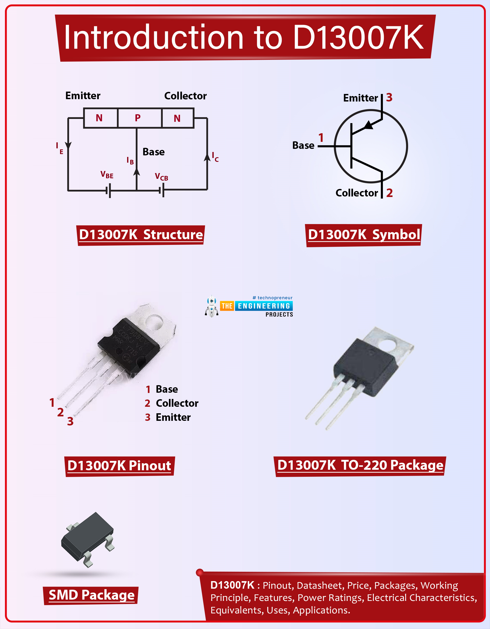
Hello Fellas! Hope you’re well today. Happy to see you around. In this post today, I’ll walk you through the Introduction to D13007K. The D13007K is an NPN power transistor mainly used for switching and amplification purpose. This device is made of silicon material and falls under the category of bipolar junction transistors. As this is an NPN transistor so here major charge carriers are electrons. Holes are major carriers in the case of PNP transistors. This is a high voltage high current capability device used in energy-saving lamps. The collector current of this chip is 8A which means it is best for loads under 8A. And the power dissipation is 80W which projects it is eligible to release 80W power during the operation of this device. The collector-base voltage is 700V and collector-emitter voltage is 400 while the voltage across the base and emitter terminals is 9V which is the voltage needed to start the transistor action and bias the device. Read this entire post till the end as I’ll document the complete Introduction to D13007K covering datasheet, pinout, power ratings, working principle, applications, and physical dimensions. Let’s dive in.

Introduction to D13007K

  • The D13007K is a power transistor that belongs to the NPN transistor family.
  • The three terminals like emitter, base, and collector make this entire device. All these terminals are connected to the external electrical circuit.
  • This is a current-controlled device because the small current at one terminal is employed to handle large current at the remaining terminals.

  • While MOSFETs are voltage-controlled devices and come with terminals like a drain, source, and gate. The gate plays the same role in MOSFETs as what base plays in bipolar junction transistors.
  • The bipolar junction transistors are mainly divided into two types one is PNP transistors and one is NPN transistors.
  • Both electrons and holes play a key role in the conductivity of bipolar junction transistors.
  • But in the case of PNP transistors holes are responsible for the major part of conductivity carried out inside the device while in the case of NPN transistors electrons play a key role in the overall conductivity inside the transistor.
  • PNP transistors are considered less efficient than NPN transistors because electrons are quicker and efficient in the conductivity process compared to holes. The mobility of electrons is far better and quicker than the mobility of holes inside the transistor.

D13007K Datasheet

It is wise to check out the datasheet of the device before incorporating it into your electrical project. The datasheet comes with the main characteristics of the device. Click the link below to download the datasheet of D13007K.

D13007K Pinout

The following figure shows the pinout diagram of D13007K. The D13007K carries three terminals known as: 1: Base 2: Collector 3: Emitter All these terminals carry different doping concentrations. Which leads to the lack of symmetry of this device. The emitter side is highly doped and the collector side is lightly doped. While the collector side is 10-times less doped than the base side.

D13007K Working Principle

  • The transistor working principle is straightforward and simple. It all initiates from the base side. When voltage is applied at the base side, it will bias the device, and as a result, the current will start flowing collector to the emitter terminal.
  • As this is an NPN transistor so here current flow is carried out from the collector to emitter terminals this is the opposite in the case of PNP transistors.
  • When voltage is applied at the base pin in PNP transitory, the current starts flowing from the emitter to the collector terminal.
  • As described earlier this bipolar device is not symmetrical. Which means if you interchange both emitter and collector side then both terminals will start working in reverse active mode and the device will stop working in forward active mode.

D13007K Power Ratings

The following table features the absolute maximum ratings of D13007K.
Absolute Maximum Ratings of D13007K
Pin No. Pin Description Pin Name
1 Collector-emitter voltage 400V
2 Collector-base voltage 700V
3 Base-emitter voltage 9V
4 Collector current 8A
5 Power dissipation 80W
6 Base current 4A
7 Operating and storage junction temperature range -55 to 150C
  • While incorporating this device into your project, make sure the ratings don’t exceed the absolute maximum ratings. Otherwise, it can damage the entire project.
  • The junction temperature and storage temperature ranges from -55 to 150C.
  • The collector-emitter and collector-base voltages are 400V and 700 respectively. And total power dissipation is 80W which demonstrates the amount of power released during the functioning of this device.
  • It is important to note that, don’t apply these ratings more than the required time, else they can affect device reliability.

D13007K Applications

D13007K is used in the following applications.
  • Used in Bistable and Astable multivibrators circuit.
  • Used in voltage regulator circuits.
  • Employed to support loads under 12A.
  • Used in electronic Ballasts.
  • Incorporated in modern electronic circuits.
  • Used in high-frequency power transform.
  • Used in a common power amplifier.
  • Used in energy-saving lights.
  • Used in the high switching power supply.

D13007K Physical Dimensions

The image below represents the physical dimensions of D13007K. By scanning those dimensions you can evaluate the space required for your component in the electrical project. That’s all for today. Thank you for clicking this read and reading it. You are most welcome to share your valuable feedback and suggestions in the section below. They help us produce quality content. You can approach me in the section below if you need any help regarding this article, I’m happy and ready to help you the best way I can. Thank you for reading this post.

Syed Zain Nasir

I am Syed Zain Nasir, the founder of <a href=https://www.TheEngineeringProjects.com/>The Engineering Projects</a> (TEP). I am a programmer since 2009 before that I just search things, make small projects and now I am sharing my knowledge through this platform.I also work as a freelancer and did many projects related to programming and electrical circuitry. <a href=https://plus.google.com/+SyedZainNasir/>My Google Profile+</a>

Share
Published by
Syed Zain Nasir