Hello everyone! I hope you all will be absolutely fine and having fun. Today, I am going to share my knowledge about Introduction to LM380. LM-380 is an audio amplifier, specially designed for the customer's power audio amplification purposes. Its designers fix its gain internally up to 34dB. In LM 380, ground reference signal is allowed by a unique input stage and the output automatically maintains its level to half of the supplied input voltage.
LM-380 has a copper lead frame. The three pins in the middle of the IC on both side, are basically the ground pins. These three pins on both sides makes it easy for the user to use this device for standard PC's. LM 380 has several different features e.g. wide supply voltage range, high peak current, lo ...
Hello everyone! I hope you all will be absolutely fine and having fun. Today, I am going to give a detailed discussion on Introduction to LF411. LF-411 is a Junction Field Effect Transistor (JFET) input Operational Amplifier (Op-amp). It is the most common module available in the market these days due to its cost efficiency. LF 411 has low input offset voltage. Input offset voltage drift is guaranteed for LF-411. A very low supply current is needed for this device. It provides higher slew rates as well as high gain bandwidth product.
Moreover, LF411 also provides lower input bias current as well as lower input offset currents. It is an 8 pin operational amplifier. The details about its pins will be discussed later. Due to its low cost and high ...
Hello everyone! I hope you all will be absolutely fine and having fun. Today, I am going to provide you the discussion on Introduction to LM393. LM-393 has two internal operational amplifiers. These are internally frequency compensated. These are specifically designed to perform their tasks using a single power supply sources. LM-393 can also perform its operations properly by using split power supply. The current drain supply does not depend upon the magnitude of the power supply.
One of the most amazing feature of LM 393 is that ground is included in its common mode input voltage. Moreover, LM 393 has a lot of features e.g. wide voltage supply ranges, a very small current drain supply, low input offset current, low input bias current, output v ...
Hello everyone! I hope you all will be absolutely fine and having fun. Today, I am going to provide a detailed discussion on Introduction to LM258. LM-258 has two internal Operational Amplifiers (Op-amps) which are frequency compensated internally. They are specially designed to perform their tasks from a single power supply source using a wide range of voltages. They can also perform different operations using split power supply. LM-258 low power supply current drain does not depend upon the magnitude of the power supply source.
LM 258 has a lot of features including high DC voltage gain, large bandwidth, different input voltage equal to power supply, large output voltage swing, common mode input voltages include ground. These were the few of m ...
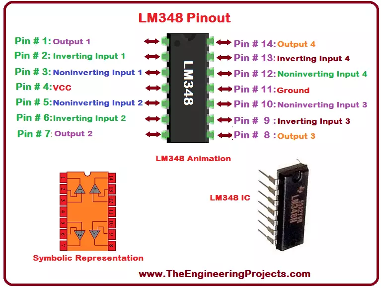
Hello everyone! I hope you all will be absolutely fine and having fun. Today, I am going to share my knowledge on Introduction to LM348. LM-348 i basically a General Purpose (GP) Operational Amplifier. It is an independent and quadruple operational amplifier. LM 348 has similar characteristics in comparison to uA741. It is an internally compensated amplifier having high gain.
LM-348 has four internal amplifiers. We can achieve isolation between these amplifiers by biasing each of the amplifier independently. This isolation can be done using different techniques e.g. layout technique. It can be used at several different places where amplifier matching is needed. LM 348 has very low supply current drain as compared to the standard 741. Moreover, I ...
Hello everyone! I hope you all will be absolutely fie and having fun. Today, I will elaborate you about Introductio to NE556 timer IC. NE-556 is a lot stable monolithic device. We can use precise delays and oscillation by using this device. NE 556 is bsically an dual version of NE 555 timer IC. Timing is provided for each function using an external capacitor and resistor. There are two internal timers which operates independently. They just share common power supply and ground. For the falling or rising wave forms we can trigger or reset the entire circuit.
The trigger level and the threshold levels are usually one third and two third respectively. We can alter both of these level by using control pin of NE-556. If the input at trigger falls bel ...
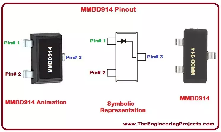
Hello everyone! I hope you all will be absolutely fine and having fun. Today, I am going to share my knowledge about Introduction to MMBD914. MMBD 914 is basically a switching diode. A switching diode has the functionality similar to the switch. Like an open switch, MMBD 914 has a high resistance for the particular applied voltage.
Switching diodes are usually used in different device e.g. ring modulation. The right switching diode can be chosen keeping in mind our requirements e.g. reverse recovery time, power dissipation and maximum peak current etc. I have also written an article on another switching diode, Introduction to 1N4148, and this my second article on switching diodes. MMBD-914 has a vey wide range of applications including high spee ...
Hello everyone! I hope you all will be absolutely fine and having fun. Today I am going to elaborate you about Introduction to L298. L-298 is an Integrated Circuit (IC) available in two type of packages now a days which will be given later. L 298 is a dual full bridge driver that has a capability to bear high voltage as well as high current. It receives basic TTL (Transistor Transistor Logic) logic levels and is able to operate the different loads such as DC motors, stepper motors, relays etc. You should also have a look at Introduction to L23D.
L-298 has two enable input to control any device by enabling or disabling it. L 298 IC is most commonly used to make motor drivers or motor controllers. These motor controllers can be controlled by any ...
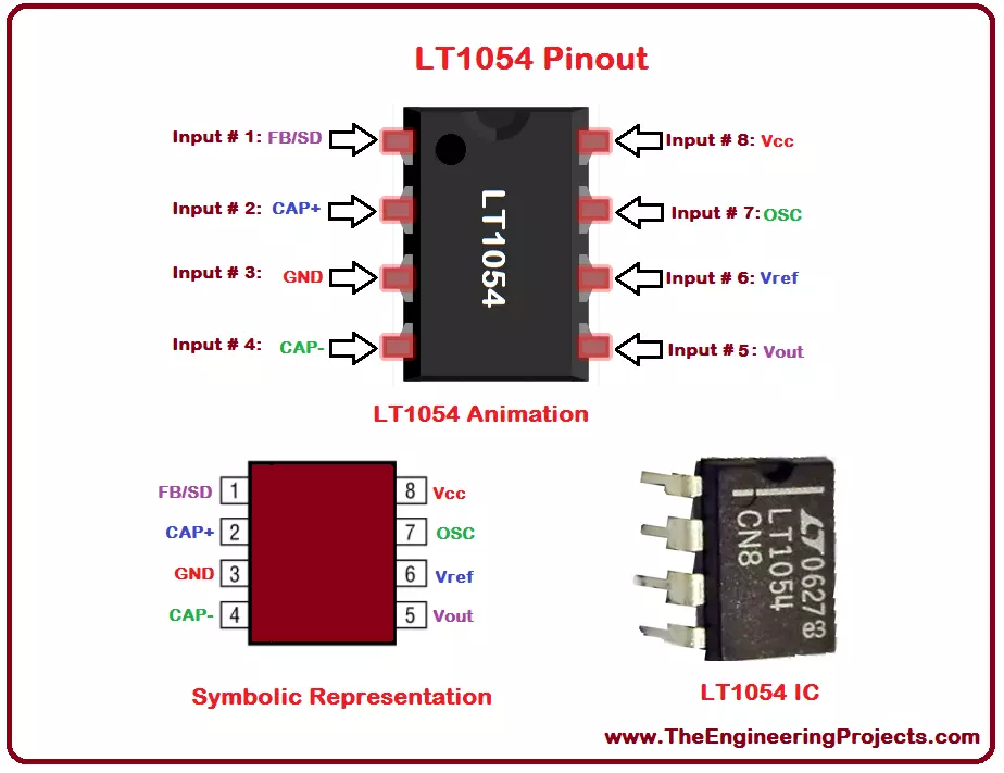
Hello everyone! I hope you all will be absolutely fine and having fun. I am going to elaborate you on Introduction to LT1054. It is a monolithic device. LT-1054 is also known as voltage regulator and bipolar capacitive voltage converter. Its mean feature is that it provides very low voltage losses as compared to the other common converters. LT 1054 also provides large output currents in comparison to general converters. It provides a voltage drop of around 1.1V while operating at 100mA.
LT 1054 provides us with a feature of regulation. This feature was not available in earlier voltage converters. We can get a regulated output just by inserting an external resistance. We can shut down LT-1054, if we ground its feedback terminal. Its internal osci ...
Hello everyone! I hope you all will be absolutely fine and having fun. Today, I am going to share my knowledge about Introduction to 74HC245. 74HC 245 is a eight (8) bit transceiver. It has three (3) output states. 74HC-245 is designed for a-synchronous transfer of data between different data buses. The external timing requirement can be reduced by the implementation of control function. You should also have a look at Introduction to 74HC595.
There are two internal amplifiers in 74HS 245. They are named as A and B. Data is transferred from A amplifier to B amplifier and vice versa. Hence two way communication is done in 74HC-245. This communication depends upon the logic level on the direction control input (DIR). Out enable pin (OE) is used to ...