Introduction to BJT (Bipolar Junction Transistor)

Hey Guys! Hope you are doing great. Today, I am going to discuss the details on the Introduction to BJT (Bipolar Junction Transistor). It is an electronic component mainly used for amplification and switching purpose. As the name suggests, it is composed of two junctions called emitter-base junction and collector-base junction. Don't confuse BJT with regular transistors. A transistor is a semiconductor device, comes with three terminals that are used for external connection with electronic circuits. A transistor is termed as a trans resistor which is used as switch or gate for electronic signals. Small signals applied between one pair of its terminals are used to control much larger signals at the other pair of terminals. Actually, transistors are divided into two categories called unipolar transistor and a bipolar transistor. Bipolar junction transistor uses two charge carries i.e. electrons and holes while unipolar transistor like FETs (Field Effect Transistors) uses only one charge carrier. I hope you are aware of another type of transistors called MOSFET. I'll try to cover each and everything related to this bipolar junction transistor, so you find all information at one place. Let's get started.

Introduction to BJT

  • Introduced in 1948 by Shockley, BJT is an electronic component mainly used for switching and amplification purpose.
  • It is composed of three terminals called emitter, base, and collector, denoted as E, B and C respectively.
  • This transistor comes with two PN junctions. The PN junction exists between emitter and base is called emitter-base junction and the PN junction exists between collector and base is called collector-base junction. Emitter-base junction is forward biased and the collector-base junction is reverse biased.
  • In the start BJTs were made from germanium, however, recent transistors are made from silicon.
  • BJT comes in two types called NPN transistor and PNP transistor.
  • It is a bipolar device where conduction is carried out by both charge carriers i.e. electrons and holes. The number of electrons diffused in the base region is more the number of holes diffused in emitter region. Electrons behave as a minority carrier in the base region.
  • Under normal conditions, when the emitter-base junction is forward biased it allows the current to flow from emitter to collector. When a voltage is applied at the base terminal, it gets biased and draws current, which directly affects the current at the other terminals.
  • BJT is called a current controlled device where small current at the base side is used to control the large current at other terminals. All three terminals of the BJT are different in terms of their doping concentrations. The emitter is highly doped as compared to base and collector.
  • The collector is moderately doped and its area is larger as compared to emitter area, allowing it to handle more power.
  • When a voltage is applied, the majority of electrons from emitter are diffused into the base where these electrons act as minority charge carriers, making the holes in the base region majority charge carriers.
  • As the base is very thin and lightly doped it cannot hold the number of electrons for too much time, allowing the electrons to diffuse from base to collector.
  • Making a slight change at the voltage applied at the base-emitter terminals can cause a significant change at the current between emitter and collector terminals.
  • This is the process used for amplification purpose.
  • When the emitter-base junction is not forward biased the amount of current at the base and collector terminal is zero, no matter how much voltage is applied at the base terminal.
  • Common-Emitter current gain is a term mostly used for BJTs. It is a ratio between collector current and base current. Similarly, a common-base current gain is defined as a ratio between collector current and emitter current. Most of the time its value is taken as unity.
  • Construction of BJT is not symmetrical in nature. The lack of symmetry of BJTs is due to the difference in doping concentration between the terminals.
  • Generally, BJTs are operated in forward-biased mode. Interchanging the emitter and collector allows the forward biased mode to change to reverse biased mode. This interchange causes a wide impact on the values of current gains, making them much smaller as they are in forward-biased mode.
  • The mode of operation where an emitter-base junction is forward biased and the collector-base junction is reverse biased is called active region.

Types of BJT

BJTs are divided into two types based on the nature and construction of the transistor. Following are two main types of the BJT.
NPN
  • NPN (negative-positive-negative) is a type of BJT where a P-doped layer of semiconductor exists between the two layers of N doped material.
  • The P doped region represents the base of the transistors while other two layers represent emitter and collector respectively.
  • NPN transistors are also called minority carrier devices because minority charge carriers at the base side are used to control large current at other terminals of the transistor.
  • The current moves from an emitter to the collector where electrons act as a minority carrier at the base side.
PNP
  • PNP (positive-negative-positive) transistor is a type of BJT where N doped semiconductor layer which acts as a base, is housed between the two layers of P doped material.
  • The base uses small base current and negative base voltage to control large current at the emitter and collector side and voltage at the collector side is larger than the voltage at the base side.
  • In PNP transistor current direction and voltage polarities are reversed as compared to NPN transistors.
  • PNP transistors work in a similar way like NPN transistor with some exception i.e. holes are diffused through the base from an emitter and are collected by the collector.
  • This transistor is rarely used for applications as conduction carried out by the movement of electrons is considered fast and holds more value as conduction by movement of holes.

Regions of Operations of BJT

Bipolar junction transistors come with different regions of operation. These modes of operations set a tone for current flowing from emitter to collector.
Forward Active Mode
  • BJT comes with two junctions called emitter-base junction and collector-base junction. Emitter-base junction is forward biased and the collector-base junction is reverse biased.
  • For amplification purpose, most of the transistors come with high common emitter current gain which shows the exact current and power gain required for amplification purpose.
  • The collector-emitter current is largely dependent on the base current where small current at the base side is used to control the large current at the emitter and collector side.
Reverse Active Mode
  • By interchanging the emitter and collector, transistor goes from active mode to reverse active mode.
  • Most of the transistors are designed to afford high current gain, but reversing the role of emitter and collector makes the current gain very small as compared to forward biased region. This type of mode is rarely used unless a failsafe condition is required.
Saturation
  • BJT exhibits saturation mode when both junctions are forward biased. This mode of operation is referred as a closed circuit which allows a large amount of current flowing from emitter to collector side.
Cut-off
  • When the emitter-base junction is not forward biased, the transistor is said to have in the cut-off region where collector current and base current will be zero, no matter how much voltage is applied at the base terminal.

Three Basic Configurations of BJT

BJT is a current controlled device which is mainly used for amplification and switching purpose. There are three ways to connect this device with external electronic circuits called: 1. Common Base Configuration 2. Common Collector Configuration 3. Common Emitter Configuration The nature of the current being controlled at the output is different for different configurations.
Common Base Configuration
  • Common base configuration is a configuration where the common base is shared between input and output signal.
  • Voltage is applied at the emitter-base junction and corresponding output signal is obtained at the output across the base-collector junction.
  • The base voltage is connected to some reference voltage or can be grounded in some cases with the intention of making common base between input and output signals.
  • Following figure shows the circuit diagram of common base configuration.
  • Current at the emitter side is quite large, where electrons are diffused into the base terminal. These electrons make a pair with some holes present in the base, while most of them leave the base and are collected by the collector.
  • This type of transistor comes with remarkable high voltage characteristics which don't make it an ideal choice for many applications. In this configuration, an output and input voltage is in line with each other. The input characteristics of this transistor are quite identical to forward biased diode while output characteristics are similar to a regular diode and come with a high output to input resistance ratio.
  • Common base current gain is a very important factor used in this configuration which is a ratio between collector current and emitter current. It is denoted by a alpha.
  • a = Ic/Ie
  • The alpha value ranges between 0.95 to 0.99, however, most of the time its value is taken as unity. High-frequency response of common base configuration makes it an ideal choice for single stage amplifier.
Common Collector Configuration
  • This configuration is also known as voltage follower where the input is applied at the base terminal and output is taken from emitter terminal.
  • This configuration is mainly used for impedance matching as the input impedance of this configuration is very high while output impedance is very low.
  • Common collector configuration is termed as non-inverting amplifier where output signal and an input signal are in phase with each other.
  • The current gain of this transistor is very large because the load resistance is at the receiving end of both collector current and base current, making it a suitable for amplification purpose.
  • Hence very little voltage gain, around unity, can help in producing very large current gain.
  • Following figure shows the circuit diagram of common collector configuration.
Common Emitter Configuration
  • This configuration is widely used in transistor based amplifier, where an input signal is applied between emitter and base while the output is taken from emitter and collector.
  • This configuration comes with highest current and power gain which makes it an ideal choice for amplification. Input impedance is connected to forward biased PN junction which shows low value while output impedance is connected to reverse biased PN junction which shows high value.
  • Most of the transistors generally come with common emitter configuration because this exhibits the ideal power and current required for amplification purpose.
  • Common emitter configuration is termed as inverting amplifier circuit where an input signal is out-of-phase with the output signal.
  • Following figure shows the circuit diagram of common emitter configuration.
 
  • The common emitter current gain of this transistor is very large as compared to a current gain of common base configuration which is a ratio between collector current and base current. It is denoted by ß beta which is the measure of current being amplified.
  • ß = Ic/Ib
  • Output current at the collector and emitter side is highly dependent on the current at the base side.
  • Current at the emitter side is the sum of current at the base and collector side because emitter side is highly doped as compared to base and collector.
  • Ie = Ib + Ic
  • When the voltage is applied at the base terminal it triggers the electrons reaction which forces the electrons to move towards the collector side.
  • Any small change at the voltage applied at the base terminal results in a very large change at the current obtained at the collector side.

Pros of BJTs

  • Bipolar junction transistor comes with a large amplification factor.
  • This type of transistor provides a better voltage gain.
  • This transistor comes with a capability of operating in four regions i.e active region, reverse mode, saturation and cut-off region.
  • BJT provides a better responese at higer frequiencies.
  • BJTs also act as a switch.

Cons of BJTs

  • BJT is very sensitive to heat and produces noise is some cases.
  • The switching power of BJTs is very low as compared to unipolar transistors like FETs.

Applications

  • BJTs come with two major applications called amplification and switching.
  • They are the building blocks of most of the electronic circuits, especially where audio, current or voltage amplification is required.
  • NPN transistors are preferred over PNP transistors for amplification purpose because conduction carried out through mobility of electrons is better than conduction through mobility of holes.
That's all for today. I have tried my best to break down each and everything related to BJTs so you can digest the main concept easily. In case you are unsure or have any question you can ask me in the comment section below. I'd love to help you according to best of my expertise. Feel free to keep us updated with your valuable suggestions, they allow us to give you quality work. Thanks for reading the article.

Introduction to 2n6547

Hey Fellas! Hope you are doing great and having fun in your lives. We always try to keep you updated with useful information that resonates with your needs and expectations so you can grow and excel in your relevant field. I am back to give you a daily dose of useful information that may help you resolve your queries and problems related to engineering and technology field. Today, I am going to unlock the details on the Introduction to 2n6547. It is an NPN bipolar junction transistor that comes with high voltage and current capability and fast switching speed, mainly used in switched mode power supplies and flyback and forward single transistor low power converters. I'll try to cover each and everything related to this NPN transistor, so you don't need to go anywhere and find all information in one place. Let's dive in and explore what is this about and what are its main applications?

Introduction to 2n6547

  • 2n6547 is an NPN bipolar junction transistor that comes with high voltage and current capability and fast switching speed, mainly used in switched mode power supplies and flyback and forward single transistor low power converters.
  • It comes in a TO-3 metal case and is an ideal choice for industrial and switching applications from single and three-phase mains.
  • This NPN transistor is a bipolar junction transistor where conduction is carried out by the movement of both charge carriers, i.e electrons, and holes, however, main charge carriers are electrons.
  • It mainly consists of three terminals called emitter, base, and collector.
  • All three terminals are different in terms of size and doping concentration. An emitter is highly doped as compared to base and collector while a base is lightly doped.
  • When a voltage is applied at the base terminals, it triggers the electron reaction which draws current.
  • Small base current is used to control large current at the emitter and collector side.
  • Electrons play an important role in maintaining the bridge between emitter and collector of this transistor.
2n6547 Pinout
Following figure shows the pinout of 2n6547
  • This transistor is basically a current operated device where small current at the base side is used to control the large current at the emitter and collector side.
  • The ability of base current to control large currents is used for amplification purpose.
  • This transistor is a bipolar current controlled device which is different than JFET that is a unipolar voltage controlled device.
Circuit Symbol of 2n6547
Following figure shows the circuit symbol of 2n6547.
  • The base of the transistor is more positive than the emitter while the voltage at the collector side is more than base voltage.
  • Current at the emitter side is equal to the sum of current at the base and collector side.
  • As it is an NPN transistor, it sources the base current to the transistor.
  • The measure of a number of electrons that pass from base to collector is called transistor efficiency.
  • The base is lightly doped and the emitter is heavily doped that will allow the electron to move from the emitter to base more than it will allow the holes from base to emitter.
  • Transistors always operate in forward biased mode. If we interchange emitter and collector and makes it reverse biased, then the value of alpha and beta will be much lesser than they will be in forward biased mode.
  • Forward current gain is represented by beta ß, which is an important factor for amplification purpose. It is a ratio between collector current and base current and its value ranges between 20 to 1000, however, its standard value is 200.
  • Current gain is another important factor which is a ratio between collector current to the emitter current and it is denoted by alpha a. Value of alpha ranges between 0.95 to 0.99, however, most of the times alpha value is considered as a unity.
Absolute Maximum Ratings of 2n6547
Following figure shows the absolute maximum ratings of 2n6547.
  • It is important to note that these are the stress ratings. If these stress ratings are exceeded above absolute maximum ratings, they can damage the device at large and affect the quality of the component.
  • If these stresses are applied for a maximum period of time, they can affect the reliability of the component.
  • Take strict measures and follow international protocols while dealing with this components, otherwise, they can affect the project you are picking this component for.
Applications
  • It is mainly used in switched mode power supplies.
  • Flyback and forward single transistor low power converters make use of this device as it exhibits high voltage and current capability.
  • This transistor is an ideal choice for switch mode applications ranges between 115 to 220 V.
  • Inductive circuits where fall time plays an important role, are equipped with this transistor.
  • For industrial purpose, it is used for motor drive control.
That's all for today. This transistor comes with electrons as majority carriers, different than PNP transistor that comes with holes as majority carriers. I hope you have found this article useful. However, if still you feel skeptical or have any question, you can ask me in the comment section below. I'd love to help you according to best of my expertise. Keep up updated with your valuable feedback and suggestions, as they allow us to give you quality work that meets your requirements. Thanks for reading the article. Stay Tuned!

Introduction to 2n4400

Hey Fellas! I hope you are doing great and having fun. We love when you keep coming back again and again for what we have to offer that resonates with your needs and requirements. I am back to give you a daily dose of useful information so you can excel and grow in your relevant field without much effort. Today, I am going to unlock the details on the Introduction to 2n4400. It is an NPN (negative-positive-negative) bipolar transistor which is mainly designed for general purpose amplification and switching applications. I'll cover each and everything related to this transistor, so you get all information in one place without roaming around on the internet. Let's get started.

Introduction to 2n4400

  • 2n4400 is an NPN general purpose bipolar junction transistor which is mainly used for amplification and switching applications.
  • It is mainly composed of three terminals called emitter, base, and collector, where small current at the base side is used to control large current at the emitter and collector side.
  • This NPN transistor consists of two N doped layers which cover the one P doped layer. The P terminal shows the base of the transistor while other two terminals show collector and emitter respectively.
  • Most of the old transistors were made of germanium. However, new transistors are made from silicon.
  • When a voltage is applied at the base terminal, it triggers electron reaction, gets biased, draws current which is then used to control large current at the collector and emitter side.
  • All three terminals are different in terms of size and doping concentration. An emitter is highly doped as compared to collector and base while a base is lightly doped. However, a voltage at the collector side is more than the voltage at the base side.
  • Actually, movement of electrons acts like a bridge between emitter and collector.
  • 2n4400 is also referred as bipolar junction transistor where conduction is carried out by the movement of electrons and holes, however, majority charge carriers are electrons.
  • You must look at the introduction to diode which plays a vital role in the construction of transistor.
2n4400 Pinout
Pinout of the 2n4400 is shown in the figure below.
  • The base controls the number of electrons and draws current which is then used to control large current at the other terminals. This process is used for amplification purpose.
Circuit Diagram of 2n4400
Following figure shows the circuit diagram of the 2n4400.
  • Emitter current is equal to the sum of base and collector current because doping concentration of emitter is more than both collector and base.
  • This transistor can be configured into three configurations called common base configuration, common collector configuration, and common emitter configuration. Common emitter configuration is mostly used for the amplification purpose because it provides the required power and voltage for the amplification purpose.
  • Forward current gain is an important feature in this NPN transistor, which is also called amplification factor that defines the measure of current being amplified. It is called beta ß, and it is a ratio between collector current and base current. Beta value is a ratio between two currents so it exhibits no unit.
  • Beta value ranges between 20 to 1000. However, standard value of beta is 200.
  • Current gain is another important factor which is called alpha a and it is a ratio between collector current and emitter current. Alpha value ranges between 0.95 to 0.99. However, most of the time alpha value is taken as unity.
  • Transistors always operate in forward biased mode. If we interchange emitter and collector and makes it reverse biased, then the value of alpha and beta will be much lesser than they will be in forward biased mode.
  • In the ON state current will flow from emitter to collector and free movement of electrons from the base side is used to control the current between emitter and collector.
Absolute Maximum Ratings
Following figure shows the absolute maximum ratings of 2n4400
  • It is important to note that, these are the stress ratings, which if exceed from the absolute maximum ratings, can damage the device quality and overall functionality of the device.
  • It is recommended to apply these stress ratings for the specific period of time given by the manufacturer. If these ratings are applied for a maximum period of time they can affect the device reliability.
Applications
  • This NPN transistor is widely used for general purpose amplification and switching purpose.
That's all for today. I have tried my best to cover each and everything related to this amplification transistor. However, if still you feel skeptical or have any question you can ask me in the comment section below. I'd love to help you based on my best of my knowledge and expertise. I'd suggest you have a look at PNP transistor where holes are majority carriers, different than NPN transistor where electrons are majority carriers. Feel free to provide us your valuable feedback and suggestions, they allow us to give you quality work that matches with your relevant field and helps you resolve your queries. Thanks for reading the article. Stay Tuned!

Introduction to 1n751a

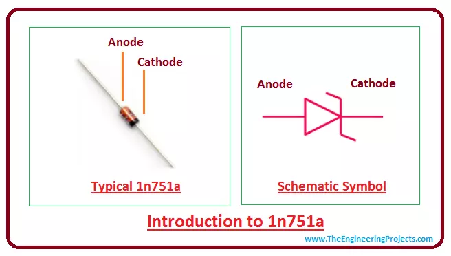
Hey Friends! We welcome you on board. I am back to give you daily dose of information. Electronic components play an important role in the designing and working of electronic projects. Today, I am going to unlock the details on the Introduction to 1n751a. It is a zener diode, also known as highly reliable voltage regulator, which is mainly used in industrial, commercial, entertainment and computer applications. It is slightly different than regular diode, as regular diode conducts in only one direction while zener diode can conduct in both directions. I will discuss every aspect related to this zener diode, so you don't need to go anywhere and find all information in one place. Let's dive in and explore, what is it about and what are its main applications?

Introduction to 1n751a

  • 1n751a is a zener diode which is also referred as highly reliable voltage regulator, mainly used in industrial, commercial, entertainment and computer applications.
  • It comes with a very sharp reverse characteristics, which makes it an ideal choice for voltage stabilization applications.
  • This zener diode is a p-n junction diode which is capable of conducting in both directions i.e. forward direction and reverse direction.
  • However, making it operate in reverse biased condition is little bit tricky because reverse breakdown voltage must be achieved in order to operate it in reverse biased condition.
  • One important feature that makes this zener diode ahead of regular diode is that voltage drop across the zener diode doesn't change over a wide range of voltages, which makes it suitable and highly effective for voltage regulation applications.
  • This zener diode works in breakdown voltage and is an ideal choice for generating reference voltage.
  • Most of the electronic circuits are equipped with this zener diode because it prevents them from over voltage.
  • This zener diode comes with 1.5 forward voltage at 200mA and votlage tolerance appears to be 5%. And reverse leakage current is 1 µA at 1 V.
  • It features very effective working characteristic and comes with a power of 500 mW.
Working of 1n751a
  • Working of this zener diode is quite identical to normal diode with one exception - it conducts in both directions.
  • This zener diode acts like a normal diode in forward biased condition.
  • It will only allow the conduction in the reverse direction when reverse voltage reaches to the breakdown voltage, allowing the current to flow from cathode to anode.
  • Over a wide range of applied voltage, current reaches to maximum point and stabilizes itself after a certain amount of time, making it suitable for using as a voltage stabilizer.
  • Zener breakdown effect is the main cause of voltage breakdown. However, it can also occur due to impact ionization. Both mechanism come into play at 5.5 V and come with same feature and don’t need different circuitry for working efficiently. However, temperature coefficient is the main feature where both mechanism differ. Zener effect shows negative temperature coefficient while impact ionization shows positive temperature coefficient. Both effects cancel each other at 5.5 V, helps zener diode achieving the most stable state over a wide range of temperatures.
Applications
This zener diode comes with a lot of applications and used in electronic circuits in different forms ranging from voltage regulator to waveform clipper to voltage shiftier. However, mainly it is used for voltage regulator. Let's discuss, how it is used in different form in electronic circuits.
1. Voltage Regulator
  • When zener diode is connected in parallel with the voltage using reverse biased mode, it will be capable of starting conduction when voltage equals to a breakdown voltage.
  • You can see from the figure above that source voltage is applied in parallel with the diode that helps in decreasing the output voltage from its input, keeping the breakdown voltage constant over a wide range of source voltage.
  • Constant breakdown voltage takes a vital part in maintaining the stable output voltage, making it unable for input voltage to effect the output voltage.
2. Waveform Clipper
  • Zener diode shows a different behavior when it is connected in series.
  • It acts as a waveform clipper when connected in series, allowing the waveform to clip from both ends of the cycle i.e. positive end and negative end of the cycle.
  • High voltage spikes that can occur at the end of output voltage can also be prevented with the use of zener diode, helping in reshaping the output signal.
3. Voltage Shifter
  • Voltage shifting is another feature in which zener diode is good at.
  • When it acts as a voltage shifter, it reduces the amount of output voltage equal to the breakdown voltage.
That's all for today. I hope you have enjoyed the article. However, if still you feel skeptical or have any question, you can approach me in the comment section below. I'd love to help you based on best of my knowledge and expertise. Feel free to keep us updated with your suggestions, as they allow us to give you quality work that resonates with your needs and expectations. Thanks for reading the article. Stay Tuned!

Introduction to DG408

Hello Friends! I aspire you a very happy life. Whenever you come over and visit our site, we feel happy to keep you updated with relevant information that can help resolve your questions and queries. Most of the hobbyist and students take interest in electronic devices and components that are the building blocks of electronic projects. Today, I am going to uncover the details on the Introduction to DG408. It is a multiplexer, also known as data selector, that comes with 8 channel input, in which of one the eight inputs is connected to the common output for the transmission of data over network in a specific bandwidth and time. It is an ideal choice for audio signal routing and single supply system. I'll discuss each and everything related to this multiplexer so you don't need to go anywhere and find all information in one place. Let's dive in and explore what is this about and what are its main applications?

Introduction to DG408

  • DG408 is a multiplexer, also called as data selector, that comes with 8 channel input, in which of one the eight inputs is connected to the common output for the transmission of data over network in a specific bandwidth and time.
  • Multiplexing helps in the transmission of individual data using same transmission channel.
  • DG408 allows to communicate with number of input signals and picks one of the input signals as an output signal. It is very helpful in the making of graphics controllers and CPUs (digital semiconductors).
  • It is embedded with an array of 8 Analog switches that are equally matched for bidirectional signals, Enable input for device selection, Voltage reference for logic threshold, Compatible digital decode circuit for channel selection.
  • Low power dissipation is an important feature of this device that makes it efficient and suitable for remote instrumentation and battery operated applications.
  • Additional improvements has been added in the device using silicon-gate CMOS process that allows it to withstand absolute maximum ratings up to 44 V.
  • A multiplexer is also referred as multiple input, single output device that allows to incorporate with number of signals at a time.
  • It comes with a guaranteed matching between channels (8O Max) and allows to conduct in both direction equally well.
  • This is a low on-resistance device that offers guaranteed low charge injection and comes with low input off leakage current around 5nA.
  • The voltage range on which this device can operate is 5 V to 30 V with single supply and 5 V to 20 V with dual supplies.
  • One important feature that makes this device ahead from its counterparts is using single channel for each data source instead of using separate channel for each data source.
  • It is achieved by connecting single output of the multiplexer to the single input to the demultiplexer. In terms of cost, this feature is very valuable and economical because it refrains us from spending more money for separate channel for each data source.
  • Most of the time, multiplexer is connected with demultiplexer into a single unit which is referred as multiplexer. Both ends of the transmission link require both circuit elements because transmission is required in both direction for most of the communication system.
DG408 Pinout
Following figure shows the pinout of this multiplexer DG408.
  • The eight analog switches, shown in the figure above, are bilateral, that can be equally matched for AC signals.
  • The on-resistance variation is very low that is associated with analog signals over a 5V range.
  • Enable input is used for device selection and digital decode circuit is used for channel selection.
  • Voltage reference is used for logic threshold.
Features of DG408
  • Pin-Compatible Plug-In Upgrades for Industry Standard DG408
  • Matching Between Channels is assured, 8O Max
  • On-Resistance Flatness is guarantted, 9O Max
  • Low Charge Injection is guarantted, 15pC Max
  • Low On-Resistance, 100O Max
  • Input Leakage, 5nA Max at +85°C
  • ESD Protection >2000V per Method 3015.7
  • Low Power Consumption, 1.25mW Max
  • Rail-to-Rail Signal Handling
  • Digital Input Controls TTL/CMOS Compatible
Absolute Maximum Ratings
Following figure shows the absolute maximum ratings of DG408
  • It is important to note that singles will be restricted by internal diodes if they try to exceed from V+ and V- values.
  • All terminals can be soldered to circuit board.
Truth Table
Following figure shows the truth table of DG408.
  • Truth table shows the value of Boolean variable for each switch status.
  • There are total 8 inputs across which we can obtain output that resonates with the value of one the Boolean variables.
  • This truth table is important in depicting the status of On switch for input value.
Advantages of DG408
This multiplexer comes with a number of advantages including:
  • Reduced Glitching
  • Reduced switching errors
  • Improved data throughout
  • Low power consumption
  • Low power dissipation
  • Wide supply range
  • Increased ruggedness
Applications
This multiplexer is widely used in number of applications, specially where transmission of data is required. Some of the main applications are given as follow:
  • Data acquisition systems
  • Single supply systems
  • Audio signal routing
  • ATE systems
  • Medical instrumentation
  • Sample and hold circuits
  • Battery powered systems
  • Remote instrumentation
  • Test equipment
  • Analog Selector Switch
  • Guidance and control system
That's all for today, I hope you have enjoyed to article. I always try my best to give you most relevant information that meets with your needs and requirements so you can grab the main idea explained in the article, without much effort. We love when you keep us updated with your suggestions, they allow us to give you quality work that helps you resolve your problems related to engineering and technology. Thanks for reading the article. Stay Tuned!

Introduction to BC182L

Hi Guys! We welcome you on board. Electronic components play an important role in the designing and working of electronic projects. I have already discussed a number of articles on electronic components covering transistors, MOSFET, and FETs. I am going to continue the thread relating to transistors, because they are the building blocks for amplification and switching purpose. Today, I am going to cover the details on the Introduction to BC182L. It is an NPN (negative-positive-negative) general purpose bipolar transistor which is mainly used for switching and amplification purpose for the low demanding workloads. I'll try to highlight the main features of this component, so you can grab the main concept, what is this about and what are its main applications? Let's get started.

Introduction to BC182L

  • BC182L is an NPN bipolar general purpose transistor which is mainly used for switching and amplification purpose at a collector current to 100mA.
  • It is a bipolar transistor, means conduction is carried out by the movements of both charge carriers i.e electrons and holes, however, majority charge carriers are electrons.
  • It consists of three terminals called emitter, base, and collector. Each terminal comes with a specific function associated with it.
  • BC182L is an NPN transistor, where a base is positive with respect to emitter and voltage at the collector side is more than base. Emitter, base, and collector are different in terms of size and doping concentration.
  • An emitter is highly doped as compared to collector and base, while a base is lightly doped.
  • It is a current controlled device where small current at the base side is used to control large current at the emitter and collector side.
  • When a voltage is applied at the base terminal, it gets biased and draws current which is used to control large current at the other terminals.
  • The emitter emits the electrons which are then collected by the collector; the base is mainly used for controlling the number of electrons.
  • Actually, free movement of electrons acts like a bridge between emitter and collector.
  • Transistor is nothing but a combination of diodes joined back to back.
BC182L Pinout
BC182L mainly consists of three terminals. 1. Emitter 2. Collector 3. Base
  • Movement of electrons plays an important role in the conductivity of the transistor.
  • And electron reaction starts when a voltage is applied at the base terminal.
Circuit Diagram of BC182L
Following figure shows the circuit diagram of the BC182L.
  • We can see from the figure, emitter current is equal to the sum of base and collector current. Because emitter is bigger than collector and base in terms of doping concentration.
  • BC182L is an NPN transistor and it will source the base current to the transistor.
  • The measure of a number of electrons that pass from base to collector is called transistor efficiency.
  • The base is lightly doped and an emitter is heavily doped that will allow the electron to move from the emitter to base more than it will allow the holes from base to emitter.
  • Forward current gain plays an important role for amplification purpose. It is called beta, denoted by ß, and it is a ratio between collector current and base current. Beta value ranges between 20 to 1000, however, it has standard value 200.
  • Current gain is another important factor which is called alpha, denoted by a, and it is a ratio between collector current and emitter current. Alpha value ranges between 0.95 to 0.99 however, most of the time alpha value is considered as a unity.
  • Almost all the transistors operate in forward biased mode. If we interchange emitter and collector and makes them reverse biased, then the value of alpha and beta will be much lesser than they will be in forward biased mode.
  • This NPN transistor comes with electrons as major charge carriers while PNP transistor comes with holes as majority charge carriers.
Absolute Maximum Ratings
Following figure shows the absolute maximum ratings of this component.
  • These are the stress ratings, which if exceeded from the absolute maximum ratings, can damage the device severely and affect the overall quality of the component.
  • If these stresses are applied for the extended period of time, they can affect the reliability of the device.
  • In order to avoid any loss or damage, it is recommended to follow the operating conditions given by the manufacturer. Taking measures and following proper protocols in the early stage of your project can save you both cost and time.
  • I'd suggest you have a look at 2n3903 if you require different ratings as compared to this transistor.
Applications
  • It is mainly used for amplification and switching purpose.
  • Audio and signal processing makes use of this transistor.
That’s all for today. I have tried my best to explain each and everything regarding this BC182L transistor. However, if you still find any difficulty in understanding the concept of this transistor, you can ask me in the comment section below. I’d love to help you in this regard. Thanks for reading the article. Stay tuned!

Introduction to 2n5551

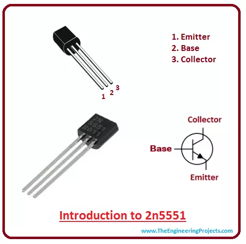
Hi Fellas! I hope you all are doing great and having fun with your lives. We always strive to give you quality work that resonates with your needs and allows you to come back again and again. I am back to give you a daily dose of useful information so you can excel and grow in your relevant field. Today, I am going to discuss the details on the Introduction to 2n5551. It is an NPN (negative-positive-negative) bipolar junction transistor BJT which is mainly designed for gas discharge display drivers and general purpose amplification. I'll try to cover each and every aspect related to this transistor so you don't need to go anywhere and you find all information in one place. You can also have a look at Introduction to 2n5401 which is a complementary PNP transistor of this NPN 2n5551 transistor. Let's dive in and explore what is it about and what are its main applications?

Introduction to 2n5551

  • 2n5551 is an NPN bipolar junction transistor which is mainly used for general purpose amplification and gas discharge display drivers.
  • It consists of three terminals known as the emitter, base, and collector and comes in a TO-92 package.
  • Unlike FETs, this NPN transistor is a current controlled device where small current at the base side is used to control large current at the emitter and collector side.
  • As it is an NPN transistor so the base will be positive with respect to the emitter.
  • It features high breakdown voltage, low leakage current, capacity and beta value which are very useful over a wide range of current.
  • Movement of electron plays an important role in defining the conducting nature of any transistor. This NPN transistor is known as BJT (bipolar junction transistor) because conduction is carried out by both electrons and holes but majority charge carriers are electrons.
  • Whenever a voltage is applied at the base, it gets biased and controls the current at the emitter and collector side.
  • The emitter emits the electrons which are collected by the collector. A base is used to control the number of electrons.
  • The ability of the base to control the number of electrons is used for amplification purpose.
2n5551 Pinout
2n5551 is an NPN transistor, also known as a current controlled device which contains three terminals as follow. 1. Emitter 2. Base 3. Collector
  • It is different than JFET which is a unipolar transistor, also known as a voltage controlled device.
  • Transistor action is triggered when a voltage is applied at the base side which allows the free movement of electrons.
  • Movement of free electrons is nothing but a bridge between emitter and collector.
Circuit Diagram of 2n5551
The circuit diagram of 2n5551 is shown in the figure below.
  • The emitter current is equal to the sum of collector and base current.
  • The voltage at the base side must be positive with respect to the emitter for current flow from emitter to collector.
  • Forward current gain is an important factor in determining the characteristics of this transistor. It is called Beta and represented by ß. It is a ratio between collector current to the base current. As it is a ratio between two current so it exhibits no unit.
  • Beta value is also known as amplification factor which determines the value of current being amplified.
  • Beta value ranges between 20 to 1000 but it comes with a standard value of 200.
  • The current gain of the transistor is another important factor which is called alpha and represented by a. It is a ratio between collector current and emitter current. Alpha value ranges between 0.95 to 0.99 but most of the time its value is taken as unity.
  • The NPN transistor mainly consists of two diodes combined back to back.
Absolute Maximum Ratings
Following figure shows the absolute maximum ratings of 2n5551.
  • Collector-Emitter and Collector-Base voltages are 160 and 180 respectively.
  • And maximum power it can dissipate is 630 mW.
  • These are the stress ratings which if exceeded from absolute maximum ratings, can damage the device at large.
  • Similarly, if stresses are applied for an extended period of time, they can affect the overall reliability of the device.
Difference between NPN and PNP Transistors
  • The main difference between these two transistors is the type of charge carrier.
  • Electrons are main charge carriers in case of NPN transistors while holes are main charge carriers in case of PNP transistors.
  • Most of the experts prefer NPN transistors for most of the applications because they consider conduction through electrons is better than conduction through holes.
Applications
  • 2n5551 comes with high breakdown voltage and is mainly used in gas discharge display drivers.
  • General purpose amplification is another feature of this NPN transistor which makes it an ideal choice for most of the professionals.
That's all for today. I hope you have found this article useful. However, if you have any question you can ask me in the comment section below. I'd love to guide you according to best of my expertise. We really appreciate if you keep us updated with your feedback and suggestions, they allow us to give you quality work. Thanks very much for reading the article. Stay Tuned!

Introduction to 1n5819

Hi Guys! We always feel happy when you come over to browse useful information that meets with your needs and requirements. Electronic components used in electronic industry are the backbone of recent technology that make our lives easy and help us get rid of the most conventional ways of running electronic projects. Today,  I am going to discuss the details on the Introduction to 1n5819. This is a metal to silicon power diode, also termed as Schottky Rectifier, that applies Schottky Barrier Principle. It is mainly used as rectifiers in high frequency low voltage inverters, polarity protection diodes and free wheeling diodes. I'll try to cover each and everything related to this transistor so you don't need to go anywhere and find all information in one place. Let's dive in and unlock the properties of this diode.

Introduction to 1n5819

  • 1n5819 is a metal to silicon power diode that applies Schottky Barrier Principle. It is also referred as Schottky Rectifier(named after Scientist Walter H. Schottky), surface barrier diode, hot electron diode or hot carrier diode.
  • This diode is mainly used as a rectifier in many devices including high frequency low voltage inverters, polarity protection diodes, free wheeling diodes and radio frequency applications.
  • It is little bit different than normal PN junction diode where metal like platinum or aluminium are used in place of P-Type semiconductor.
  • In Schottky diode, semiconductor and metal joined together, forming a metal-semiconductor junction where semiconductor side acts as an cathode and metal side acts as a anode.
  • When metal-semiconductor junction formed between metal and semiconductor, they result in depletion layer also referred as Schottky barrier.
  • Schottky comes with low stored charge and exhibits low power loss and high efficiency mechanical characteristics.
  • It is manufactured in such a way that all external surfaces are corrosion resistant and terminals are easily solderable where current flows in one direction only and it stops the current flowing in other direction.
  • Maximum temperature it can withstand for soldering purpose is 260 °C.
  • Guard ring die construction gives it transient protection and high surge capability.
  • The power drop occurred in this diode is lower than PN junction diodes.
  • The Schottky diode is a semiconductor diode that comes with fast switching applications and it pertains to less unwanted noise as compared to PN junction diode which makes it an ideal choice for most of the switching applications.
  • When voltage is applied across the diode terminals, current starts to flow which results is small voltage drop across the terminals.
  • The voltage drop in this diode lies around 0.15 to 0.45 which is very low as compared to regular diode where voltage drop lies between around 0.6 to 1.7 V.
  • The lower voltage drop results in higher efficiency and higher switching speed.
  • The voltage drop is actually referred as a voltage required to turn on the diode.
  • The voltage required to turn on the germanium is same as Schottky diode, but germanium diodes are not used in most of the applications because they feature very less switching speed as compared to germanium diode.
How Schottky Diode 1n5819 Works
  • Working of Schottky diode is slightly different than normal PN junction diode where P-Type semiconductor is replaced by metal.
  • When metal and semiconductor are joined together, they shape a metal-semiconductor junction which allows the flow of electron from higher energy level to lower energy level.
  • As the electrons available in N-Type semiconductor exhibit more energy and start flowing from semiconductor to the metal region.
  • We know when atom loses an electron, it results in positive ion and when atom gains electrons it results in negative ion.
  • Similarly, when N-Type semiconductor loses electron, it clothes positive charge on it and the electrons that go to the metal allow it to cloth negative charge on it.
  • The positive and negative charges appearing on the metal and semiconductor region are nothing but the depletion region.
  • The electronic width available in the n-type semiconductor is much larger than the electronic width that allows the electron to move from semiconductor to the metal.
  • Basically built-in-voltage houses inside the semiconductor that can be seen by the conduction bands when electrons try to move to the metal region.
  • In order to move electrons from semiconductor to the metal region, the positional energy of the electrons must be greater than the built-in-voltage.
  • We are referring unbiased Schottky diode where only small number of electrons pass from semiconductor to metal region because built-in-voltage creates a barrier which refrains the large movement of electrons from semiconductor to the metal region.
Absolute Maximum Ratings of 1n5819
Following figure shows the absolute maximum ratings of 1n5819.
  • It is important to note that these are the stress ratings, which if exceed from absolute maximum ratings, can damage the device severely.
  • Similarly, if stresses are applied for extended period of time, they can effect the reliability of the device.
Comparison between Schottky Diode and PN junction Diode
  • There are number of differences between Schottky diode and PN junction diode. The Schottky diode is a uni-polar device because conduction is carried out by the movement of electrons only. Conduction through holes is very negligible as compared to conduction through electrons.
  • PN junction diode is a bipolar device where conduction is carried by the movement of both charge carriers i.e. electrons and holes.
  • In Schottky diode, the reverse breakdown voltage and depletion region is very small or negligible as compared to silicon PN junction diode.
  • Similarly, the voltage drop across Schottky is very low as compared to PN junction diode which makes it suitable for many switching applications.
Applications
Schottky diodes come with a number of applications including
  • General purpose rectifier
  • Radio frequency applications
  • Detect signals and power supplies
  • Logic Circuits
  • Polarity protection diodes
  • Free wheeling diodes
That's all for today. I hope you have enjoyed the article. We love to keep you updated with relevant information that helps you resolve your questions and queries. However, if you feel skeptical or have any question you can approach in the comment section below.I'll get back to you as soon as possible and help you with best of my expertise. Thanks for reading the article. Stay Tuned!

Introduction to TIP120

Hi Friends! We welcome you on board. Electronic industry is already filled with a number of devices and components that help ease the daily life of a common man. However, there is always much room for innovation in the electronics industry when it comes to facilitating the customers. When there comes a requirement for switching and amplification, there is a need for transistors. Today, I am going to unlock the details on the Introduction to TIP120. This is an NPN Darlington transistor which is mainly used for general purpose amplification and medium power switching applications. It comes with a Darlington pair in which two transistors are connected in such a way, the current amplified by the one transistor is being amplified further by the other transistor. This configuration features much higher current gain as compared to if each transistor is taken separately. Before we move on, you must have a look at BJT (Bipolar Junction Transistor) that I have updated recently. Let's get started.

Introduction to TIP120

  • TIP120 is an NPN Darlington transistor which is mainly used for general purpose amplification and medium power switching applications.
  • It mainly consists of an emitter, base, and collector which are the basic parts of any transistor. This is a bipolar power transistor where conduction is carried out by both charge carriers i.e. electrons and holes but main charge carriers are electrons as this an NPN transistor.
  • TIP120 comes with a Darlington pair in which two transistors are connected in such a way, the current amplified by the one transistor is being amplified further by the other transistor. This configuration features much higher current gain as compared to if each transistor is taken separately.
  • In this NPN Darlington configuration, the emitter of the first transistor is connected to the base of the second transistor which allows the current amplify.
  • Transistors are electronic switches that fulfill the power requirement of the project. When normal transistors are not enough to meet the power requirement of the projects, we replace normal transistors with Darlington transistor that are same as regular transistors with some exceptions i.e they are capable of driving a much larger load.
  • When a voltage is applied at the base side, it gets biased and draws small current which is used to control large current at the collector and emitter side.
  • This transistor comes with a DC current gain of 1000 and can switch up to 60 V with a peak current of 8A.
  • This device is developed using planar technology and incorporated into a monolithic Darlington configuration. It exhibits exceptional high gain performance and low saturation voltage.
  • It comes with a much higher current gain which means a small amount of current from a microcontroller or sensor can be used to drive a much large load.
  • This is an NPN transistor that comes with electrons as major charge carriers. While PNP transistor comes with holes as major charge carriers.
TIP120 Pinout
This transistor mainly comes with three terminals as follow 1. Base 2. Collector 3. Emitter
  • Movement of electrons plays an important role in defining the nature of conductivity of the transistor. In this transistor main charge carriers are electrons.
  • As it is an NPN transistor so the base is positive with respect to the emitter. And collector voltage is much larger than base voltage.
Circuit Diagram of TIP120 to Control Motor
Following figure shows the circuit diagram of TIP120 to control motor
  • This is the circuit to control 5 V motor which draws 1 A of current.
  • TIP120 doesn't appear to be very efficient while controlling 5 V motor because it is not a regular transistor but a pair of transistors which are connected together to shape a single product which allows driving a larger load.
  • However, achieving high gain comes with some drawback and limitations as results in a higher voltage drop.
  • Higher current designs cause more heat that can melt the components involving in the project. In order to remain in a safer side, you can add a heatsink, that helps in the heat dissipation and prevents the circuits from catching fire.
  • This transistor is a current controlled device which is different than MOSFET that is voltage controlled device.
Absolute Maximum Ratings
Following figure shows the absolute maximum ratings of TIP120 Darlington transistor.
  • These are the stress ratings. In view of these stress ratings, you must keep few things into consideration.
  • These stress ratings must not exceed the absolute maximum ratings otherwise they can damage the device.
  • Similarly, if these stresses are applied for a maximum period of time, they can affect the device reliability.
Applications
  • This transistor is mainly used for general purpose amplification.
  • Medium power switching applications make use of this transistor because it exhibits more power than a regular transistor.
  • Darlington transistors are used in high current circuits, especially in computer control of motor applications where current is being amplified from the computer to the level required for the connected device.
That's all for today. I hope you have enjoyed the article. However, if you feel skeptical or have any question you can approach me in the comment section below. I'd love to help you according to best of my expertise. Keep us updated with your feedback and suggestions, they allow us to give you quality work that resonates with your needs and expectations and helps you keep coming back for what we have to offer. Thanks for reading the article. Stay Blessed!

Introduction to BC107

Hey Everyone! We welcome you on board. We feel happy when you keep visiting us for useful information pertaining to your needs and expectations. Today, I am going to discuss the details on the Introduction to BC107. It is a low power NPN bipolar junction transistor which is mainly used for general purpose switching and amplification purpose. I'll discuss each and everything related to this transistor so you can get clear idea what is this about and what are its main applications? Let's dive in and explore its properties one by one.

Introduction to BC107

  • BC107 is an NPN bipolar planner low power transistor which is mainly designed for general purpose switching and amplification purpose.
  • It is mainly composed of three terminals named as an emitter, base, and collector.
  • Being a current controlled device, small current at the base side is used to control large current at the emitter and collector side.
  • When a voltage is applied at the base terminal, it gets biased and draws current and starts controlling large current at the emitter and collector side.
  • Movement of electrons plays an important role in the conductivity of any transistor. Bc107 is a bipolar junction transistor where conductivity is carried out by both charge carriers including electrons and holes but majority charge carriers are electrons.
  • Free movement of electrons acts like a bridge between emitter and collector where emitter emits the electrons which are then collected by the collector.
  • A base is used to control the number of electrons. As it is an NPN transistor so the base will be positive with respect to the emitter.
  • Emitter, base, and collector are different in terms of their functions and doping concentrations.
  • The emitter is highly doped as compared to base and collector. And voltage at the collector side is much larger than the base voltage.
  • When two diodes are joined back to back, they constitute a bipolar junction transistor.
BC107 Pinout
Bc107 is an important device used for switching and amplification purpose. It consists of three terminals. 1. Emitter 2. Base 3. Collector Electron reaction gets started when a voltage is applied at the base terminal.
Circuit Diagram of BC107
Following figure shows the circuit diagram of bc107.
  • Emitter current is equal to the sum of collector and base current.
  • The ability of base current to control large emitter and the collector current is used for amplification purpose.
  • This transistor is mainly used in three configuration common base configuration common collector configuration and common base configuration. Common emitter configuration is the basis of creating amplification because it shows exact voltage and current required for amplification purpose.
  • Forward current is very helpful in defining the nature of amplification. It is also known as an amplification factor, or beta and denoted by ß.
  • It is a ratio between collector current and base current and it exhibits no unit.
  • Similarly, current gain is another important factor, also known as alpha, denoted by a and is a ratio between collector current and emitter current.
  • The alpha value lies between 0.95 to 0.99 but most of the time its value is taken as unity.
 
Absolute Maximum Ratings
Absolute maximum rating of bc107 are shown in the figure below.
  • Collector-Base and Collector-Emitter voltage are 50 and 45 respectively.
  • Collector current is 100mA and maximum power it can dissipate at ambient temperature is 0.3 W.
  • It is important to note that these are the stress ratings. If these stress ratings are increased from absolute maximum ratings, they can severely affect the quality of the device and ultimately damage it at large.
  • Similarly, if stresses are applied for the extended period of time, they can affect the device reliability.
Difference between NPN and PNP Transistors
  • NPN and PNP transistors are sometimes in same applications but there is a slight difference between them in terms of their functions and medium used for conductivity.
  • Electrons are majority charge carriers in NPN transistors while holes are majority charge carriers in PNP transistors.
  • Most of the professionals prefer NPN transistors over PNP transistor because conductivity carried out through electrons is better than conductivity carried out through holes.
Applications
  • Signal Processing
  • Power Management
  • Portable Devices
  • Consumer Electronics
  • Industrial Purpose
That's all for today. I hope you have enjoyed the article. This transistor is bipolar current controlled device while MOSFET and JFET are unipolar voltage controlled devices. I always try to give you information in sorted form step by step so it is easy for you to grab the main concept. If you have any question you can ask me in the comment section below. I'd love to help you according to best of my expertise. Thanks very much for reading the article. Stay Tuned!
Syed Zain Nasir

I am Syed Zain Nasir, the founder of <a href=https://www.TheEngineeringProjects.com/>The Engineering Projects</a> (TEP). I am a programmer since 2009 before that I just search things, make small projects and now I am sharing my knowledge through this platform.I also work as a freelancer and did many projects related to programming and electrical circuitry. <a href=https://plus.google.com/+SyedZainNasir/>My Google Profile+</a>

Share
Published by
Syed Zain Nasir