Introduction to 2n3903

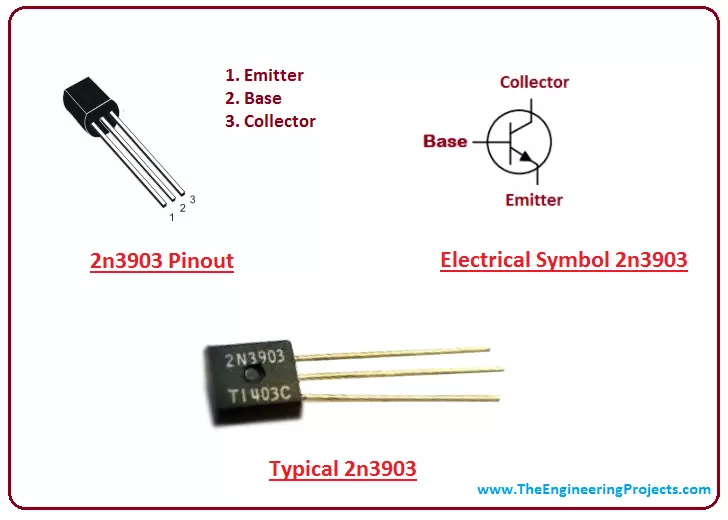
Hi Friends! Hope you are doing great. I am back to give you a daily dose of valuable information so you can excel and grow in your relevant field. Transistors are the fundamental parts of most of the electronic circuits. Today, I am going to unlock the details on the Introduction to 2n3903. It is an NPN transistor main used for general purpose amplification and switching applications. Transistor comes in two types i.e. NPN and PNP transistors. This transistor falls under the category of NPN transistor. This is a bipolar junctions transistor where conduction is carried out by movement of both charge carriers i.e. electrons and holes. However, electrons are major charge carriers in case of NPN transistors. If you are unsure how these bipolar transistors work, you can check this read on Introduction to Bipolar Junction Transistor. I'll reveal each and everything related to this transistor, so you don't get overwhelmed by all data across the web and find all information in one place. Before we move on to the details of this NPN transistor, you must be clear what is transistor? The transistor is an electronic component that comes with three terminals that are used for external connection with the electronic circuits. The voltage applied to one pair of its terminals is used to control the current at the other pair of terminals. Let's dive in and explore what is this about, its pinout, circuit diagram, applications and everything you need to know.

Introduction to 2n3903

  • The 2n3903 is an electronic component called NPN transistor mainly used for general purpose amplification and switching applications.
  • It comes with three terminals called emitter, base, and collector.
  • This transistor has three layers i.e. two N-doped layers and one P-doped layer. The P-doped layer is a semiconductor that is housed between two N-doped layers.
  • The P-doped layer represents the base of the transistor while other two layers represent emitter and collector respectively.
  • All three terminals are different in terms of their size and doping concentration. The emitter is highly doped as compared to base and collector.
  • The base is lightly doped which is responsible for the electron reaction when a voltage is applied at this terminal. When a voltage is applied, it draws small current which is then used to control large current at the emitter and collector terminals.
  • Under normal conditions, the number of electrons diffused into the base terminal is more than the number of holes diffused into the emitter terminal. Electrons act as a majority charge carriers in case of NPN transistor.
  • This transistor is an ideal choice for amplification and switching purpose requiring collector current around 100mA.
Pinout of 2n3903
Following figure shows the pinout of this NPN transistor which is composed of three terminals. 1. Emitter  2. Base 3. Collector 
  • Movement of electrons plays an important role in the current flowing from emitter to collector.
  • The output current obtained at the output terminals is highly dependent on the voltage applied to the base terminal.
  • This bipolar transistor is a current controlled device where small current at the base terminal is used to control large current at other terminals. It is different than MOSFET that is voltage controlled unipolar device where conduction is carried out by one charge carrier i.e either electron or hole.
Circuit Diagram of 2n3903
  • Following figure shows the circuit diagram of this NPN transistor.
  • The emitter is highly doped so it exhibits more current as compared to other terminals. Actually, current at the emitter terminal is a sum of the current at the base and collector terminal.
  • Common-Emitter current gain plays an important role in the amplification process. It is a ratio between collector current and base current. It is called beta and denoted by ß. This is also called amplification factor which defines the amount of current being amplified.
  • Common-Base current gain is another important factor which exhibits lower value than beta. It is a ratio between collector current and emitter current. It is called alpha and denoted by a. Alpha value ranges between 0.95 to 0.99 and most of the time its value is taken as unity.
Absolute Maximum Ratings of 2n3903
  • Following figure shows the absolute maximum ratings of this NPN transistor.
  • These are the stress ratings which play an important role in the execution of the electronic circuit. If these stress ratings are exceeded from absolute maximum ratings, they can damage the device at large, ultimately affecting the overall nature and performance of the project.
  • Similarly, if these ratings are applied for the maximum period of time above normal operating conditions they can affect the reliability of the device.
  • It is advised to check these ratings before placing the device in the circuit and make sure device undergoes and follows same operating conditions and stress ratings as defined by the manufacturer.
  • Steps and measurements taken in the early stages of your project can save you bunch of time and worry and prevents electronic circuit from being affected.
Difference between PNP and NPN Transistors
  • NPN and PNP work in a similar way with the intention of amplification and switching purpose but there is some difference between them.
  • Voltage polarities and direction of currents are opposite in these transistors.
  • Electrons are majority charge carriers in case of NPN transistors while holes are majority charge carriers in case of PNP transistors, however, both types of transistors require both charge carriers for complete conduction process.
  • The base is negative in case of PNP transistor and a negative voltage is applied at the base terminal in order to trigger the holes reaction. And the base is more negative as compared to emitter and collector.
  • While in case of NPN transistor, a base is positive and positive voltage is applied at this terminal in order to trigger electron reaction which draws small current that is used to control large current at the emitter and collector terminals.
  • These transistors are nothing but a combination of diodes joining back to back.
Applications
  • This transistor is mainly used for amplification and switching purpose where collector current around 100mA is required.
You must have look at following articles that are bipolar junctions transistors used for amplification, switching or other electronic applications. 2n5551 - NPN transistor 2n2219 - NPN transistor That's all for today. I hope you have found this article useful. However, if you are unsure or have any question relating to this transistor, you can approach me in the comment section below. I'd love to help you according to best of my expertise and knowledge. Thanks for reading the article.

Introduction to PNP Transistor

Hey Friends! Hope you are doing great. I am back to give you a daily dose of valuable information so you can always stay ahead of your competitors. I have previously updated the article on NPN transistor that is used for amplification and switching purpose. Today, I am going to unveil the details on the Introduction to PNP Transistor which falls under the category of bipolar junction transistors and comes with three layers i.e. two P-doped layers and one N-doped layer where an N-doped layer exists between two P-doped layers. Main Function: Small current at one terminal is used to control large current at other terminals. Major Charge Carriers:  Holes  These NPN and PNP transistors come with their own benefits based on the nature of the electronic project, however, NPN transistors always deems preferable over PNP transistors because of its quick response due to mobility of electrons while PNP transistors are not preferable for amplification and switching purpose because conduction through mobility of holes deems less useful and beneficial as compared to mobility of electrons. In this tutorial, I’ll discuss each and everything related to this PNP transistor i.e what it does, circuit diagram, applications and everything you need to know. Let’s dive in and explore what is this about and how it is used for the execution of electronic projects.

Introduction to PNP Transistor

  • The PNP transistor is a type of bipolar transistor used for amplification and switching purpose and for the designing of the complementary output stage in combination with NPN transistor.
  • It comes with three terminals called emitter, base, and collector where small current at the base terminal is used to control large current at other terminals.
  • It is a current controlled device also known as sinking device where it sinks current into its base terminal and current flows out of the collector.
  • Unlike NPN transistor, current flows from the emitter to collector in this PNP transistor and holes act as a majority charge carriers.
  • This transistor comes with same characteristics as NPN transistor but there are some exceptions. In case of PNP transistor, all voltage polarities and current directions will be reversed as compared to NPN transistor. The PNP transistor sinks current into its base while NPN transistor sources current through its base terminal.
  • Both NPN and PNP transistors are current controlled devices where conduction is carried out by both charge carriers i.e. electrons and holes, but major charge carriers are electrons in case of NPN transistors. While in case of PNP transistor major charge carriers are holes.
  • The PNP transistor is like a combination of diodes combined back to back from cathode sides.
Construction
  • This PNP transistor is composed of two P-doped layers and one N-doped layer where N-doped layer represents the base of the transistor while other P doped layers represent emitter and collector respectively.
  • The base of the transistor is more negative than the emitter terminal.
  • All three terminals in the PNP transistor are different in terms of doping concentration and size.
  • An emitter is highly doped and exhibits 100% current of the transistor while a base is lightly doped which is responsible for the transistor action and controls the number of holes in case of PNP transistor.
  • While collector is lightly doped and comes in a bigger size as compared to other two terminals and collects the number of holes.
Circuit Diagram
  • Following figure shows the circuit diagram of PNP transistor.
  • In PNP transistor, a source voltage is applied at the emitter terminal (instead of collector terminal in case of NPN transistor) and load resistor is applied that is used to resist the current in the collector terminal.
  • Similarly, a bias voltage is applied at the base terminals and a base resistor is connected to this terminal in order to limit the current flowing through this terminal.
  • The emitter is connected to a positive voltage while the base is connected to the negative voltage.
Working
  • Similar to NPN transistor, PNP transistor comes with two pn junctions i.e. emitter-base junction and collector-base junction.
  • An emitter-base junction is forward biased and shows low resistance while collector-base junction is reverse biased and exhibits high resistance. Steps and process required to make these junctions forward biased and reverse biased are different than NPN transistors.
  • Emitter-base junction will become forward biased when a base is negative with respect to the emitter and the voltage at the base side is 0.7 V less than the voltage at the emitter side.
  • Similarly, emitter-base junction is made reverse biased when applied collector voltage is negative. In case of PNP transistor, emitter voltage is much larger than collector voltage.
  • In order to conduct for PNP transistor, emitter voltage must be more positive as compared to both base and collector.
  • The transistor will turn on when there is small current flowing from emitter to base terminal.
  • In PNP transistors emitter emits holes as compared to NPN where emitter emits electrons.
  • When a proper bias voltage is applied at the base terminal, it gets biased and the holes present at emitter terminal moves to the base terminal where they combine with the electron present at this terminal. This generates the small current at the base terminal.
  • The base is very thin so it is very difficult for a base to accept all holes injected by the emitter, as a result, most of the holes leave the base terminal and enter collector terminal.
Matched Switch
  • Combination of PNP transistor with NPN transistor is used for designing and development of the power amplifier circuits. Power B amplifiers are the great example of this amplifier circuits where both PNP and NPN transistors are incorporated together to generate high amplification cycle.
  • Pair of NPN and PNP transistor used in Class B amplifiers is called complementary or matched switch where PNP transistor conducts for the negative half cycle while NPN transistor conducts for the positive half cycle of the transistor.
  • This process is used to generate required power for the loudspeaker in both directions. The resulting power generates at the output current is very high which is then equally shared between matched switch composed of NPN and PNP transistor.
Output Characteristics Curve
  • The output characteristic curve of PNP transistor looks identical to that of NPN transistor but there is one exception i.e. it is rotated by 180 degrees.
  • The same load line is drawn on the characteristic curve that we drew in case of NPN transistor that mentions the operating points of the transistor.
  • The following figure shows the characteristics curve of PNP transistor which is drawn between the output current and collector-emitter voltage and is rotated by 180 degrees where current directions and voltage polarities are reversed. The supply voltage becomes negative for PNP transistor.
  • The current gains (alpha, beta) value are much less in PNP transistor as compared to NPN transistor. We can calculate the beta value from the following equation;
Difference between PNP and NPN Transistors
  • The PNP transistor is known as sinking device while NPN transistor is known as sourcing device.
  • The main difference between PNP and NPN transistor is the proper biasing of the base terminal where current directions and voltage polarities are always opposite to each other.
  • In PNP transistor, holes are majority carriers while in NPN transistor electrons are majority carriers.
  • The emitter voltage is made more positive as compared to both base and collector in PNP transistor. While collector voltage is made more positive as compared to base and emitter in case of NPN transistor.
  • The PNP transistor will be considered ON when there is no current at the base terminal. The NPN transistor will be considered ON when there is enough current present at the base terminal.
  • In PNP transistor current flows from the emitter to collector, while in case of NPN transistor current flows from collector to emitter.
  • The base is positive in case of NPN transistor while it is negative in PNP transistor.
  • When there is enough voltage applied at the base terminal it gets biased in case of NPN terminal while in case of PNP transistor, negative voltage 0.7 V less than emitter voltage must be applied to trigger transistor action.
Applications
  • This transistor is used as a switch for electronic signals.
  • It is used in amplifying circuits.
  • Used as a matched switch in combination with NPN transistor for generating continuous power.
  • Current flow involving heavy motors makes use of these transistors.
  • Used in robotic applications where current sinking is required.
That's all for today. I hope you have found this article useful. If you are unsure or have any question, you can ask me in the comment section below. I'd love to help you in any way I can. You are most welcome to add anything valuable related to this transistor. Thanks for reading the article.

Introduction to NPN Transistor

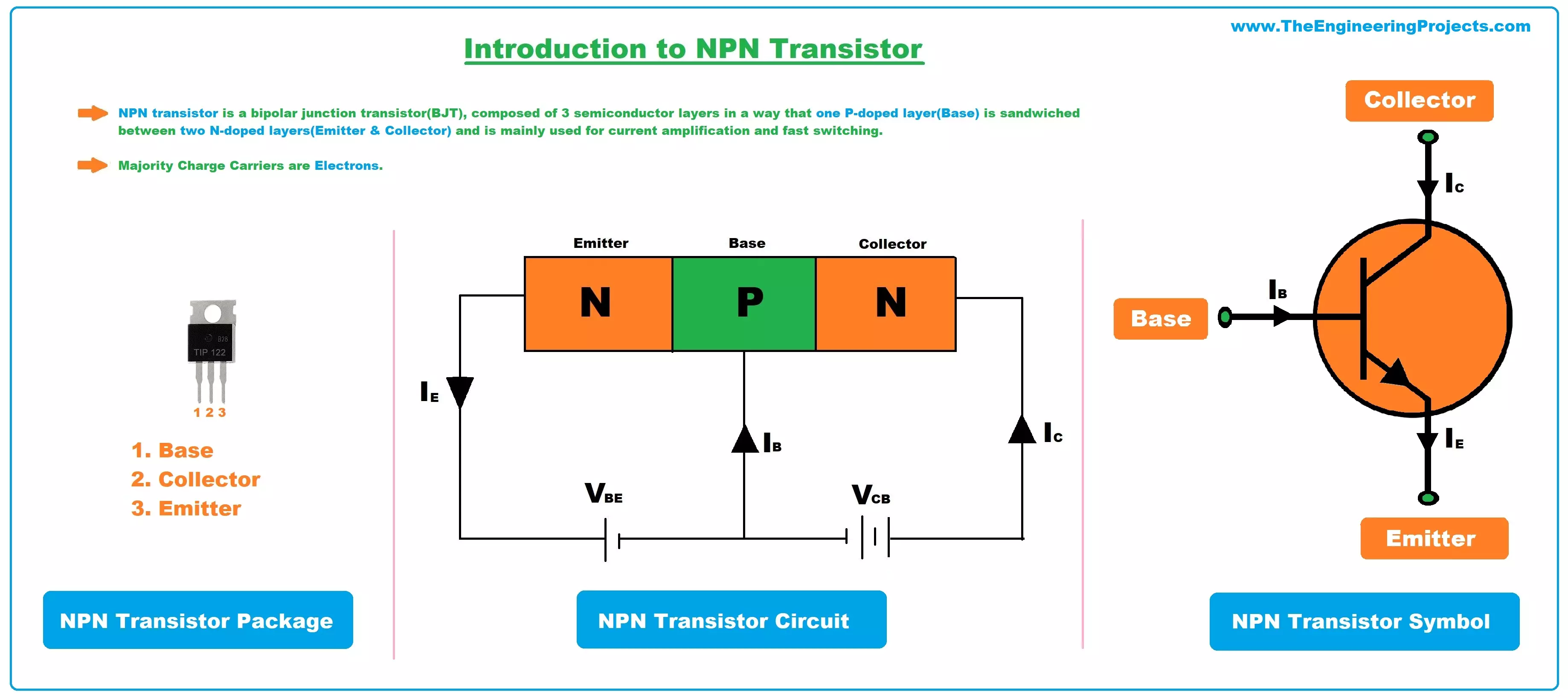
Hello Friends! I hope you are well. Today, I am going to give you a detailed Introduction to NPN transistor. In this tutorial, we'll look at the NPN transistor, how it works, circuit diagram, output characteristics curve, and applications. It is a bipolar junction transistor mainly used for current amplification and switching purposes. BJTs (Bipolar Junction Transistor) are divided into two types i.e. NPN transistor and PNP transistor. Both transistors are different in terms of their electrical composition and construction, however, both are used for amplification and switching purposes in one way or the other.

What is NPN Transistor?

  • NPN transistor is a bipolar junction transistor(BJT), composed of 3 semiconductor layers in a way that one P-doped layer(Base) is sandwiched between two N-doped layers(Emitter & Collector) and is mainly used for current amplification and fast switching.
  • In NPN transistors, the majority charge carriers are electrons and thus conduction is carried out by the flow of electrons from emitter to collector.
  • NPN transistor package comes with three terminals named:
    1. Emitter.
    2. Base.
    3. Collector.
  • These terminals are used for external connection with the circuit and a small current at the base terminal is used to control the large current at the collector and emitter side. (We will cover it in detail in the working section)
Let's have a look at the symbol of NPN transistor:

NPN Transistor Symbol

  • As we use logos to represent companies, similarly in electronics, specific symbols are used to represent components. These electronic symbols prove helpful in designing circuit diagrams especially block diagrams of electronic models.
  • Below figure shows the NPN transistor's Symbol:
Now let's have a look at the Construction of NPN Transistor:

Construction of NPN Transistor

  • NPN transistor consists of 3 regions, two of them are constructed using N-type semiconductor material while the third one is of P-Type Semiconductor.
  • The P-type region is sandwiched between these two N-Type regions.
  • So hypothetically, NPN Transistor is constructed by connecting two diodes in opposite directions.
  • The equivalent circuit of NPN transistor is shown in the below figure:
  • An NPN transistor has two P-N junctions in it, named as:
    1. Emitter-Base Junction.
    2. Collector Base Junction.

Doping Concentration in NPN Transistor

  • Impurities are added to Intrinsic(Pure) Semiconductors which increase their conductivity and are called Extrinsic(Doped) Semiconductors.
  • In NPN transistors, the Base region is heavily doped, the Emitter is lightly doped while Collector's doping lies in between the Base & Emitter.
  • So, in terms of doping concentration from high to low, we have the sequence as follow:

Base > Collector > Emitter

  • Moreover, the Base region is constructed using P-type semiconductors, while Emitter & Collector are designed using N-type semiconductors.
Now, let's have a look at the working of NPN transistors:

How NPN Transistor Works?

  • The NPN transistor comes with two junctions, called:
    1. Emitter-Base Junction.
    2. Collector-Base Junction.
  • The NPN transistor sets in operating condition when an emitter-base junction is forward biased and the collector-base junction is reverse biased and enough current is present at the base terminal. In order to make emitter-base junction forward biased, a positive voltage is applied at the base side and a negative voltage is applied at the emitter side.
  • Similarly, in order to make emitter-base junction reverse biased, collector voltage must be kept more positive than base and collector.
Circuit Diagram
Following figure shows the circuit diagram of the NPN transistor.
  • We can see from the diagram, voltage and resistive loads are applied at the terminals of the transistor.
  • A negative voltage is connected to the emitter while a positive voltage is connected to the base terminals.
  • The base is more positive with respect to the emitter.
  • The resistive load is applied at the base terminal which limits the current produced in this terminal.
  • The positive voltage is applied at the collector terminal and load resistance is applied at this terminal that limits the electrons entering at this terminal.
Working
  • The base is responsible for initiating transistor action. When a voltage is applied at the base, it gets biased and draws a small current which is then used to control a large current at the collector and emitter side.
  • The base action is considered as an ON-OFF valve that generates current when a proper bias voltage is applied at this terminal.
  • The small change in the voltage applied at the base terminal shows a large impact on the output terminals. Actually, the base acts as an input and the collector acts as an output in NPN transistor.
  • In case of silicon transistor emitter-base junction draws voltage around 0.7 when there is no voltage at the base terminal, in order to initiate the electron action and put the transistor in running condition, the base voltage must be greater than 0.7 voltage in the case of silicon transistor and 0.3 in case of germanium transistor.
  • In the N-side of the transistor which represents emitter, the electrons act as the majority charge carriers which are then diffused into the base when a suitable voltage is applied at the base terminal. These electrons act as minority charge carriers when they enter the base terminal, where they join with holes present in the base. Not all electrons join with the holes present at the base terminal. Some of them join with the holes, and the resulting electron-hole pair disappears. Most of the electrons leave the base terminal and then enter the collector region where they again act as a majority charge carriers.
  • When a voltage is applied across the base terminal, the base current is given by;
 
  • Collector current is directly related to base current times a constant factor.
  • In order to increase the efficiency of the NPN transistor, the base is made very thin and a collector is made thick for two reasons i.e collector can handle more heat and accept more electrons diffused through the base terminal.
Current Gains and Relation between Them
  • Current gains play an important role in the amplification process. The common emitter current gain is a ratio between collector current and base current. It is called beta and denoted by ß. It is also known as an amplification factor which defines the amount of current being amplified.
  • Beta is a ratio between two currents, so it features no unit. The beta value is always greater than unity and ranges between 20 to 1000 - 20 for high power transistors and 1000 for low power transistors, however, most of the time its value is taken as 50.
  • Similarly, a common base current gain is another important factor which is a ratio between collector current and emitter current. It is called alpha and denoted by a. An alpha value ranges between 0.95 and 0.99, however, most of the time its value is taken as unity.
  • Following figure shows the relation between two current gains.
  • IF alpha = 0.99 then b = 0.99/0.01 = 99.
  • An alpha value cannot exceed from unity, because it is a ratio between collector current and emitter current i.e emitter current always remains greater than collector current because it exhibits 100% current of the transistor and is equal to the sum of collector current and base current.
NPN Transistor Configurations
  • This NPN transistor can be configured into three configurations called common emitter configuration, common collector configuration, and common base configuration.
  • Common emitter configuration is mostly used for amplification purpose where base acts as an input, collector acts as an output while emitter acts as a common terminal between input and output.
  • This common emitter configuration acts always operates in a linear region where small current at the base side is used to control large current at the collector side.
  • The common emitter configuration used in the electronic circuits always produces inverted output that is highly affected by the bias voltage and temperature. This configuration is an ideal choice for ampliation circuits because it comes with high input impedance and low output impedance and produces the exact voltage and power gain required for amplification purpose.
  • During common emitter configuration, transistor always operates between saturation and cut-off region that helps in amplifying the negative and positive cycles of the input signals. If the base terminal is not biased with the proper voltage, only half of the signal would be amplified.
Output Characteristics Curve of NPN Transistor
Following figure shows the output characteristic curve of the NPN bipolar transistor which is plotted between output collector current and the collector-emitter voltage with varying base current.
  • As described earlier, there will be no output collector current if the applied voltage at the base terminal is zero. When proper bias voltage above 0.7 V, is applied at the base terminal, it gets biased and draws current that controls and effects the output collector current.
  • We can see, Vce directly effects the value of output collector current as long as the applied voltage is 1 V. Above that value collector current no longer remains under the influence of Vce value. In that case, the collector current is widely dependent and controlled by the base current. A small change in the base current and bias voltage would produce a large change in the collector current.
  • The load resistor applied at the collector terminal controls the amount of current entering the collector terminals. Keeping in the view of the load resistor and the voltage applied at the collector-emitter terminals, the collector current is given by;
  • Straight load line between point A and B falls under active region when an emitter-base junction is forward biased and the transistor conducts where electrons are majority charge carriers.
  • The Q point in the graph can be defined by the load line which is actually referred as an operating point of the transistor.
  • The output characteristics curve of this NPN transistor is used to describe the collector current when base current and collector voltage is given.
  • In order to conduct, collector voltage needs to be more positive than base and emitter.
  • It is important to note that, when an emitter-base junction is not forward biased, Ic will be zero, no matter how much voltage is applied at the base terminals. When the emitter-base junction is forward biased and voltage is applied at the base terminal, it draws small current which is then used to control large current at other terminals.
Difference between NPN and PNP Transistors
  • Both NPN and PNP transistors are different in terms of electrical construction and layers doping. NPN stands for negative-positive-negative and also known as sourcing device. While PNP stands for positive-negative-positive and also known as sinking device.
  • In NPN transistor base is positive as compared to emitter and collector voltage is more positive as compared to both emitter and base. Similarly, in PNP transistor base is negative as compared to emitter and emitter voltage is much larger than collector voltage.
  • The voltage polarities and current directions are reversed in both transistors.
  • The NPN transistor conducts and initiates transistor action when a positive voltage is applied at the base terminal. The PNP transistor conducts when a negative voltage lower 0.7 V (for silicon) than emitter voltage is applied at the base terminal.
  • The NPN transistor uses electrons as majority charge carriers for the conduction while PNP transistor uses holes as majority charge carriers for conduction process.
  • In NPN transistor current flows from the collector to emitter while in case of PNP transistor current flows from emitter to collector terminal.
  • Both transistors differ in terms of how they are powered on. The NPN transistor powers on when there is enough current present at the base terminal while PNP transistor powers on when there is no current at the base terminal.
Now, let's have a look at the applications of NPN transistor:

Applications of NPN Transistor

NPN Transistor is the most commonly used type of transistor because of its wide range of applications. A few of NPN transistor applications are as follows:
  • As NPN transistors are fast switching devices, thus they are used for switching purposes i.e. Pulse Width Modulation.
  • NPN transistors are also used as automatic switches in electronics products.
  • Because of high current gain, NPN transistors are used for current amplification i.e. small current at input allows heavy current to pass at the output(Ic).
  • In embedded computers(i.e. microcontrollers, microprocessors etc.), thousands of transistors are joined together(in SMD form) performing different functions i.e. switching of pins.

Real-Life Applications of NPN Transistor

  • Used in logarithmic converters and high-frequency applications.
  • Signal processing and radio transmission applications involve NPN transistors.
  • Darlington pair circuits make use of this NPN transistor for amplifying signals.
  • Used in temperature sensor.
  • Push-Pull amplifying circuits, which fall under the category of the classic amplifier circuit, make use of this NPN transistor.
  • In small quantities, transistors are used to make logic circuits and in the circuits where amplification is required.
That's all for today. I hope you have got clear what is NPN transistor and why it is used for. If you are unsure or have any questions, you can approach me in the comment section below, I'd love to help you according to the best of my expertise and knowledge. Feel free to keep us updated with your feedback and suggestions, they help us provide you quality content that aligns with your needs and requirements. Thanks for reading the article.

Introduction to 2n5884

Hey Friends! Hope you are doing great. I am here to provide you the technical knowledge that helps you stay ahead of your competitors. Today, I am going to unlock the details on the Introduction to 2n5884. It is a power PNP bipolar junction transistor mainly used for general purpose amplification and switching purpose. This is a complementary silicon epitaxial-base transistor that can support 25 A and 80 V. I'll discuss each and everything related to this transistor i.e. what it does, its pinout, circuit diagram and main applications. You must have a look at comprehensive read on Introduction to Bipolar Transistor if you are unsure how these bipolar transistors work. Before we dive into the details of this PNP transistor we must be aware what is transistor? The transistor is a semiconductor device that comes with three terminals where a voltage applied to one pair of terminals controls the current on the other pair of terminals. Let's dive in and explore everything you need to know about this PNP transistor.

Introduction to 2n5884

  • The 2n5884 is a power PNP bipolar transistor mainly used for general purpose amplification and switching purpose.
  • It is a silicon semiconductor device that comes with three terminals called emitter, base, and collector.
  • It comes with three layers where one N-doped layer is housed between two P-doped layers. The N layer represents the base of the transistor, while other two layers represent emitter and collector respectively.
  • This component is also known as a current controlled device where a voltage applied at the base terminal is used to control large current at the emitter and collector terminals.
  • This PNP component is a little bit different than its counterpart NPN transistor, however, both are bipolar components where current is carried out by the movement of both charge carriers i.e. electrons and holes. Electrons are major charge carriers in NPN transistor and holes are major charge carriers in PNP transistor.
  • When a voltage is applied at the base terminal, it gets biased and draws current which is then used to control large current at the emitter and collector terminals.
  • All these three terminals are different in terms of their size and doping concentration. An emitter is highly doped and carries more current as compared to base and collector. The base is lightly doped which is responsible to trigger electron reaction at the base terminal. The collector is moderately doped which accepts the holes in case of this PNP transistor.
  • Output current obtained at the collector terminal is highly dependent on the voltage applied at the base terminal. This process is used for amplification purpose.
  • You must have a look at the construction of diode which plays a vital role in the construction of this bipolar transistor.
Pinout of 2n5884
  • Following figure shows the pinout of this PNP transistor which is composed of three terminals.
1. Base 2. Emitter 3. Collector 
  • Movement of holes plays an important role in the output current obtained at the output terminals.
  • Unlike NPN transistor, a negative voltage is applied at the base terminal in this PNP transistor where the base is more negative as compared to emitter and collector.
Circuit Diagram of 2n5884
Following figure shows the circuit diagram of 2n5884.
  • An emitter is highly doped so current at the emitter side more than current at the collector and base side. Actually, emitter current is the sum of base and collector current.
  • Unlike NPN transistor, holes are diffused through the base from the emitter in this PNP transistor, which are then collected by the collector.
  • This PNP transistor is used for amplification purpose, however, most of the professionals don't recommend this transistor for amplification purpose and pick NPN transistor for amplification because conduction carried out by the movement of electrons is more effective and suitable than conduction carried out by the movement of holes.
  • This transistor is different than JFET which is unipolar transistor i.e conduction is carried out by single charge carrier.
Absolute Maximum Ratings
  • Following figure shows the absolute maximum ratings of this PNP transistor.
  • It is important to note that, these are the suitable stress ratings recommended by the manufacturer, which if exceed from absolute maximum ratings, can damage the device severely.
  • Similarly, if these ratings are applied for the maximum period of time above normal operating conditions, they can affect the overall reliability of the device.
  • Take these ratings into consideration and make sure this component exhibits and follows same ratings defined by the manufacturer before you intend to place this component into your project.
  • Proper measurements taken the early stages of your project can save your bunch of time and worry that can affect the nature and overall performance of the project.
Applications
  • This component is used for amplification and switching purpose.
You must also have a look at following transistors of same nature used for amplification, switching, and different electronic applications. That's all for today. I hope you have found enough information about this component. In case you are feeling unsure or have any question, you can ask me in the comment section below. I'd love to help you according to best of my knowledge and expertise. Keep your suggestions and feedback coming, they allow us to give you quality content that aligns with your field of interest. Thanks for reading the article.

Introduction to 7805

Hey Fellas! We always strive to keep you updated with best and valuable information so you keep coming back for what we have to offer. Today, I am going to uncover the details on the Introduction to 7805. It is a positive voltage regulator used for providing constant output voltage over a wide range of input voltage. Before we move on, you must be clear what is voltage regulation? Voltage regulation is referred as the measure of voltage change between input and output. The IC 7805 does the same thing. It provides constant output voltage when a range of different voltage is applied at the input terminal. This component comes with three terminals called input, ground, and output. This is called positive voltage regulator because it generates positive voltage with respect to the ground terminal. Transistors and voltage regulator IC like 7805 work in a similar way with the intention of providing voltage regulation. I'll discuss each and everything related this integrated circuits, so you get a clear idea what it does, and how it is used over a wide range of applications. Let's dive in and explore what is this about and everything you need to know.

Introduction to 7805

  • 7805 is an IC used for voltage regulation and comes in TO-220 version. This component belongs to 78xx series where xx defines the output voltage it generates.
  • Voltage fluctuation is a common practice during the execution of many electronic projects. This component overcomes and prevents this voltage fluctuation by providing a constant output voltage at the output terminal.
  • The best part is that it doesn't require any additional components to set output voltage.
  • It is a compact IC that comes with a built-in protection circuit that avoids the circuits from too much heating, making it suitable for circuits drawing high current.
  • The input voltage range applied to the input terminals of this IC varies from 7 V to 18 V (in some cases 7 to 35 V), resulting in the generation of constant output voltage around 5 V.
  • You can see, there is a huge difference between input voltage and the output voltage that gets regulated. This difference is discharged as heat. The surge of heat generation can damage the device and affect the overall project performance.
  • There are two ways to overcome this heat generation i.e. you can use a heat sink that is widely used for heat dissipation OR you can limit the input current 2 to 3 V above the regulated voltage at the output terminal. For example, you'll get 5 V at the output terminal, so it is suitable to limit input voltage within 7 or 8 V.
  • Heat sink comes in different sizes based on the amount of heat that is required to disperse. It is advised to calculate the size of heat sink before you put your voltage regulator in operation.
  • With the addition of heat sink, this IC can control output current at around 1.0 A.
  • This voltage regulator is an ideal choice for the applications where safe area compensation, thermal shutdown, and current limiting is required.
  • This device is designed with the purpose of getting constant output voltage, however, it can be coupled with external components with the intention of generating desired voltage and current.
  • This IC comes with an accurate circuit which generates constant voltage so no capacitors are required to produce smooth output, however, it is advised to place 10µF capacitors in the input and output terminal to remain in the safer side.
Pinout of 7805
  • Following figure shows the pinout of this voltage regulator.
  • Pin 1 shows the input voltage applied to this regulator which ranges between 7 to 18 V.
  • Pin 2 shows the ground terminal. Voltage regulator generates positive voltage with respect to the ground terminal.
  • Pin 3 shows the output terminal where regulated voltage is obtained. Regulated voltage shows the tolerance between 1.5 % to 2 %.
  • This regulator has a capacity of controlling output current around 1 A.
  • It shows a voltage dropout around 2 V. It is advised to provide minimum 7 V at the input terminal in order to obtain exact 5 V at the output terminal.
Absolute Maximum Ratings
  • Following figure shows the absolute maximum ratings of 7805.
  • These are the stress ratings, which if exceed from absolute maximum ratings, can damage the device severely.
  • Before you place this regulator in the circuit, make sure it undergoes and exhibits same stress ratings as defined by the manufacturer.
  • Similarly, it these stress ratings are applied for a maximum period of time above the normal operating conditions, they can affect the device reliability.
  • These ratings are obtained with a storage temperature range at around 150 °C.
  • This IC exhibits a thermal resistance around 5 °C/W which is the resistance in the heat flow.
Applications
This voltage regulator is used over a wide range of applications. Following are some main applications of this regulator.
  • Used in a circuit where a constant voltage is required.
  • It is used in a phone charger and portable CD player.
  • UPS power supply circuit and remote control extension make use of this regulator.
  • This regulator is widely used where internal circuit current limiting is required.
  • Safe area compensation is another advantage obtained from this regulator.
  • This regulator is mainly used for generating constant voltage output, but it can be customized to use for the required current and voltage at the output.
  • It is an ideal choice for the applications which support current around 1.0 A to 1.5 A which cannot be obtained without proper heat sinking.
  • Safe operating area protection and thermal shutdown make it suitable for many applications involving high temperature and pressure.
That's all for today. I hope you have found this article useful. If you are unsure or have any question, you can ask me in the comment section below. I'd love to help you according to best of my expertise in any way I can. Keep your feedback and suggestions coming. They allow us to provide you quality work that aligns with your needs and demands. Thanks for reading the article.

Introduction to 2n3792

Hey Guys! Hope you are doing great. Transistors are the fundamental parts of the recent electronic devices. They are available in two types i.e. NPN and PNP transistors. Based on the technical aspect and utilization, both types come with different benefits and advantages. Today, I am going to discuss the details on the Introduction to 2n3792. It is a PNP (positive-negative-positive) silicon bipolar power transistor mainly used for amplification and medium speed switching. It is manufactured using epitaxial planer process and comes in TO-3 casing. I'll cover each and everything related to this transistor so you don't need to go anywhere and find all information in one place. Let's explore what is this about, its main applications and everything you need to know.

Introduction to 2n3792

  • The 2n3792 is a PNP bipolar transistor which is mainly used for amplification and medium speed switching applications.
  • It consists of three layers where one N-doped layer is housed between two P-doped layers.
  • It has three terminals called emitter, base, and collector. All these terminals are different in terms of their doping concentrations. The emitter is highly doped as compared to base and collector terminals.
  • In this transistor, base-emitter is more positive with respect to base and collector. While negative biased voltage is applied at the base terminal.
  • It is a current controlled device where small current at the base side is used to control the large current at other terminals.
  • In this PNP transistor, current directions and voltage polarities will be reversed as compared to NPN transistors.
  • It works in a similar way to NPN transistor i.e. both are used for amplification purpose where small current at the base side is used to control the large current at the emitter and collector side, however, there is one exception, unlike NPN transistor, holes are diffused through base from the emitter and collected by the collector.
  • This PNP transistor is rarely used for amplification purpose because conduction carried out by the movement of electrons is considered more valuable than conduction carried out by the movement of holes.
Pinout of 2n3792
  • Following figure shows the pinout of this PNP transistor. It consists of three terminals.
1. Base 2. Emitter 3. Collector 
  • Voltage is applied at the base terminal, which draws small current.
  • The output current obtained at the collector terminal is highly dependent on the voltage applied at the base terminal. This process is used for amplification purpose.
Circuits Diagram of 2n3792
  • Following figure shows the circuit diagram of 2n3792.
  • Current at the emitter terminal is equal to the sum of current at the base and collector side. The emitter is highly doped so it exhibits more current as compared to other terminals.
  • In this transistor current direction is reversed as compared to NPN transistor. In this case, current flows from collector to emitter.
  • Voltage polarities are also reversed. Negatively biased voltage is applied at the base terminal in order to initiate holes reaction which is then used to control the large current at the other terminals.
  • As the name suggests, this is a bipolar junction transistor where conduction is carried out by both charge carriers i.e. electrons and holes, but holes are majority charge carriers in this case. While electrons are majority charge carriers in NPN transistors.
Absolute Maximum Ratings of the 2n3792
  • Following figure shows the absolute maximum rating of the 2n3792.
  • These are the stress ratings that play an important role in the selection of this transistor for electronic circuits.
  • If stress ratings exceed the absolute maximum ratings, they can damage the device.
  • Similarly, if these ratings are applied for the maximum period of time above normal operating conditions, they can effect the reliability of the transistor. Before you pick this transistor for your project, make sure, it exhibits and undergoes same ratings as defined by the manufacturer.
  • Power dissipation is 150 W and these absolute maximum ratings are taken at the absolute junction temperature around 200 ºC.
  • Thermal resistance is 1.17 ºC/W which is the measure of resistance to the heat flow.
Applications
  • This transistor is used for medium speed switching applications.
  • It is also used for an amplification purpose.
That’s all for today. I hope you have found this article useful. If you are unsure or have any question, you can ask me in the comment section below. Your suggestions and feedback will be highly appreciated, they allow us to provide you quality work that resonates with your needs and expectations. Thanks for reading the article.

Introduction to 2n4123

Hey Guys! I am back to give you a daily dose of information so you can excel and grow in your relevant field and keep coming back for what we have to offer. If you are a hobbyist or student, you require a transistor for the execution of your project every now and then. Today, I am going to unlock the details on the Introduction to 2n4123. It is an NPN (negative-positive-negative) general purpose transistor which is mainly used for the amplification and switching purpose where collector current around 100mA is required. It is a semiconductor device mainly composed of silicon and comes with three terminals where a voltage applied to the one pair of terminals is used to control the current at the other pair of terminals. I'll break down each and everything related to this transistor in easy steps so you can grab the main concept easily. Let's dive in.

Introduction to 2n4123

  • The 2n4123 is an NPN bipolar junction transistor mainly used for amplification and switching purpose, especially where collector current of 100mA is required.
  • This transistor comes with three terminals called emitter, base, and collector that are used for the external connection with the electronic circuits.
  • All these three terminals are different in terms of doping concentration. Emitter terminal is highly doped as compared to base and collector terminals.
  • The base terminal is lightly doped which controls the number of electrons. Collector terminal is moderately doped which collects the number of electrons from the base terminal.
  • Actually, NPN transistor is a combination of diodes joining back to back.
  • This NPN transistor is termed as a current controlled device which is different than JFET that is voltage controlled device.
  • One P-doped semiconductor layer is housed between the other two N-doped layers. The P-doped layer represents the base terminal while other two layers represent emitter and collector respectively.
  • When a voltage is applied at the base terminal, it draws small current which is then used to control large current at the emitter and collector terminals.
  • This process is used for amplification purpose where small current controls the large current.
  • An output current obtained at the collector terminal is highly dependent on the intensity of voltage applied at the base terminal.
  • This transistor operates in forward biased mode. If a transistor is not forward biased, collector current will be zero, no matter how much voltage is applied at the base terminal.
2n4123 Pinout
Following figure shows the pinout of this NPN transistor which mainly consists of three terminals. 1. Emitter 2. Base 3. Collector 
  • When a voltage is applied at the base terminal, it triggers the electron reaction, resulting in the diffusion of electrons from the base to collector terminal.
  • This movement of electrons is highly dependent on the voltage applied at the base terminal.
  • The number of electrons diffused into the base terminal from the emitter is greater than the number of holes diffused into the emitter region.
  • When the electron enters the base terminal it combines with the hole inside the base terminal where resulting pair disappears.
  • The base terminal cannot control all electrons diffused into it from the emitter terminal, resulting in the transfer of electrons from the base to collector terminal.
Circuit Diagram of 2n4123
  • Following figure shows the circuit diagram of the 2n4123.
  • Current at the emitter terminal is equal to the sum of base and collector current because doping concentration of emitter is more than other terminals.
  • The base is more positive with respect to the emitter which makes it an ideal choice for controlling the number of electrons.
  • There are two current gain factors that are mostly used to determine the characteristics of the transistor. One is common-emitter current gain which is a ratio between collector current and base current. This is called Beta and denoted by ß.
  • Its value ranges between 20 to 1000, however, the standard value is taken as 200.
  • Beta is a ratio between two currents so it exhibits no unit. It is also known as amplification factor and determines the amount of current being amplified.
  • Another current gain is common-base current gain which is a ratio between collector current and emitter current. It is called alpha and denoted by a. Alpha value ranges between 0.95 to 0.99, however, most of the time its value is taken as unity.
  • It is important to note that if we interchange emitter and collector, then the transistor will become reverse biased and these current gains show low value as compared to values taken from forward biased transistor.
  • In this NPN transistor, electrons are main charge carriers, which is different than PNP transistor where holes are major charge carriers.
Absolute Maximum Ratings of 2n4123
  • Following figure shows the absolute maximum ratings of this transistor.
  • These are the stress ratings that must be controlled before you place this component in the electronic circuit.
  • If these stress ratings are exceeded from the absolute maximum ratings, they can damage the device at large, which ultimately affect the performance of the project.
  • Similarly, if these stress ratings are applied for a maximum period of time above normal operating conditions, they can affect the device reliability.
  • These ratings are determined on the basis of the maximum junction temperature of 150 °C.
Applications
  • This NPN transistor is mainly used for general purpose amplification.
  • Switching applications involve this NPN transistor where collector current around 100mA is required.
That's all for today. I hope you have found this article useful. If you are unsure or have any question, you can ask me in the comment section below. I'd love to help you in any way I can. Keep your suggestions coming. Your valuable suggestions and feedback keep us busy providing you quality work that resonates with your field of interest. Thanks for reading the article.

Magnetic Reed Switch Library for Proteus

Hello friends, I hope you all are doing great. In today's tutorial, I am going to share new Magnetic Reed Switch Library for Proteus. We are quite proud to share it as its not been designed before. Our TEP Team has designed it and I think they need a little appreciation. :P You can interface it with any Microcontroller like Arduino, PIC or 8051 Microcontroller etc. As Proteus is a simulation software so we can't produce magnetic field in it. That's why, we have placed a TestPin and when you provide HIGH Signal to that TestPin then it will act as it has magnet around. Similarly, if you provide LOW Signal to that TestPin then it will behave normal and will sense no magnet around. Rite now, we have just designed two Magnetic Reed Switches but soon we will design other Reed Switches as well. So, let's get started with How to download and use Magnetic Reed Switch Library for Proteus.

Magnetic Reed Switch Library for Proteus

  • First of all, download this Magnetic Reed Switch Library for Proteus by clicking the below button:
Download Proteus Library Files
  • You will get a .rar file so unzip it using winrar.
  • Inside this .rar file, you will find three Proteus Library files, named as:
    • MagneticReedSwitchesLibraryTEP.IDX
    • MagneticReedSwitchesLibraryTEP.DLL
    • MagneticReedSwitchesLibraryTEP.HEX
  • Place all these three files in the Library folder of your Proteus 7 or 8 Professional.
Note:
  • Here are the images of these real Magnetic Reed Switch Modules along with our designed modules in Proteus:
  • We have designed these two modules, both of these modules give digital output only in Proteus but in real the reed module with red color also gives analog output.
  • We are not yet able to produce analog output in Proteus, so that's why we have only digital output. :)
  • Now I hope that you have placed all those three Proteus Library files in the Library folder of your Proteus software, so open your Proteus software or restart it.
  • In Proteus software, go to your components search box and make a search for Magnetic Reed Switch as shown in below figure:
  • Now place both of these modules in your Proteus software and they will look something, as shown in below figure:
  • Double click any of these modules and its Properties panel will open up.
  • Now in the Program File section, browse to our downloaded Library file MagneticReedSwitchesLibraryTEP.HEX as shown in below figure:
  • Now click OK to close this Properties window.
  • You can see we have four pins in total attached to our Magnetic Reed Switch, which are:
    • Vcc: We have to provide +5V at this pin.
    • GND: We have to provide Ground (0V) at this pin.
    • D0: That's the Output Pin, it will be HIGH when some magnet is around otherwise remain LOW.
    • TestPin: As Proteus a simulation so we can't provide magnetic field, that's why we have palced this TestPin. If TestPin is HIGH then it means magnetic field is around and if its LOW then there's no magnet around.
  • I hope you have understood the pinout of this Reed Switch, so now let's design a simple simulation to test them out.
  • So, design a simple circuit in Proteus as shown in below figure:
  • Now run your simulation, and change the Logic State from 0 to 1, which is connected at TestPin.
  • If everything goes fine then you will get such results:
  • As you can see in the above figure that D0 Pin is HIGH when I changed the Logic State from 0 to 1 and that's why LED attached at D0 Pin is now ON.
  • I have also designed a similar simulation for the other Magnetic Reed Switch and its ON state is shown in below figure:
  • I have already added both of these simulations in the above download file.
  • So, first add your Library and then run these simulations.
  • I will soon interface this sensor with different Microcontrollers like Arduino, 8051 Microcontroller, PIC Microcontroller etc.
So, that's was all for today. I hope you will enjoy this Magnetic Reed Switch Library for Proteus and will use it in your Engineering Projects. Thanks for reading & have fun !!! :)

Diode: Definition, Symbol, Working, Characteristics, Types & Applications

Hi Guys! Hope you are doing great. Today, we will have a look at an electronic component named Diode. We will discuss Diode working, Symbol, Applications and characteristics in detail.

A diode is an electronic component, that allows the flow of current in one direction only. It exhibits low resistance in one direction and very high resistance in the opposite direction. Whoever has been a science student, knows about diodes. Although it seems to be a tiny component of a circuit, apparently it is true but it has a lot of complexities or you can say, it's a storm in a teacup.

Diodes are normally used in rectifiers, where they convert AC signals to DC signals. They come with a wide range of applications including power conversion, radio modulation, logic gates, temperature measurements and current steering. I'll try to cover everything related to diodes so let's get started:

Diode Definition

  • A diode is a 2-terminal, basic discreet electronic component, made up of semiconductor material, which allows a unidirectional flow of current through it, i.e it only conducts current in one direction.
  • A diode is analogous to a uni-directional water flow valve, which allows the water to flow in one direction but restricts it to flow backward.
  • Diode consists of two terminals, named:
    • Anode (+).
    • Cathode (-).
  • These terminals are connected to two doping regions:
    • P-Type region.
    • N-Type region.
  • The P-Type region consists of positively charged ions called Holes, while the N-Type region consists of negatively charged electrons. We will discuss its construction in detail later.
  • In a diode, current flows from Anode to Cathode(diode acts as a closed switch), but if the current flows in the opposite direction(i.e. from Cathode to Anode), the diode will block it, so we can say, the diode is acting as an open switch.

Diode Symbol

  • The diode symbol and its real package are shown in the below figure:
  • The arrowhead in a diode symbol represents the direction of the current flow i.e. current can flow from anode to cathode.

Construction of Diode

Now let's have a look at the construction of a diode:
  • A diode is normally made up of a semiconductor material i.e. silicon, germanium, gallium arsenide etc.
  • Two crystals of the same semiconductor material(normally silicon) are doped with different types of impurities, one crystal with pentavalent impurity, while the second one with trivalent, to create two types of semiconductor materials named:
    • P-Type Semiconductor: Majority Charge Carriers are Holes(+).
    • N-Type Semiconductor: Majority Charge Carriers are Electrons(-).
  • When these two semiconductors are joined/merged together, the free electrons from the N-Type start to move towards the P-Type region, while the Holes start moving towards the N-Type region.
  • At the border of these two regions, electrons get combined with Holes and neutralized.
  • These neutralized atoms create a layer at the border(of N-Type & P-Type regions) and stop the flow of electrons & Holes. This newly created third layer/region is called the depletion region.
  • The depletion region is very small in size and acts as a barrier for the flow of charge carriers(i.e. electrons & Holes) from the N-type to P-type region.
  • Below diagram will give you a better idea of Diode construction:
  • As you can see in the above figure, we have 3 regions in a final diode, named:
  1. N-Type Region: Majority Charge Carriers are Electrons(-).
  2. P-Type Region: Majority Charge Carriers are Holes(+).
  3. Depletion Region: No Charge(Neutral)
  • Two electrically conductive electrodes/probes are connected to these two Regions and are called:
    • Cathode: Connected to N-Type Region.
    • Anode: Connected to P-Type Region.
You must have understood by now, how diodes are constructed? Now, let's have a look at How diode works?

Diode Working

As we discussed in the above section, when two semiconductor materials are merged together, a momentary flow of charge carriers occurs, which results in the creation of a depletion region. This state of the diode is normally termed as Zero Biasing State, as there's no power applied at any terminal. In operational mode, the diode has two other biasing states, named as:
  • Forward biased.
  • Reverse biased.

Diode as Forward Biased

  • The PN Junction created at the center of two regions is very small but it's powerful enough to stop the free electrons from passing through it.
  • So, if we could provide some external power to these electrons, they can break this barrier and can make their entry into the P-Type region.
  • This external power required to overcome the depletion region is normally termed as a Forward Threshold Voltage of diode.
  • This threshold voltage value depends on the semiconductor material used in the diode construction i.e. for silicon it's +0.7V and for Germanium, it's +0.3V.
  • So, for a normal diode, if we provide an external power of +0.7V, the electrons will overcome the depletion region and in simple words, the current will start flowing through the diode.
  • As you can see in the below figure, the positive terminal of the battery is connected with the anode of the diode and as we will provide a voltage greater than its threshold voltage, the diode will start conducting and is said to be acting as forward biased.
  • In forward biasing conditions, an ideal diode has zero resistance, but as I told you earlier, an ideal condition does not exist.

Diode as Reverse Biased

  • If the polarity of the applied power is reversed i.e. positive terminal of the battery gets connected with the cathode(-), while the negative terminal gets connected with the anode(+), the depletion region will start to increase.
  • In this state, the diode won't allow the current to flow through it and is said to be acting as reverse biased.
  • In a reverse Biased state, the diode acts as an open switch.
  • The PN junction in reverse biasing offers a very high resistance due to the thickness of the depletion region.
  • A diode in ideal condition when reverse biased has infinite resistance.

History of Diode

  • Introduced in 1906, the first semiconductor diode was named as Cat's Whisker Diode that was fabricated using mineral crystals.
  • Mostly, diodes are designed using silicon because it can handle high temperature, however, germanium is also used when low voltage drop is required.
  • When there is no applied voltage across the diode terminals, the diode will not conduct and very thin depletion region exists with no charge carriers around the pn junction of the diode.
  • The diode will only conduct when applied voltage at the forward biased condition is greater than the diode built-in potential and it allows the flow of electrons from the cathode to the anode.
  • Don't get confused with the arrow sign of the diode pointing from the anode to the cathode. It shows the conventional current flowing from anode to cathode. Conduction will be carried out from cathode to anode when a certain voltage above built-in potential is applied.
 
  • A diode will stop conducting when the applied voltage is reverse biased and allows the depletion region to expand, blocking the flow of current. However, when a reverse biased voltage is too large, it allows the small current to flow which is called leakage current. It is too small that most of the time it is ignored while considering the current ratings.
  • Similarly, when the reverse biased voltage is too large, it allows the depletion region to expand too much till it collapses, reaching a condition called breakdown, which appears to be very harmful for the quality and operation of the device.
  • When we check the value of resistance by multimeter, it shows the low value at one terminal and high value at other terminal which indicates diode is working. It doesn't indicate the actual value of the resistance, instead, it shows the voltage drop across the pn junction.
  • For silicon diodes, the forward voltage drop is 0.7 V, which is the voltage required to overcome built-in voltage in order to start the flow of current from cathode to the anode. Similarly, forward voltage drop for germanium is 0.3 voltage which makes it an ideal choice for the applications where low voltage drop is required.
  • The voltage drop is highly dependent on the current flowing through the diode, however, it remains constant over a wide range of currents.

Junction Diodes

Diodes are divided into two types based on the formation of the junction between the terminals.

p-n junction Diode

  • A pn junction diode is made from semiconductors like silicon or germanium where an N-type region is created with the help of negative charge carriers called n-type semiconductor while the P-type region is created with the addition of positive charge carriers called p-type semiconductors.
  • Initially, there is no flow of current between two regions until they are joined together, resulting in a formation of pn junction where movement of electrons starts from N-type semiconductor to P-type semiconductor.
  • There exists a region around pn junction where there are no charge carriers called depletion region. When depletion is very thin, indicates a conduction from N-type region to P-type region. When deletion region is very large, indicates no or little flow of current between two regions.
  • The diode action takes place around the pn junction. When forward voltage potential more than built-in potential is applied between the diode terminals, it allows the flow of electrons from N-type region to P-type region, while blocking the flow of electrons in reverse order.
  • Foward biased mode means the flow of electrons from N type to P type region. Reverse biased mode means no flow of electrons, blocking the current in other direction.

Schottky Diode

  • Schottky diode is another type of junction diode where the junction is formed using metal-semiconductor instead of using p-n junction. It is an ideal choice for the applications where high switching speed is required.

Current-Voltage Characteristics

The voltage in V-I curve shows the voltage applied across the diode terminals and current shows the corresponding current obtained as the result of the applied voltage. Based on needs and requirements, the V-I characteristics of the diode can be customized using the suitable semiconductor material and doping concentration of impurities during the manufacturing of the device.
  • The depletion region housed between the pn junction shows how the movement of electrons between the two N-type and P-type regions takes place.
  • When pn junction is formed, the electrons from N-type region transfers to the P-type region, where they join the holes present in the P-type region.
  • When electron combines the hole, the resulting pair disappears and the region around pn junction gets depleted with no charge carriers present. Resulting depletion region around the pn junction acts as an insulator.
  • It is important to note, the width of depletion region cannot exceed without limit. When an electron-hole pair is created, it results in the formation of positively charged ion in the N-type region and negatively charged acceptor ion in the P-type region.
  • As the formation of electron-hole pair proceeds, it results in the creation of built-in potential where increasing electric field developed around the depletion region, stops the further formation of an electron-hole pair.

Foward Biased Mode

  • When the external voltage applied between the diode terminals comes with opposite polarity as the built-in potential, it starts the current flow where depletion region acts as a conductor. In this case, the depletion region formed around the pn junction will be very thin.
  • The built-in potential is different for different diodes i.e. 0.7 for silicon and 0.3 for germanium.
  • If the external voltage of opposite polarity with more than 0.7 V is applied between the diode terminals in case of a silicon diode, it allows the current to flow from anode to cathode. The diode is considered as "turned on" in this case.
  • The voltage above which diode starts conducting through depletion region around the pn junction is called forward threshold voltage which is different than the built-in voltage.

Reverse Biased Mode

  • When the external voltage applied between the diode terminals comes with the same polarity as built-in potential, it allows the depletion region to expand and stops the flow of current where depletion region acts as an insulator.

Types of Diodes

There are many types of diodes available in the market which are mainly used for the customization of voltage or current. Most of the pn junction diodes are made from silicon and germanium. Before the inception of these power diodes, selenium was used to manufacture the diodes.

Selenium diodes come with low efficiency as compared to silicon diodes, because high forward voltage around 1.4 or 1.7 V is required to start conducting around the pn junction, resulting in the need of much larger heat sink. Following are the most commonly used diodes in the electronic devices.

LED Diodes

  • These diodes are made from the crystalline substance that emits light in different colors like red blue green or orange, depending on the crystalline material used in the diode.
  • These diodes emit incoherent, narrow-spectrum light, capable of producing wavelengths in the wide range.
  • Most of the LED diodes are low-efficiency diodes, which make them an ideal choice for the signal applications. LED diodes are also used in the formation of opto-isolator.

Avalanche Diodes

  • These diodes are very identical to Zener diodes, where they start conducting in the reverse direction when reverse bias voltage becomes greater than break down voltage. These diodes come with an ability to break down at a certain voltage, without destroying them completely.
  • Both Zener and Avalanche diodes are quite similar with respect to their mode of operation with one practical difference i.e. both didoes exhibit temperature coefficient with opposite polarities.

Zener Diodes

  • Zener diodes, also termed as reverse breakdown diodes, are the diodes that conduct in reverse bias condition.
  • Zener breakdown effect occurs at a very specific voltage, making them suitable for use as a precision reference voltage.
  • In reference circuits, temperature coefficient balancing can be achieved by using a combination of zener diodes and switching diodes.
  • Both avalanche and zener diodes fall under the category of breakdown diodes and electrically they response quite similar with one exception i.e. zener diodes operate with a breakdown voltage below 5 V, while avalanche diodes operate with a breakdown voltage above 5 V.

Crystal Diodes

  • Crystal diode, also known as Cat's Whisker diode, is point contact diode which is not easily available in the market. This diode comes with a thin metal, known as an anode, and semiconductor crystal, known as a cathode.

Photodiodes

  • Photodiodes are composed of semiconductor materials that are light sensitive, making them an ideal choice for solar cells and optical communications.
  • These diodes are mostly available in single diode package, however, single dimensional or double dimensional array combination is also widely available.

Applications

Diodes allow the current to flow in one direction which makes them suitable for most of the applications where current controlling is prerequisite. Following are the major applications of the diodes.

ONE. Logic gates are designed using diodes with other electronic components.

TWO. Diodes are also used as a waveform clipper, where they clip the negative or positive peak of the signal in order to attain specific voltage.

THREE. Didoes are helpful for temperature measuring because the forward voltage drop across them is very sensitive to temperature. Most of the diodes come with negative temperature coefficient which remains constant above 20 Kelvin.

FOUR. Diodes are widely used for the demodulation of amplitude signal. The amplitude of AM signal is directly proportional to the original audio signal and comes with positive and negative peaks of the carrier wave. The diode is used to rectify the AM radio signal, resulting in only positive peaks of the carrier wave. A filter is applied in order to extract the audio signal from radio carrier wave, which then produces sound waves when applied to the amplifier.

FIVE. Rectifiers are made from diodes which widely replace the commutator for converting AC signal to DC signal.

SIX. Some electronic circuits are very sensitive and show high spikes in the voltage during the execution of the project. These diodes are used to prevent the circuits from high voltages spikes which appear to be very damaging, if not controlled properly, in the early stages.

That's all for today. I hope you have found this article useful. If you're unsure or have any question, you can approach me in the comment section below. I'd love to help you according to best of my expertise in any way I can. Feel free to keep us updated with your suggestions, they help us to provide you quality work that resonates with your needs and demands. Thanks for reading the article.

Introduction to 2n6491

Hello Friends! Hope you are doing great. We always come up with useful information that helps you solve your problems and keeps you updated with the knowledge that resonates with your needs and demands. Today, I am going to unlock the details on the Introduction to 2n6491. It is an NPN power transistor mainly used for general purpose amplification and switching purpose. It exhibits high DC current gain and comes with TO-220 package. I'll break down all information related to this transistor in easy steps, so you can grab the main concept easily. Let's dive in and explore what is this about and its main applications.

Introduction to 2n6491

  • 2n6491 is an NPN (negative-positive-negative) bipolar junction transistor mainly used for general purpose amplification and switching purpose.
  • It has three terminals used for external connection with the electronic circuits called emitter, base, and collector.
  • All these three terminals are different in terms of their doping concentration. An emitter is highly doped as compared to base and collector.
  • The base is lightly doped which is responsible to trigger the electron reaction in the transistor.
  • The collector is moderately doped which is used to collect the electors from base terminals.
  • When a voltage is applied at the base terminals, it gets triggered and starts the electron reaction.
  • The base terminal then draws small current which is used to control large current at the collector and emitter side.
  • This transistor is a current controlled device where small current at the base side is used to control the large current at the other terminals.
  • The number of electrons from emitter side is diffused to the base side where they act as minority carriers. Holes behave as majority carriers at the base side.
  • When electrons come from the emitter side, it will combine with the holes in the base terminal.
  • However, a base cannot control all number collected from the emitter side, resulting to diffuse the remaining electrons to the collector side.
  • Diode plays a vital role in the construction of this transistor. When two diodes are joined back to back, they constitute a transistor.
2n6491 Pinout
  • The following figure shows the pinout of this NPN transistor. It consists of three terminals called emitter, base, collector.
  • Free movement of electrons from a base to collector terminal occurs when a voltage is applied at the base terminal. Actually, movement of electrons is nothing but a bridge between emitter and collector.
Circuit Diagram of 2n6491
  • Following figure shows the circuit diagram of this NPN transistor.
  • The voltage at the base side is positive with respect to the emitter and current flows from the emitter to collector.
  • The amount of current we get at the output side is highly dependent on the small current at the base side which is the result of the voltage applied at the base terminal.
  • The emitter current is equal to the sum of base and collector current because doping concentration of emitter is more than base and collector, resulting in a more current present at the emitter terminal as compared to other terminals.
  • Common emitter current gain is an important factor determining the characteristics of the transistor. It is the ability of current being amplified. It is called beta and denoted by ß which is a ratio between collector current and base current. Beta plays an important role in the amplification purpose and also known as an amplification factor.
  • Similarly, the common-base current gain is another important factor which is obtained when base to collector voltage is constant. It is called alpha and denoted by a. It is a ratio between collector current and emitter current. The alpha value is always less than one and lies between 0.95 and 0.99. However, more often than not, alpha value is taken as unity.
  • This NPN transistor contains electrons as majority charge carriers while PNP transistors contain holes as majority charge carriers.
Absolute Maximum Ratings
  • Following figure shows the absolute maximum ratings of 2n6491.
  • These are the stress ratings which, if exceed from the absolute maximum ratings, can damage the device at large.
  • If these ratings are applied for the maximum period of time, they can affect the device reliability.
  • We can see from the figure, collector-emitter voltage is 80 and collector-base voltage is 90.  And maximum power dissipation is 75 W.
  • It is important to consider these absolute maximum ratings before you pick this transistor for your project. These ratings play a vital role in the execution and performance of the whole project.
  • If ratings of this transistor don't match with your requirements, then you can try other transistors like 2n3903 that comes with different ratings.
Applications
  • This transistor is mainly used for general purpose amplification.
  • Fast switching applications involve this transistor.
That's all for today. You must have a look at MOSFET which is a unipolar voltage controlled device different than this NPN transistor which is a current controlled bipolar device. If you're unsure or have any question, you can ask me in the comment section below. I'd love to guide you according to best of my expertise in any way I can. Keep us updated with your valuable suggestions, they allow us to give you quality work that aligns with your needs and demands. Thanks for reading the article.
Syed Zain Nasir

I am Syed Zain Nasir, the founder of <a href=https://www.TheEngineeringProjects.com/>The Engineering Projects</a> (TEP). I am a programmer since 2009 before that I just search things, make small projects and now I am sharing my knowledge through this platform.I also work as a freelancer and did many projects related to programming and electrical circuitry. <a href=https://plus.google.com/+SyedZainNasir/>My Google Profile+</a>

Share
Published by
Syed Zain Nasir