Hello friends, I hope you all are doing great. In today's tutorial, we are gonna have a look at detailed Introduction to 74HC14. 74HC14 is a member of 74XXXX integrated circuit series, it consists of logic gates. This module is also called HEX Inverting Schmitt Trigger. It is available in six independent Schmitt trigger input inverters with standard push-pull outputs. The boolean function performed by this logic gates is Y=A. It is a 14 pin module which is available in various packages.
The 74HC14 works on the voltage range of 2.0V to 6.0V. This is a higher speed CMOS Schmitt Inverter mounted with a silicon gate C2MOS technology. In today's post, we will have a look at its pinout, construction, specifications, applications, working, etc. I will al ...
Hello friends! Hope you’re well. In today’s tutorial, we’ll cover a detailed Introduction to BME280. BME280 is a digital environmental pressure, humidity, and temperature sensor mainly designed for mobile applications. This module comes with extremely compact metal-lid LGA packages. It has low power consumption (consumes only 5µA during idle and less than 1mA during measurements) and small dimensions that make it a perfect fit for battery-driven devices such as GPS, mobiles, and smartwatches. The BME280 working protocols are I2C and SPI which consist of separate pinouts. The module contains a built-in LM6260 regulator, allowing you to effortlessly use it with a 3.3V or 5V logic microcontroller or Raspberry Pi.
...
Hello friends, I hope you all are doing great. In today's tutorial, we are gonna have a look at detailed Introduction to DS1307. DS1307 is a real-time clock. It is a low power device and also has battery backup, which provides power when its external power supply not working or is off. It works on the I2C protocol. It is a bidirectional device and it can send and receive data on both sides.
DS1307 is used in industrial projects where constant time and date of some projects or working is required. I will give you a detailed overview of this time and date indicator IC. In today's post, we will have a look at its pinout, working, basic circuit, protocol, etc. I will also share some links of projects where I have interfaced it with Arduino and some other Microcontrollers. Friends, if y ...
Hello friends, I hope you all are doing great. In today's tutorial, we are gonna have a look at a detailed Introduction to TCS3200. TCS3200 is a color-detecting sensor, it consists of TAOS TCS3200 RGB sensor chip and four white LEDs. It is used to detect visible color in a measurable range. This sensor has an array of a photodetector diode, some diodes are equipped with different color filters i.e. red, blue or green color and some diodes do not have any filter.
TCS3200 has different applications such as test strip reading, sorting by color and ambient light sensing. In today's post, we will have a look at its working, protocol, pinout, specification, etc. I will also share some links where I have interfaced it with other microcontrollers. If you have any questions about it ask in the c ...
Hello friends, I hope you all are doing great. In today's tutorial, we are gonna have a look at a detailed Introduction to MSP430. MSP430 is a microcontroller portfolio that offers different varieties of sixteen-bit Microcontrollers. These microcontrollers are integrated with ultra-low power and digital and analog peripherals devices for sensing and measurement applications. MSP430 microcontrollers with non-volatile FRAM (ferroelectric random access memory) provide the lowest stand-by power (350nA with RTC), 100 µA/MHz active power and have the capability to recover system state after sudden power failures.
MSP430 is used in different applications such as sensor systems which receive analog signals and convert them into digital values and after processing send these values to host syst ...
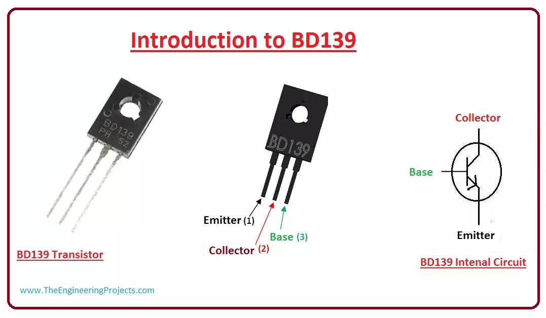
Hello friends, I hope you all are doing great. In today's tutorial, we are gonna have a look at detailed Introduction to BD139. BD139 is a Bipolar NPN transistor, it is mounted in the SOT-32 plastic package. It is designed for audio amplifier and driver utilizing complementary circuits. BD139 has a gain value of 40 to 160, which determine the amplification capacity of a transistor. It has three main pinouts which are a collector, base and emitter. It is used to control (On/Off) bigger loads that consume less than 1.5A.
BD139 is used in different industrial projects such as RF amplifier and Switching Circuits. In today's post, we will have a look at its pinout, Arduino interfacing, applications, Specifications, etc. I will also share some links whe ...
Hello friends, I hope you are all fine will be doing something interesting in your life. In today's tutorial, we are gonna have a look at detailed Introduction to Arduino Zero. Arduino Zero is a Microcontroller device. It is a 32-bit extension of UNO series. Its main features are Atmel Embedded Debugger (EDBG), it provides a full debug interface without additional hardware. This board provides a platform of new inventory projects in smart IoT devices, high technology automation, robotics and much more.
As, Electronic devices coming in our life, they have become cheaper and performing more functions then there predecessor. The microcontroller was introduced in the industry to make our task easy in electronic devices and projects. Arduino Zero is a ...
Hello friends, I hope you all are doing great. In today's tutorial, we are gonna have a look at a detailed Introduction to nRF52840. nRF52840 is a low-power 2.4 GHz wireless system-on-chip (SoC). It integrates a multi-protocol 2.4 GHz transceiver, an Arm Cortex-M4F CPU and flash memory. It is the best system-on-chip (SoC) for any short-range wireless personal area network or IPv6-enabled automation applications.
nRF52840 supports low energy Bluetooth, 802.15.4, ANT™ and user proprietary 2.4 GHz protocols. nRF52840 is used in different industrial projects such as industrial mesh networks, advanced personal fitness devices, and smart city infrastructure. In today's post, we will have a look at its working, specifications, applications, pinout, etc. I will also share some links where I have ...
Hello friends, I hope you all are doing great. In today's tutorial, we are gonna have a look at detailed Introduction to ACS712. ACS712 is an AC or DC current sensor, which is used to measure AC or DC current. You should also have a look at Difference between AC & DC Power, that will help. The maximum value of AC and DC which can be measured is 30A, its output current signal can be read via analog I/O port of Arduino. It is also available in 5A and 20A version which provides precise and economical solutions for AC or DC current sensing in industrial and commercial systems.
ACS712 consists of a precise and low offset linear Hall sensor circuit with a copper conduction path located near the surface of the die. ACS712 is used in different industrial projects and commercial electr ...
Hello friends, I hope you all are doing great. In today's tutorial, we are gonna have a look at a detailed Introduction to DS3231. DS3231 is a real-time clock (RTC) with an integrated temperature-compensated crystal oscillator. It consists of a battery that provides supply to DS3231 when the main supply is off. In this way, it continues working without any interference. It is available in industrial and commercial temperature ranges. It exists in a 16-pin, 300-mil SO package.
DS3231 is used in industrial projects and different electronic devices such as laptops, computers, and GPS for high accuracy of time. In today's post, we will have a look at its working, pinout, applications, protocol, etc. I will also share some links to projects where I have interfaced it with some oth ...