Hello friends, I hope you all are doing great. In today's tutorial, we are gonna have a look at detailed Introduction to PN2222. The PN2222 is a conjoint NPN bipolar junction transistor which is used for common persistence less power intensifying or swapping circuits applications. It is intended for low to intermediate current, squat power, intermediate voltage and can activate at a temperately higher speed. It was initially prepared in the TO-18 metallic cascading.
It is reflected as a very communal transistor and used as a replacement of NPN transistors. It is normally used as a lesser signal transistor and it vestiges a small common persistence transistor of permanent reputation. In today’s post, we will have a look at its cover, specks, associ ...
Hello friends, I hope you all are doing great. In today's tutorial, we are gonna have a look at detailed Introduction to S8550. S8550 is a PNP transistor henceforth during reverse biasing both the collector and emitter will be open and during forward biasing these will be closed. The value of gain is 300 this value governs the magnification ability of the transistor. Its gain is very high therefore it is used for magnification solicitations.
When it is completely biased it can permit a maximum 700mA current to drift crosswise the collector and emitter. This phase is named as Saturation Region and the distinctive voltage permitted across the (VCE) or (VCB) can be 20V and 30V correspondingly. In today’s post, we will have a look at its protection, ...
Hello friends, I hope you all are doing great. In today's tutorial, we are gonna have a look at detailed Introduction to 2sa1943. The 2sa1943 is a high power consuming PNP transistor, firstly it was created by a famous company Toshiba. As it has a high gain of current and consumes higher current at collector it is mostly used for such audio circuits which consume higher power or in AF amplifiers.
Nonetheless, currently the Transistor is outright from Toshiba and it has been swapped with TTA1943. We can also found old 2sa1943 in marketplaces because still it is replicated by other assemblers in China. In today’s post, we will have a look at its fortification, wreckages, implication, proposals, etc. I will also share some links where I have connecte ...
Hello friends, I hope you all are doing great. In today's tutorial, we are gonna have a look at detailed Introduction to MCP23008. MCP23008 provides an 8-bit parallel input/output expansion for I2C bus and SPI applications. It has 8-bit configuration registers for input, output and polarity changing. The master device can enable input and output pins of MCP23008 by writing the Input/output configuration bits. A polarity of the input port register can be inverted with the polarity of the inversion register and all registers can be read by the system master.
MCP23008 is used in different industrial and class projects where I2C and SPI interfacing is required simultaneously. In today's post, we will have a look at its pinout, features, specifications ...
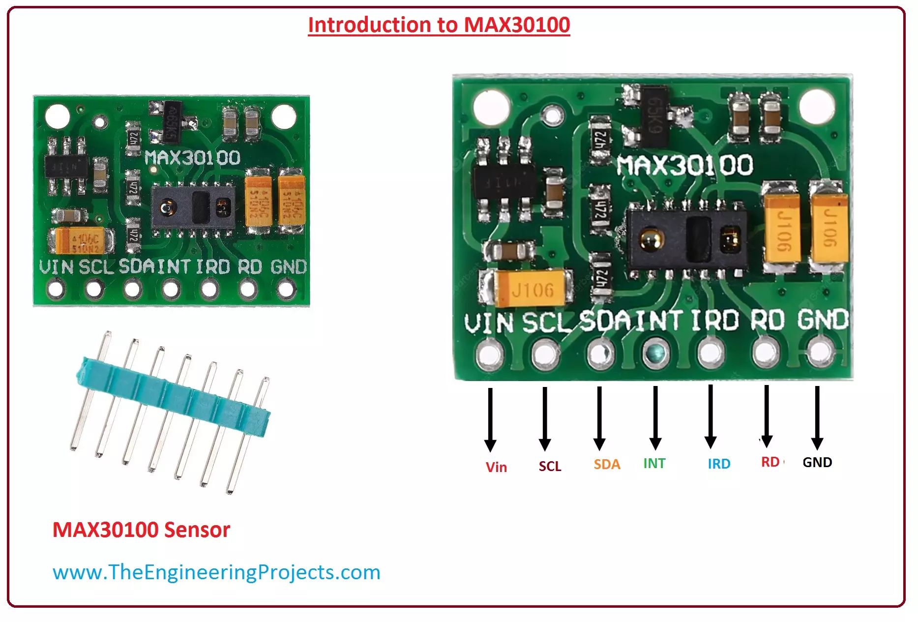
Hello friends, I hope you all are doing great. In today's tutorial, we are gonna have a look at a detailed Introduction to MAX30100. MAX30100 is a heart pulse rate monitor sensor. This sensor consists of two Light Emitting Diodes (LEDs), (one emits infrared light and the other emits red light) modifiable optics, low noise signal processor that detects heart pulse rate signal. Its operating voltage is from 1.8v to 3.3v.
The MAX30100 is used in different industrial and medical equipment such as fitness measurement devices, medical devices, and different wearable instruments. In today's post, we will have a look at its working, pinout, protocol, features, etc. I will also share some links where I have interfaced it with other microcontrollers. If you have any questions about it please ask ...
I hope you all are doing great. In today's tutorial, we are gonna have a look at detailed Introduction to ESP-01. ESP-01 is an inexpensive, small-sized WiFi module, which consists of TCP/IP stack along with a built-in microcontroller. So, we can directly program this small chip and can bring WiFi capability in our Embedded projects. When first time this ship came into the market in August 2014, it got a lot of attention by users. The main reason for it to seek attention is that this module allows the microcontroller to connect with a WiFi available (and programmed to connect) and it follows Hayes Style Commands and develops a TCP/IP network.
ESP-01 chip integrates an antenna, RF balun, power amplifier, filters, and power arrangement module. ESP-01 is used in industry and many projects a ...
Hello friends, I hope you all are doing great. In today’s tutorial, we are gonna have a look at detailed Introduction to RN4020. RN4020 is a completely licensed Bluetooth category 4.1 low energy consuming unit. This module is surfaced with the Bluetooth which is organized by Unpretentious ASCII instructions by UART interfacing. It also comprises all Bluetooth SIG sketches and (MLDP) Microchip low Energy data for customized data.
The scripted features can be secondhand to allow unconnected process without any Microcontroller or mainframe computer. It can be controlled from a distant position by other modules with the protected assembly and it can be reorganized by means of UART interfacing or by air. In today’s post, we will have a look at its casing, pins, structure, applications, ...
Hello friends, I hope you all are doing great. In today's tutorial, we are gonna have a look at detailed Introduction to MPR121. MPR121 is a touch sensor controller, its working is like the capacitor's working principle. This module has twelve electrodes points, it communicates via I2C protocol. When any objects come closer to an electrode point, we can observe the presence of an object by variation in capacitance of an electrode. It's working voltage should be between 2.5 to 3.6 VDC.
MPR121 is used in different industrial projects and electronic devices such as mobile phone and remote control systems. In today's post, we will have a look at its working, pinout, protocol, applications, etc. I will also share some links where I have interfaced it with other microcontrollers. If you have ...
Hello friends, I hope you all are doing great. In today's tutorial, we are gonna have a look at detailed Introduction to A4988. The A4988 is a micro-striding driver for governing the stepper motors, it is incorporated with the interpreter (translator) for the tranquil process. By this controller stepper motor can control by 2 pinouts, one pin is to regulate the direction of motor revolutions and other is for steps regulation of motor.
It works on 3 to 5.5V and it consumes per phase two amperes current in presence of the proper cooling environment. It consists of an immovable off-time current controller which has the capacity to works in sluggish or assorted falling-off styles. In today's post, we will have a look at its cascading, pinout, sorts, uses, etc. I will also share some li ...
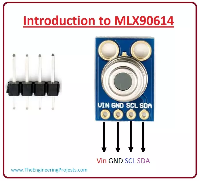
Hello friends, I hope you all are doing great. In today's tutorial, we are gonna have a look at detailed Introduction to MLX90614. MLX90614 is a temperature measurement device works on infrared radiations. It is the best choice for such applications where we can not easily reach to measure temperature because it provides non-contact measurement of temperature. It has Infra Red radiation receptive thermopile and ASSP (Acoustics Speech and Signal Processing) on same TO-39 cascading.
This temperature measuring device is surfaced with the digital Pulse width Modulation and System Managing Bus. It is used in different industries to measure and control the temperature of moving components of machines and it also used to remove the fog on the window of vehicles. In today's post, we will have a ...