What is Bistable Multivibrator

Hello friends, I hope you all are doing great. In today’s tutorial, we will have a look at What is Bistable Multivibrator and how it can be used in different circuits. In this type of multivibrator, the circuitry can operate in any state according to a signal provided at its input while it does not happen in a monostable multivibrator. This arrangement is also defined as a flip flop because flip flop also operates at more than one condition. It also has the ability to store a single bit of information so it is mostly used in logic circuits and in computer data storage part.

This vibrator like other vibrators is used for the production of square waves with providing some delay. These circuits are constructed with numerous kinds of semiconductor components. The most used semiconductor device circuits are operational amplifiers. In today's post, we will have a look at its working, construction, applications and different parameters related to it. So let's get started with What is Bistable Multivibrator.

What is Bistable Multivibrator

  • Bistable Multivibrator has 2 operating conditions so it is called bistable, it is also known as a 2-shot multivibrator.
  • Due to working at two different modes it needs 2 input signal for shifting from one operating mode to others.
  • When first input signal is provided it shifts its operation to second state when second signal provided it come back to previous state.
  • Its another name is flip-flop multivibrator because like flip flops its changes its operation state and regain it after some interval.
  • In the given figure, its structure is shown that consists of 2 NPN transistors that is denoted as Q1 and Q2.
  • At both of these transistors collector 2 loads resistors, RL1 and RL2 are attached.
  • The output terminal of the first transistor is connected with the input of the second transistor through resistor R1 and output of the second transistor is provided at input of first transistor through the resistor R2.
  • Both of the resistance R1 and R2 are connected with a capacitor in parallel. The purpose of these two capacitors is to enhance the switching feature of circuitry so they are also known as commutating capacitors.

Bistable Multivibrator Working

  • Now we discuss the working of this vibrator, for this, we discuss the circuitry that given below figure its construction and components we already discuss so now we the working of these components.
  • When input power is provided to the input terminals of first transistor-transistor starts its operation due to a difference in its feature than the other transistor.
  • When it first transistor starts its operation it goes into saturation state. Due to this value of voltage decreases at the collector terminals.
  • As we know the collector of Q1 is connected with the base terminal of a second transistor due to this it goes into the cutt-off region.
  • Then the voltage at the collector increases to Vcc, this increment in voltage causes to further saturate the first transistor as this voltage is connected with base of Q1 through the resistance R2.
  • It is the first operating condition of bistable multivibrator in which first transistor Q1 is in working state while Q2 is off.
  • This first condition continuous to that point we do not provide the negative signal to first transistor Q1 and positive polarity to transistor Q2.
  • Now if we provide the positive polarity signal to the second transistor Q2 by the capacitor C2 connected with it.
  • This Process will change the second transistor Q2 from saturation mode to cut-off mode, and voltage will decrease at a collector of Q2.
  • As the collector of transistor Q2 is attached with the base of transistor Q1 with the decrement in the voltage at the collector of causes to decrease voltage at transistor Q1 base.
  • This cause to the second transistor obtain saturation state and it is the second operation mode of this module in which the first transistor is off and second is in an operating state.

Bistable Multivibrator Waveform

  • The output waveform generated by the has smaller wavelength or larger according to circuit requirement in rectangle shape.
  • The first end of the rectangle waveform depends on the first input signal and vary according to it and second relies on the second input signal, the resultant waveform is drawn in a given figure.
  • Switching variation among these 2 modes can create bistable circuitry but in some cases it is possible.

TTL Bistable Multivibrators

  • As we above constructed this circuitry by using 2 different transistors now we use integrated circuits for the production this vibrator.
  • The given circuitry explains the circuitry of a bistable vibrator having two NAND gates.
  • This kind of circuits arrangments is known as the Bistable Flip-Flop, in this circuitry, there is a switch that is single pole through a switch (it is such switch that takes one input and can regulate 2 different output). This switch provides logic one and zero to this circuitry.

Application of Bistable Multivibrator

  • These are some applications of the bistable multivibrator.
  • It used in different storage devices and for counting of binary numbers.
  • For frequency division in different circuits.
  • It used for the production of different clock pulses.
  • It used for different relay controller.
  • It used in the different circuit as a toggle switch.

That is complete post on bistable multivibrator I have mentioned each and everything related to this module in this tutorial.

What is Monostable Multivibrator

Hello fellows, I hope you all are doing great. In today’s tutorial, we will have a look at What is Monostable Multivibrator. It is a simple electronic circuit, used to produce a pulse at its output also known as one shot. It generates output pulses according to corresponding circuitry requirements. Its main feature is that after the generation of the output pulse, it regains its stable state and does not produce any further output pulse till not triggers again.

This circuitry can be considered as a biased form of multivibrator (such circuitry that is used for implementation of 2-state modules like timers) that is (on) operating in the starting condition till the triggered point and then becomes unstable on its own. In today's post, we will have a look at its circuitry, construction, working and related parameters. So let's get started with What is Monostable Multivibrator.

What is Monostable Multivibrator

  • Monostable Multivibrator is used for the generation of a square waveform in electronic circuitry.
  • This wave generator belongs to a group of wave generators known as Relaxation Oscillators.
  • It has a simple circuit where 2 switching circuits are designed using transistors(acting as a switch).
  • The transistors are assembled in a way that the output of one transistor is the input of the second transistor.
  • This circuitry also consists of a capacitor and resistor network to create feed-back tank circuitry.
  • There are 2 different working conditions in any multivibrator circuit but monostable has only one 'on' state.
  • This vibration generator comes back to its original condition after a set time of resistor-capacitor circuitry.
 

Construction of Monostable Multivibrator

  • In its construction, 2 transistors are connected in such a configuration that both of these operate as input and output providers to each other.
  • The collector (c) of the first transistor is linked with the base (b) of the second through a capacitor denoted as C1 and base terminal of first transistor that denoted as Q1 is attached with a collector of second transistor by the resistance R2 and capacitor.
  • A direct current source is connected with base (b) point of first transistor by the resistance R3. The input pulse is provided to base (b) of first transistor with the capacitor denoted as C2.
  • In figure resistance, (RL1) and resistance (RL2) is the load connected with these two transistors.
  • When any transistor goes into stable state, then at input pulse is provided to vary its condition. With variation in condition, transistor stays in this condition for time interval set by the resistance-capacitor time constant then get the earlier condition.

Monostable Multivibrator Waveform

  • This wave generator produces a waveform of rectangle shape having low and higher amplitude, the first end of this wave generates with the input trigger signal and the second end generates resistor-capacitor time constant.
  • This resistance-capacitor time constant changes its value to generates large no of pulses that have a specific time interval between them by following the trigger signal provided at input. This assembly is shown in a given figure.
  • The resistor-capacitor time of this vibrator can be change by changing the capacitance of capacitor or resistance value of both.
  • The circuits also have the ability to do increment in the dimensions of a wave as the frequency of output wave remains similar to input signal the difference between them is the width of the waves.

TTL Monostable Multivibrators

  • Above we discussed that this vibration generator can be constructed from individual elements like a transistor, but it can also be manufactured by different ICs.
  • This given circuitry explains how the using only two NOR gates we can construct monostable vibrator.
  • As we are familiar with the operation of NOR gate that its input is low than output will be high and if input is high then the output will be low (0).
  • So at the start, the input is 0 then the output will be higher mean '1'.
  • The resistance Rt linked with the input is also at a high level '1' it means that the quantity of charge at the plates of capacitor is similar.
  • The voltage (V1)  is equivalent to this voltage so the output of NOR is at level 0.
  • If the positive signal is provided to the input at a time (t=0) then the output of NOR gate will be '0' due to this the capacitor will get a discharge.
  • Due to the discharging of the capacitor, the input of second NOR gate is '0'  that converts into high output '1'. This condition is called second condition of circuitry, in which output voltage is equivalent to (+Vcc).
  • This condition continuous on second NOR gate until the capacitor does not get charged again.

Applications of Monostable Multivibrator

  • These are some important applications of Monostable Multivibrator that are described here.
  • Due to time delay capability, it is mostly used in different timer circuits.
  • It also used in different storage circuits.
  • It also used to provide input to other pluse generator circuits.
  • It also has ability to reproduce damage pulses again.

Advantage of Monostable Multivibrator

  • These are some benefits of this pulse generator over other pulse generation modules.
  • It needs only one single pulse to start its operation there is no need of extra pulse for its operation.
  • Its construction is very simple and can be constructed easily.
  • Due to simple construction its price is also less.

So, this is the complete article on  Monostable Multivibrator if you have any questions about it ask in the comments. I will solve your problems. Thanks for reading.

Introduction to TIP122

Hello friends, I hope you all are doing great. In today's tutorial, we are gonna have a look at detailed Introduction to TIP122.  It is a Darlington braces NPN transistor. It works like an ordinary NPN transistor, but as it consists of a Darlington pair it has a decent collector current assessment of nearby 5 amperes and it's gain is around 1000. This transistor can bear 100 volts around collector and emitter terminals due to this feature it can be used for high loads. This is a common purpose transistor it used in different industrial projects. It manufactured for less time taking switching submissions. In today’s post, we will have a look at its protection, wreck, distinction, entitlements, etc. I will also share some links where I have connected it with other microcontrollers. You can also get more material about it in comments, I will guide you more about it. So, let’s get started with a basic Introduction to TIP122. 

Introduction to TIP122

  • It is a Darlington braces NPN transistor. It works like an ordinary NPN transistor, but as it consists of a Darlington pair it has a decent collector current assessment of nearby 5 amperes and it's gain is around 1000.
  • This transistor is famous for its higher gain of current which 1000 and it uses higher current at collector which is 5 amperes.
  • Due to its higher gain of current and huge collector current (IC), it is used in such loads which use higher current and its uses for such submissions which required higher amplification.
  • This transistor consumes less voltage only five volts across base and emitter, therefore, it can be effortlessly organized by a Logical expedient such as a microcontroller.
  • Though precaution has to do to check if the logic expedient can supply up to 120 mA.
  • So, if you are eyeing for a transistor which can be effortlessly organized by a Logical expedient to modification high power consuming loads or to intensify higher current then this transistor can be a perfect option for your solicitations.

    Pinout of TIP122

  • These are the main pinout of TIP122:
Pin# Type                                         Parameters
Pin#1 Emitter Current comes out by the emitter, it is usually linked to ground.
Pin#2 Base It governs the biasing of the transistor and works to turn ON or OFF the transistor.
Pin#3 Collector Current movements in over collector, usually linked to load
Let's see a diagram of the TIP122 pinout:

Features of TIP122

  • These are the main features of TIP122.
    • It is presented in TO-220 Compendium.
    • It is a Darlington Intermediate power consuming NPN Transistor.
    • It has Greater DC Current Gain, which value is 1000.
    • Its Nonstop Collector current (IC) is 5A.
    • Its voltage transversely collector and emitter are 100 volts.
    • The collector and base (Vce) voltage are 100 volts.
    • The quantity of (VBE ) is 5 volts.
    • The value of the current at the base is 120 milliampere.

Working of TIP122

    • This transistor is recognized for its higher current gain which is 1000 and higher collector current 5 amperes, therefore, it is usually used to switch loads with higher current or in submissions which need higher intensification.
    •  This transistor has less base and emitter Voltage of the merely 5V henceforth can be effortlessly organized by a Logic instrument such as a microcontroller.
    • Though precaution has to be engaged to check, if the logic instruments can font up to 120mA.
    • Though TIP122 has extraordinary current at collector and current gain, it is impartially modest to switch the expedient meanwhile it has an Emitter-Base voltage (VBE) of the only 5V and Ib of merely 120mA.
    • In the lower circuit diagram, I have used the TIP122 to control a 48V motor which has an incessant current of around 3A.
    • The incessant collector current of this transistor is 5A and our load devours merely 3A which is well.
    •  The higher base current is around 120 mA, but I have used a higher worth of 100-ohm resistor to bound it to 42 mA.
    • You can also use even a 1K resistor if your collector current prerequisite is fewer.
    •  The highest current of this transistor is 8A so make certain your motor does not devour extra than that.
    •  This is disinterested a perfect circuit figure which displays the employed on this transistor it cannot be used as such.

Applications of TIP122

  • These are the main applications of TIP122.
    • It is used to adjustment of high current loads such as 5 amperes.
    • It is used as an average Power switch.
    • It works where higher intensification is desirable.
    • It used for velocity controller of Motors.
    • It used in Inverter and other rectifier circuitries.
So, that was all about TIP122 if you have any question about it please ask in comments. I will reply to you as soon as possible. Thanks for reading.

Analog Flex Sensor Library for Proteus

Hi Friends! Happy to see you here. Thank you for viewing this read. Hope you’re well today. In this post, I’m going to discuss the Analog Flex Sensor Library for Proteus. You should also have a look at Digital Flex Sensor Library for Proteus. I’ve been adding them over the last few days intending to design and share brand new libraries that are not a part of the proteus library database already. I’m adding both simple simulation and simulation with the Arduino board to help you better understand these libraries with microcontrollers and Arduino devices. Before I go further and walk you through on how to download and simulate Analog Flex Sensor Library for Proteus, let’s get to know what’s Flex sensor first. Simply put, a flex sensor is used to monitor the value of bend. It is also known as a bend sensor that is mainly used in robot whisker sensors, door sensors, stuffed animal toys, and Nintendo power glove. The flex sensor is coupled with the exterior where the rotation of this exterior is directly related to the change in the sensor resistance. Carbon or plastic material is used for the construction of these sensors where deflection value is sensitive to varying resistance. In terms of varying resistance and size, these sensors are categorized into two main types i.e. 4.5-inch bend sensor and 2.2-inch bend sensor. I hope you’ve got a brief insight into what is flex sensor and why it is used for. You can also sneak into the Analog PIR Sensor Library for Proteus that I’ve shared previously. And if you don’t have proteus software installed in your system, check this post on how to download and install proteus software. Without further ado, let’s jump right into the Analog Flex Sensor Library for Proteus. Continue reading.

Analog Flex Sensor Library for Proteus

First of all, click the link given below to download the analog flex library for proteus. Analog Flex Sensor Library for Proteus As you download this file, it contains two folders named Proteus Library and Proteus Simulation. Click the Proteus Library, it will open up four files that read:
  • FlexSensorAnalogTEP.HEX
  • FlexSensorTEP.HEX
  • FlexSensorTEP.IDX
  • FlexSensorTEP
Copy and place these four files into the proteus library folder. Now, click the ‘P’ button as below and write ‘Flex sensor analog’ in the search bar. As you do this, it will return the file as mentioned below.
  • Select this file and click “OK” As you click OK, your cursor will start blinking with the flex sensor, indicating you can place this sensor anywhere you want on the proteus workspace.
When you place this sensor on the proteus workspace, it will appear as follows: This is how flex sensor appears on proteus workspace.

Flex Sensor Pinout

Flex sensor contains four pins as follow:
  • G = first is the ground pin that you’ll connect to the ground voltage.
  • O = second is the OUT pin that gives the Flex sensor value demonstrating if the sensor has identified the value of bend.
  • V = third is the voltage supply pin that receives 5V to power the sensor.
  • TestPin = forth is TestPin that we require in Proteus simulation only. This pin is not included in the sensor in real. We need to add this pin for identifying the value of bend. When this Pin is HIGH it gives the value of bend and when it turns LOW it gives no value of bend.

Adding HEX File

Now we’ll add the HEX file in the Flex sensor to run our simulation. You can find FlexSensorAnalogTEP.HEX file in the library folder of your Proteus library folder. Recall, we’ve already placed this file in the library folder of proteus.
  • To add this file, right-click on the sensor and look for ‘edit properties.’
  • You can also double click the flex sensor to reach the ‘edit properties’ panel.
Now search for the HEX file that you have placed in the proteus library folder. Add this file and click ‘OK’ … Before you run this simulation we need to design and connect the LC circuit with the Flex sensor. We’ll add this circuit purposely. Why? You’ll get to know later in this post. Connect the Output ‘O’ pin with the LC circuit through voltmeter where we get the output voltage following the variable resistor attached with the test pin.
  • Both output voltage across voltmeter and variable resistance are inversely proportional to each other. When resistance is maximum, the voltage on the voltmeter is zero, thus indicating no amount of bend.
And when resistance is zero the voltage appearing across a voltmeter will be 4.98V, confirming the value of bend as an output voltage on the flex sensor. You may be wondering why we add this LC circuit with the flex sensor? We need to include this circuit because proteus gives a peak to peak value that we have to convert into the Vrms value. That LC circuit serves this purpose. You’ve done it. You have designed a simple simulation of a flex sensor library for proteus. We have added this library the very first time, as you won’t find this library in the proteus library database before. I’ve mentioned at the start of the article, I’ll share both simple simulation and simulation with Arduino Board.

Analog Flex Sensor With Arduino UNO

Now we attach the Arduino board with the flex sensor. To do this, we connect the voltage appearing across the voltmeter with the analog input pin of the Arduino board. As you run this simulation it will return the result below. Again, when resistance is maximum, the voltage is zero, that gives equivalent analog value on the LCD connected with the Arduino board, that value is 0019. And when resistance is zero, the voltage will be 4.98V and its equivalent analog value on the LCD will appear 1019. That’s all for today. Hope you find this read helpful. If you face any difficulty in the simulation of Analog Flex Library for Proteus, you can leave your query in the section below, I’ll help you the best way I can. Feel free to leave your suggestions of the libraries that are not available in the proteus library database, I’ll design and share respective libraries with both simple simulation and simulation with Arduino boards. Thank you for reading this post.

Introduction to BC640

Hello Everyone! Hope you’re well today. Thank you for viewing this read. In this post today, I’ll be discussing the Introduction to BC640. BC640 is a bipolar junction transistor that belongs to the PNP transistor family. It is composed of silicon material and comes in a TO-92 package. It is used to drive load under 500mA. In this post, you’ll get to know everything related to BC640 covering pinout, working, alternatives, applications, and physical dimensions. Keep reading.

Introduction to BC640

  • BC640 is a PNP bipolar junction transistor mainly used for amplification and switching purpose.
  • It comes with three pins called the emitter, base, and collector.
  • The base is the main terminal responsible for the entire transistor reaction. The small current change at the base terminal is used to control large current across remaining terminals. The reason, it’s also called current controlled device in contrast to FET (field-effect transistors) which is a voltage-controlled device.
  • BC640 carries three layers where one n-doped layer is placed between two p-doped layers.
  • As this is a PNP transistor, here current flows from emitter to collector as opposed to NPN transistor where current flows from collector to emitter.
  • Both holes and electrons play a critical role in conductivity. In the case of PNP transistors, holes are the majority carriers and electrons are major charge carriers in NPN transistors.
  • It is important to note that NPN transistors are preferred over PNP transistors because the movement of electron is better and faster than the movement of holes. In some electronic projects, both PNP and its complementary NPN are combined and incorporated into a single circuit.
  • When two diodes are joined together from the cathode side, they produce PNP transistors. Here N-layer represents the base terminal while remaining layers represents emitter and collector respectively.
  • In PNP transistor there is no current at the base side when the transistor is turned ON, while in NPN transistor electrons start flowing through the base terminal when the bias voltage is applied.
 
Where To Buy?
No.ComponentsDistributorLink To Buy
1BC640AmazonBuy Now

BC640 Datasheet

  • It’s always better to sift through the datasheet and get a hold of the main features of the component.
  • Download BC640 datasheet by clicking the button given below:
Download BC640 Datasheet

BC640 Pinout

BC640 carries three pins named: 1: Emitter 2: Base 3: Collector The following figure shows the pinout of BC640.
  • All these pins are used for the external connection with the electronic circuits, and they all are different in terms of their functions and doping concentrations.
  • The doping concentration in the emitter terminal is higher than both base and collector terminals.

BC640 Working Principle

  • Both PNP and NPN transistors almost work similarly with some exceptions.
  • The voltage polarities and current directions in PNP transistors appear opposite compared to NPN transistors.
  • The base is still considered the main area responsible for the overall transistor action.
  • As holes are majority carriers in this PNP transistor, now holes are emitted from the emitter terminal (electrons are emitted from the emitter in case of NPN transistor) which are then collected by the collector.
  • It is important to note that when there is no current present at the base terminal, PNP transistor is turned ON and when current flows through the base it is considered turned OFF.

BC640 Power Ratings

The following image shows the absolute maximum ratings of BC640.
Absolute Maximum Ratings BC639
No. Rating Symbol Value Unit
1 Collector-Emitter Voltage Vce 80 V
2 Collector-Base Voltage Vcb 80 V
3 Emitter-Base Voltage Veb 5 V
4 Collector Current Ic 500 mA
5 Total Device Dissipation Pd 625 mW
6 Transition Frequency ft 50 MHz
7 Storage Temperature Tstg -55 to 150 C
  • Both collector-emitter and collector-base voltages are 80V while the emitter-base voltage is only 5V which means the only 5V is required to trigger the transistor reaction.
  • Device dissipation is 625mW which implies the amount of heat it produces as a byproduct due to its primary action.
  • Collector current is 500mA which projects the value of load it can drive. The transition frequency is 50MHz which is a measure of the high-frequency operating characteristics of a transistor.
  • These are the stress ratings. Make sure these ratings don’t surpass the absolute maximum ratings, else they will damage the component, thus the entire project.
  • Moreover, extended exposure to stresses above recommended absolute maximum ratings can influence the device reliability.

Difference between PNP and NPN transistors

  • Current direction is the major difference in both NPN and PNP transistors.
  • Recall, current flows from emitter to collector in PNP transistor when a negative voltage is applied to the base terminal and current flows from collector to emitter in NPN transistor when a positive voltage is applied at the base terminal.
  • In both cases, the base terminal is responsible for the electron reaction.
  • In NPN transistor, the transistor turns on when current flows through the base terminal, and in case of PNP transistor, the device turns on when there is no current at the base terminal.
  • Both transistors are the primary components used in modern electronic projects.
  • It is important to note that both NPN and PNP transistors are interchangeable and are made up of two back to back diodes where one is forward biased and the other is reverse biased.
  • The main difference stands in the polarities of the applied voltage at the base terminal and current direction as mentioned above.
  • In conclusion, both PNP and NPN are interchangeable and work perfectly well if we change the polarity of the applied voltage.

BC640 Alternatives

Following are BC640 alternatives:
  • BC618
  • BC635
  • BC636
  • BC637
Better check the pinout of the alternatives before embedding them into your projects, as it’s likely they might carry different pinout than BC640. The complementary NPN transistor to the BC640 is BC639.

BC640 Applications

The following are some applications of the BC640.
  • It is used to source current, i.e. current flows out of the collector.
  • Used for switching and amplification purpose.
  • Used in electronic motors to control current.
  • Employed in the push button.
  • Used in robotics and instrumentation.
  • Finds applications in Darlington pair circuits.

BC640 Physical dimensions

The following figure shows the physical dimensions of the BC640. That’s all for today. I hope you’ve got an insight into the Introduction to BC640. If you have any question, you can approach me in the comment section below, I’d love to help you the best way I can. You’re most welcome to share your feedback and suggestions, they help us provide quality work. Thank you for reading this post.

Soil Moisture Sensor Library For Proteus

Update: We have created a new version of this library, which you can check here: Soil Moisture Sensor Library for Proteus V2.0.

Hi Friends! Hope you’re well today. I welcome you on board. In this tutorial, I’ll be discussing the Soil Moisture Sensor Library for Proteus. You won't find Soil Moisture Sensor Library in Proteus and we’re going to share its Proteus Library very first time. I have previously shared many Proteus Libraries for digital and analog sensors and today I’m discussing something new. Excited to get a hold of the Soil Moisture Sensor Library? Me too. In the upcoming days, I’ll keep sharing different libraries related to sensors. If you’re curious to sneak into the nitty-gritty of sensors not available in the Proteus library already, pop your suggestion in the comment section below. I’ll try my best to comply with your suggestions and walk you through something brand new.

Soil moisture sensors are used to measure the water content in the soil. They use capacitance to measure the dielectric permittivity of the soil which defines the function of the water content. Before further ado, let’s dive in and have a look at How to download and simulate Soil Moisture Sensor Library for Proteus:

Where To Buy?
No.ComponentsDistributorLink To Buy
1LCD 20x4AmazonBuy Now
2Arduino UnoAmazonBuy Now

Soil Moisture Sensor Library For Proteus

  • You can download the Proteus Library zip file of Soil Moisture Sensor Library by clicking the button below.
Download Proteus Library Files
  • It’s a .zip file that contains two folders inside i.e. Proteus Library & Proteus Simulations.
  • The real fun starts right here right away.
  • Open proteus library folder that contains three files named:
    • SoilMoistureSensorTEP.IDX
    • SoilMoistureSensorTEP.LIB
    • SoilMoistureSensorTEP.HEX
  • Copy and paste these three files in the Library folder of your Proteus software:
  • Now, we need to run the Proteus ISIS software and don't forget to restart, if it's already open.
  • Look for the Soil Moisture in the component’s search box as shown below.
  • After installing the Library successfully, you’ll get similar results as below:
  • You can see in the figure above we have one Soil Moisture Sensor.
  • Now simply place this Soil Moisture Sensor in your Proteus workspace, as mentioned below:
  • You can see in the figure above, I have placed one Soil Moisture Sensor inside the Proteus workspace.
  • This sensor carries 4 pins in total, named:
  • V (Vcc): We’ll provide +5V here.
  • G (GND): We’ll provide ground here.
  • Ao (Out): It’s an analog output signal from the sensor.
  • TestPin: It is used for simulation purposes only. Soil Moisture Sensor doesn’t contain this pin in real.

Adding Sensor’s Hex File

  • After this drill, we’ll add the Sensor’s Hex File, which we have downloaded and placed in the Library folder.
  • To do that, right-click on your Soil Moisture Sensor and then click on “Edit Properties” as below:
  • Or you can double click the Soil Moisture Sensor, it will pop the window below:
  • Click on the Browse button and add SoilMoistureSensorTEP.HEX file available in the Proteus Library section as shown in the figure below:
  • After adding the Sensor’s Hex File, click on the ‘OK’ button to close the ‘Edit Properties’ Panel.
  • Our Soil Moisture Sensor is now ready to simulate in our Proteus ISIS.
  • We’ll design a small circuit to thoroughly understand the working of this Soil Moisture Sensor.

Proteus Simulation of Soil Moisture Sensor

  • Here, I’m designing a simple circuit. I’ve attached a variable resistor with the Test Pin & added a Voltmeter at the Output pin, as shown in the figure below:
  • This resister defines the soil water content in the proteus simulation.
  • When the resistance is maximum at the test pin, the circuit shows zero volts across the voltmeter, which means the sensor is either in the dry ground or taken out of the ground i.e. giving zero moisture value of the water content.
  • And when resistance is zero, the circuit will show the maximum voltage across the voltmeter which indicates the sensor is inserted in a wet ground i.e. water contents in the soil are too high.
  • This is important. We have attached the output pin with an LC filter. This filter is not required in real hardware implementation.
  • We are using it in Proteus Simulation only as Proteus gives the peak-to-peak value and we have to convert that PP value into Vrms.
  • If you are working on a real sensor then you don’t need to add this LC circuit.
  • Now, let’s run this Proteus Simulation and if you have done everything as mentioned, it will show the result mentioned in the figure above.

Simulation of Soil Moisture Sensor with Arduino

Now, let's interface this sensor with a microcontroller.
  • We have attached the output of the sensor appearing across the voltmeter with the A0 pin of the microcontroller as below.

You can see we get the analog value 1019 when the voltage across the voltmeter is 4.98V

This is it. I hope you find this tutorial helpful. This will help engineering students in simulating their semester projects in proteus. In the next tutorials, I’ll be sharing and adding more libraries of sensors. You’re most welcome to share your suggestions with the sensors you want me to libraries of. If you’re unsure or have any questions, you can ask me in the section below. I’ll help the best way I can. Thank you for reading this article.

Introduction to BC327

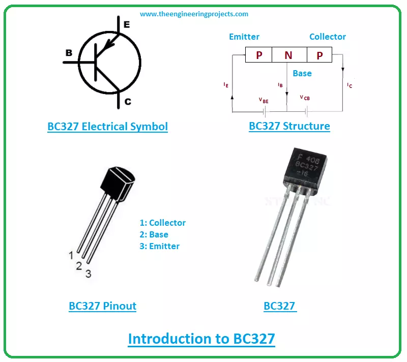
Hi Friends! Glad to see you here. I welcome you on board. In this post today, I’ll be discussing the Introduction to BC327. BC327 is a bipolar junction transistor that falls under the family of PNP transistors. It is composed of silicone material and is used to drive load under 800mA. It’s a current-controlled device that carries three pins where small current generated at the one terminal is used to control large current at the other terminals. Read this post all the way through as you’ll get to know all nuts and bolts of BC327 covering pinout, working, power ratings, applications, and physical dimensions. Let’s get started.
Where To Buy?
No.ComponentsDistributorLink To Buy
1BC327AmazonBuy Now

Introduction to BC327

  • BC327 is a PNP bipolar junction transistor that comes in the TO-92 package and is used for switching and amplification purpose.
  • It comes with three pins named emitter, base, and collector that are mainly used for external connection with the electronic circuit.
  • BC327 is incorporated with three layers where one n-doped layer is sandwiched between two p-doped layers. The n-doped layer is negative while the p-doped layer is positively charged.
  • This transistor incorporates 800mA collector current, hence it is easily employed to drive a variety of heavy loads.
  • Collector dissipation is 625mW while the maximum current gain is 630 which makes it a suitable pick for audio amplification purposes.
  • Transistors are mainly divided into two types named NPN and PNP transistors this BC327 transistor belongs to the PNP transistor family.
  • Both transistors are different in terms of their charge carriers used for conductivity.
  • Electrons are major carriers in NPN transistors while holes are major carriers in PNP transistors.
  • When two diodes are combined from the cathode side, they constitute a PNP transistor where the N-doped layer represents the base side while the other two p-doped layers represent the emitter and collector respectively.
  • You know it already, the movement of electrons is far better and faster than the movement of holes. The reason NPN transistors have a leg over PNP transistors for their quick response in conductivity.

BC327 Datasheet

  • To understand the component thoroughly, it’s always wise to sift through the datasheet.
  • Download BC327 Datasheet by clicking the button below:

BC327 Pinout

BC327 comes with three pins named 1: Emitter 2: Base 3: Collector The following figure shows the pinout of BC327.
  • These pins are used for external connection with the electronic circuit. The small current change at the base terminal produces a large current change across other terminals.
  • The base terminal plays a key role in differentiating both NPN and PNP transistors.
  • In NPN transistor current flows through the base side when voltage is applied while in PNP transistor no current flows through the base terminal when the transistor is turned ON.

BC327 Working Principle

  • When current flows through the base terminal in this PNP transistor, the transistor is turned OFF, and on the other hand, when there is no current at the base side, the transistor is turned ON.
  • PNP works the same as NPN transistor but in the opposite fashion. The base still controls the large current across other terminal but here current flows in the opposite direction i.e. from emitter to collector.
  • And instead of electrons emitted in the case of NPN transistor, holes are emitted by the emitter in PNP transistor that are then collected by the collector.

BC327 Power Ratings

The following table shows the absolute maximum ratings of BC327.
Absolute Maximum Ratings BC639
No. Rating Symbol Value Unit
1 Collector-Emitter Voltage Vce 45 V
2 Collector-Base Voltage Vcb 50 V
3 Emitter-Base Voltage Veb 5 V
4 Collector Current Ic 800 mA
5 Collector Power Dissipation Pc 625 mW
6 Junction Temperature Tj 150 ºC
7 Storage Temperature Tstg -55 to 150 ºC
  • These are stress ratings that can make or break your entire project. Make sure ratings don’t exceed these absolute maximum ratings else you may compromise your component.
  • Similarly, if these ratings are applied for more than the required time, they can affect the reliability of the device.

Difference between PNP and NPN Transistors

  • The BC327 transistor carriers the same characteristics as NPN transistors with a few exceptions.
  • In the case of PNP transistors, all current directions and voltage polarities will be reversed compared to NPN transistors.
  • The NPN transistor sources current through the base terminal while PNP sinks current into the base terminal, the reason it’s also called a sinking device.
  • In PNP transistor the base terminal is more negative than the emitter terminal. And all these terminals are different in terms of their doping concentration.
  • The emitter terminal is highly doped and comes with 100% current of the transistor while the base terminal is lightly doped and is responsible for the transistor action and controls the number of holes emitter from the emitter which are then collected by the collector.
  • The collector terminal is bigger compared to other terminal and is lightly doped.
  • Both NPN and PNP also differ with respect to the applied source voltage i.e. in case of NPN transistor source voltage is applied at the collector side while in case of PNP transistor source voltage is applied at the emitter side.
  • A load resistor is also used while working with this BC327 PNP transistor that controls the current in the collector terminal.
  • Plus, biased voltage is applied at the base terminal that initiates the transistor action and it is coupled with the base resistor to resist and limit the current flowing through this terminal.

BC327 Alternatives

The following are alternatives to BC327. The pinout settings of the alternative may differ from the actual BC327. It’s wise to check the pinout of the transistor before employing it in your electronic circuit. NPN Complementary of BC327 is BC337. Since they both form a complementary pair, they can be employed together in many electronic projects.

BC327 Applications

BC327 comes with the following applications:
  • Used for signal amplification and switching purposes.
  • Finds application microcontrollers to drive heavy loads.
  • Used in audio amplifiers and multiple preamplification stages.
  • Employed to drive loads under 800mA.
  • Used in push-pull configuration circuits.
  • Used in medium-speed switching and high-frequency amplifiers.

BC327 Physical dimensions

The following figure shows the physical dimensions of the BC327. That’s all for today. I hope you find this read useful. If you have any questions, you can approach me in the section below. I’d love to help you the best way I can. Keep us updated with your valuable feedback and suggestions, they help us create quality content. Thank you for reading this post.

Introduction to BC550

Hi Guys! Happy to see you here. Thank you for viewing this read. In this post today, I’ll walk you through the complete Introduction to BC550. BC550 is a low-power low-frequency general-purpose bipolar transistor. It is mainly used to drive loads under 100mA. BC550 carries three terminals where a small current across one terminal is used to control the large current across the remaining terminals. It’s primarily used for amplification and switching purposes. Transistors are critical components and building blocks of modern electronic circuits. Bipolar junction transistors are divided into two main types named NPN transistors and PNP transistors. The BC550 falls under the category of NPN transistors and is available in a plastic TO-92 case. I suggest you read this entire post all the way through as you’ll get to know all nitty-gritty of BC550 i.e. datasheet, pinout, working principle, power ratings, applications, and physical dimensions.

Keep reading.

Where To Buy?
No.ComponentsDistributorLink To Buy
1BC550AmazonBuy Now

Introduction to BC550

  • BC550 is an NPN bipolar junction transistor mainly used for switching and amplification purpose.
  • It incorporates three pins called the emitter, base, and collector. Where small current change at the base terminal is used to induce large current change across other terminals.
  • BC550 carries three layers i.e. two N-doped layers and one P-doped layer. The P-doped layer indicates a positively charged layer that stands between the two N-doped layers that are negatively charged.
  • When this transistor acts as a switch it is used to turn ON and OFF the input signal. When a powerful signal passes through the transistor, it turns ON the switch while lack of signal turns the switch OFF.
  • When several thousands of millions of transistors are formed together, they can be incorporated into integrated circuits or in discrete components.
  • BC550 is composed of semiconductor material. Silicon is mostly used to form these NPN transistors.
  • In this NPN transistor, electrons are the majority carriers used for conductivity as opposed to PNP transistors where conductivity is carried out with holes as majority carriers.
  • It is important to note that the movement of electrons is far better and faster than the movement of holes, the reason NPN transistors are better, thus preferred over PNP transistors.
  • The main difference between NPN and PNP transistors is the behavior of the base terminal. In NPN transistors, current flows through the base terminal while in the case of PNP transistors no current flows through the base terminal when a transistor is ON.
  • Also, the current flows from collector to emitter in NPN transistors, and in PNP transistors current flows from emitter to collector.
  • Computer circuit boards are the common example of NPN transistors that carry millions of transistors used to store memory in the form of binary code.

BC550 Datasheet

  • To understand the component thoroughly, it’s always wise to scan the datasheet.
  • You can download BC550 Datasheet by clicking the button below:

BC550 Pinout

BC550 comes with three pins called
  1. Emitter
  2. Base
  3. Collector
The following figure shows the pinout of the BC550:
  • All these terminals are different in terms of their doping and functions.
  • The emitter terminal is highly doped compared to the other two terminals.
  • The emitter emits the electron into the base terminal which controls the number of electrons. The collector terminal is used to collect the number of electrons.

BC550 Pin Configuration

BC550 can be embedded in the following three configurations:
  1. Common emitter configuration
  2. Common collector configuration
  3. Common base configuration
  • Mostly amplification is carried out using a common emitter configuration as it comes with the exact voltage and current ratings required for amplification purposes.
  • The amplification factor is an important factor used to define the nature of amplification. It’s a ratio between collector current and base current and is denoted by ß.
  • The current gain is another factor which is a ratio between collector current and emitter current. It is denoted by a and is known as alpha. The alpha value ranges from 0.95 to 0.99 but mostly its value is taken as unity.

BC550 Working Principle

  • In BC550, the base works as an electron valve that controls the number of electrons. When a voltage is applied across the base terminal, it triggers the electron reaction. Thus, the emitter starts emitting the electrons into the base terminal which are then collected by the collector.
  • A small change in input voltage at the base terminal produces a large change in output voltage across other terminals. This phenomenon is used for amplification purposes.
  • The collector voltage is always positive with respect to the emitter terminal while the base terminal is positive with respect to the emitter.
  • And the collector terminal is combined with the load voltage using a resistor which is used to control the flow of current.

BC550 Power Ratings

The following table shows the absolute maximum ratings of BC550:
Absolute Maximum Ratings BC639
No. Rating Symbol Value Unit
1 Collector-Emitter Voltage Vce 45 V
2 Collector-Base Voltage Vcb 50 V
3 Emitter-Base Voltage Veb 5 V
4 Collector Current Ic 100 mA
5 Collector Power Dissipation Pc 500 mW
6 Junction Temperature Tj 150 ºC
7 Storage Temperature Tstg -55 to 150 ºC
  • Emitter-Base voltage is 5V, which means the only 5V is required to trigger the base terminal, thus the entire transistor. While Collector-Base and Collector-Emitter voltages are 50V and 45V respectively.
  • The collector current is 100mA i.e. it can drive loads with a value under 100mA.
  • It’s wise to do your due diligence before incorporating this tiny device into your project as values exceeding absolute maximum ratings can severely damage the component.
  • Plus, make sure you don’t apply these values for more than the required time, else they can affect the device's reliability.

BC550 Alternatives

BC550 equivalent are: The complementary PNP transistor of the BC550 is BC560. BC550 Applications
  • Used for amplification and switching purposes.
  • Can be employed in the current mirror and H-bridge circuits.
  • Used in linear amplifier and impedance buffering.
  • Finds applications in oscillator and comparator circuits.
  • Used in Astable and Bistable multivibrator circuits.
  • Used for pre-amplification stages in electronic circuits.

BC550 Physical dimensions

The following figure shows the physical dimensions of the BC550: That’s all for today. Hope you’ve got a clear insight into the Introduction to BC550. You’re most welcome to ask your queries in the section below. I’d love to help you the best way I can. Feel free to keep us updated with your valuable suggestions and feedback. Thank you for reading this post.

Introduction to BC639

Hi Friends! Happy to see you here. I welcome you on board. In this post, I’ll walk you through the Introduction to BC639. BC639 is a high current gain bipolar junction transistor that falls under the NPN transistor family. It constitutes a high collector current and low collector-emitter saturation voltage and is widely used for amplification and switching purposes. It is used to drive load under 500mA. Collector Dissipation is 0.625W while DC Current Gain (hfe) ranges from - 40 to 160 with transition frequency 200MHz. In this post, I’m going to discuss all nitty-gritty of the BC639 transistor covering pinout, working, power ratings, alternatives, applications, and physical dimensions. Continue reading.

Introduction to BC639

  • BC639 is an NPN bipolar junction transistor that carries high collector current and low collector-emitter saturation voltage.
  • It is composed of silicon material and comes in a TO-92 package.
  • BC639 carries three pins named emitter, base, and collector.
  • It is mainly known as a current-controlled device where the base terminal is responsible for the entire transistor action.
  • BC639 contains three layers where one p-doped layer sits between two n-doped layers.
  • The small input current change at the base terminal is used to control large output current at the other two terminals.
  • The base terminal controls the flow of electrons and acts as a control value. The emitter terminal emits the electron passing through the base terminal which are then collected by the collector terminal.
  • Both electrons and holes play a critical role in conductivity carried out by these tiny components. In the case of NPN transistor electrons are the major charge carriers while in the case of PNP transistors holes are major carriers.
  • The movement of electrons is faster and better than the movement of holes for conductivity. The reason these NPN transistors are preferred over PNP transistors for the making and execution of electronic projects.
Where To Buy?
No.ComponentsDistributorLink To Buy
1BC639AmazonBuy Now

BC639 Datasheet

  • It’s always wise to scan through the datasheet and get a hold of the main features of the component.
  • Download BC639 datasheet by the link given below:

BC639 Pinout

BC639 comes with three pins called 1: Emitter 2: Base 3: Collector The following figure shows the pinout of BC639. Recall, BC639 is used to amplify the weak signal. As this is an NPN transistor, here current flows from collector to emitter as opposed to PNP transistor where current flows from emitter to collector. All these terminals are different in terms of their functions and doping concentrations. The emitter side is highly doped as opposed to the other two terminals. These pins are used for external connection with the electronic circuits.

BC639 Pin Configuration

BC639 transistor is employed in the following three main configurations:
  • 1: Common emitter configuration
  • 2: Common collector configuration
  • 3: Common base configuration
  • Common emitter configuration is used for the amplification purpose as it contains the suitable voltage and current ratings needed for amplification purposes.
  • The nature of amplification is demonstrated by the amplification factor that is a ratio between collector current and base current. It is denoted by ß.
  • The current gain is another important factor used to describe the nature transistor. It is a ratio between collector current and emitter current. It is called alpha and is denoted by a. The alpha value stands from 0.95 to 0.99 but frequently its value is taken as unity.

BC639 Working Principle

  • It all starts from the base terminal. When the voltage is applied at the base pin, it ignites the electron reaction inside the transistor. This base pin controls the number of electrons emitted by the emitter terminal. The base pin acts as an electron valve and is responsible for conductivity inside the entire component.
  • When BC639 acts as an amplifier, the small current at the base terminal (which acts as an input current) is used to control a much larger electric current at both emitter and collector terminals.
  • And when it operates as a switch, it converts the small current at one part of the transistor into a much larger current across the remaining parts of the transistor.
  • The base pin is positive with respect to the emitter terminal and collector voltage is always positive with respect to the emitter terminal.
  • It’s important to note that the collector terminal is combined with the load voltage using resistor that limits and controls the flow of current.

BC639 Power Ratings

The following table shows the absolute maximum ratings of BC639.
Absolute Maximum Ratings BC639
No. Rating Symbol Value Unit
1 Collector-Emitter Voltage Vce 60 V
2 Collector-Base Voltage Vcb 60 V
3 Emitter-Base Voltage Veb 5 V
4 Collector Current Ic 500 mA
5 Current Gain hfe -40 to 160
6 Transition Frequency ft 200 MHz
7 Storage Temperature Tstg -55 to 150 C
  • Both collector-emitter and collector-base voltages are 60V while the emitter-base voltage is a mere 5V, which means the only 5V is required to trigger the electron reaction at the base terminal. And collector current is 500mA which projects that it can drive load under 500mA.
  • The storage junction temperature range is -55 to 150C. While collector Dissipation is 0.625W and DC Current Gain (hfe) ranges from - 40 to 160 with transition frequency 200MHz.
  • These are stress ratings that define the working of a component under certain values.
  • If these values exceed the absolute maximum ratings, they can damage the component, thus the entire project.
  • Do your due diligence before applying this component into your project and make sure you work under these mentioned ratings.
  • Also, if these ratings are applied more than the required time, they can affect device reliability. Be careful.

BC639 Alternatives

KSC1009C transistor can be replaced by BC639. The complementary transistor of BC639 is BC640.

BC639 Applications

BC639 is used in the following applications:
  • Used for amplification and switching purposes.
  • Used in oscillator and comparator circuits.
  • Employed in the current mirror and H-bridge circuits.
  • Used for pre-amplification stages in electronic circuits.
  • Finds applications in linear amplifier and impedance buffering.
  • Incorporated in oscillator and comparator circuits.
  • Used in Astable and Bistable multivibrator circuits.

BC639 Physical dimensions

The following figure shows the physical dimensions of the BC639. This is it. I hope you find this article helpful. I strive to share easy to read and easy to digest information. If you are unsure or have any question, you can pop a comment below, I’d love to help you the best way I can. Keep sharing your valuable feedback and suggestions, they help us create quality content. Thank you for your precious time.

Introduction to BC549

Hi Friends! I hope you’re well today. I welcome you on board. In this post, I’m going to discuss the Introduction to BC549. BC549 is a general purpose bipolar junction transistor that belongs to NPN transistor family. It contains three pins where small current change in one terminal produces a much large current change across other terminals. In other words, it is nothing but a current booster. It is known as a low power low voltage current controlled device and is used for switching and amplification purpose.  In this article I’ll be discussing complete details of BC549 transistor i.e. pinout, working principle, power ratings, physical dimensions and applications. Stay tuned.

Introduction to BC549

  • BC549 is an NPN general-purpose bipolar junction transistor. It carries three pins named emitter, base, and collector and is available in TO-92 and SOT54 package.
  • BC549 transistor contains three layers i.e. two N-doped layers and one P-doped layer. The P-doped layer stands between two N-doped layers. Plus, it contains two PN junctions where one is forward biased and the other is reverse biased.
  • When no voltage is applied at the base terminal it is considered as grounded. In this case, the transistor acts like an open switch where both emitter and collector remain open.
  • When voltage is applied at the base terminals it gets biased and draws current which is used to connect other terminals and current starts flowing from collector to emitter terminal.
  • As this is an NPN transistor, here current flows from collector to emitter when voltage is applied, unlike PNP transistor where current flows from emitter to collector.
  • Plus, both electrons and holes play a vital role in conductivity. In NPN transistor electrons are majority charge carriers and in PNP transistor holes are majority carriers.
  • The movement of electrons, however, is faster than the movement of holes, the reason NPN transistors are better and faster than PNP transistors.

BC549 Pinout

BC549 comes with three pins named:
  • 1: Emitter
  • 2: Base
  • 3: Collector
Following figure shows the pinout diagram of BC549.
  • All three pins are used for external connections with other circuits. These pins are different in terms of operation and doping concentration.
  • The collector voltage is larger than the base voltage and emitter terminal is highly doped compared to other terminals.

BC549 Pin Configuration

BC549 transistor can be employed in three main configurations as follows:
  • Common emitter configuration
  • Common base configuration
  • Common collector configuration
Common emitter configuration is mostly used for amplification purposes as it contains the exact current and voltage ratings required for amplification.
  • The amplification factor is called beta and is denoted by ß. It is mainly used to define the nature of amplification. It’s a ratio between collector current and base current. In BC549, the amplification factor ranges from 420 to 800.
  • Another important factor is the current gain which is a ratio between collector current and emitter current. It is known as alpha and is denoted by a. The alpha value stands from 0.95 to 0.99 but more often than not its value is taken as unity.

BC549 Working Principle

  • In BC549, emitter-base voltage is 5V which means when 5V is applied at the base terminal it gets biased and triggers the electron reaction.
  • In the NPN transistor, the base terminal behaves like a control valve that controls the number of electrons.
  • When voltage is applied at the base terminal, emitter starts emitting the electrons into the base terminal which controls the number of electrons. These emitted electrons passing through the base are collected by the collector terminal of the transistor.
  • Moreover, the collector current is a mere 100mA i.e. you cannot drive heave loads using this transistor.
  • As the only 5V is required to start the electron reaction at the base terminal, it can be easily employed across microcontrollers and microprocessors.
  • When BC549 operates as an amplifier, small current as an input signal at the base terminal is used to induce a much bigger electric current at the other terminals.
  • And when it works like a switch, it switches the small current at one part of the transistor into a much larger current across the other parts of the transistor.
  • When transistor acts as a switch, it carriers two distinct states i.e. values are stored in the form of zero and one. Memory chip used in a computer is a common example of an electronic device that contains billions of transistors which can be turned on and off individually.

BC549 Power Ratings

Follow figure shows the absolute maximum rating of BC549:
  • Emitter-Base voltage and Collector-Emitter voltages are 5V and 30V respectively.
  • And Collector-Base voltage is 30V with collector current 100mA i.e. it cannot drive loads carrying ratings more than 100mA.
  • The current gain ranges from 420 to 800 and transition frequency is 100MHz.
  • These are stress ratings. Before you employ this transistor into your project and execute, make sure the ratings don’t exceed from absolute maximum ratings, else they will damage the product, and worse, your entire project, eventually.
  • Also, if these ratings are applied for more than the required time, they can affect device reliability.

BC549 Alternatives

The following are the alternatives of a BC549 transistor. The PNP complementary of BC549 are:
  • BC559
  • BC560

BC549 Applications

BC549 can be used in the following applications:
  • Used in liner audio amplifiers.
  • Employed in Darlington pairs and sensor circuits.
  • Used in oscillator and comparator circuits.
  • Finds application in current mirror circuits.
  • Used in Astable and Bistable multivibrators.
  • Used for impedance buffering and switching applications.
  • Finds application in low noise stages in audio frequency equipment.

BC549 Physical dimensions

Follow figure shows the physical dimensions of BC549: That’s all for today. Hope you find this article helpful. If you are unsure or have any question, you can approach me in the section below. I’d love to help you the best way I can. You’re most welcome to keep us updated with your valuable feedback and suggestions, they help us produce quality content. Thank you for reading this article.
Syed Zain Nasir

I am Syed Zain Nasir, the founder of <a href=https://www.TheEngineeringProjects.com/>The Engineering Projects</a> (TEP). I am a programmer since 2009 before that I just search things, make small projects and now I am sharing my knowledge through this platform.I also work as a freelancer and did many projects related to programming and electrical circuitry. <a href=https://plus.google.com/+SyedZainNasir/>My Google Profile+</a>

Share
Published by
Syed Zain Nasir