Introduction to Arduino Nano Every

Hi Guys! I welcome you on board. Thank you for clicking this read. In this post today, I’ll detail the Introduction to Arduino Nano Every. Arduino Nano Every is a tiny powerful board that is based on the ATMega4809 AVR processor. It comes with a clock speed of around 20MHz and flash memory of around 48KB. It carries two 15 pin connectors on each side of the board that are pin-pin compatible with the Arduino Nano Every. The low price and small size make this board an ideal pick for the range of electrical projects like electronic musical instruments, low-cost robots, and general development of the small parts of the large projects. Needless to say, Arduino has been a cornerstone of many electronic projects ranging from simple student projects to complex automation and embedded projects. The working of this tiny beast is simple and straightforward. It takes the input like a finger on a button or light on a sensor and converts it into an output like turning on the motor, activating LED blinking, and something sharing online. You can use Arduino IDE software to program the Arduino board. In other words, you can control the board by sending a lot of instructions to the microcontroller of the board. The Arduino comes with easy to use hardware and software platform that even a non-tech person can get a hands-on experience without having prior technical knowledge about these boards. I suggest you read this post till the end as I’ll walk you through the complete Introduction to Arduino Nano Every covering datasheet, pinout, pin description, features, and applications. Let’s get started.

Introduction to Arduino Nano Every

  • Arduino Nano Every is a tiny powerful board that is based on the ATMega4809 AVR processor.
  • The Arduino Nano Every is almost similar to the Arduino Nano board with the addition of a more powerful processor like Atmega4809.
  • This board comes with more program memory compared to Arduino Uno and RAM is 200% bigger, helping you create a lot of variables.
  • If you’ve used Arduino Nano earlier for your project, you’ll come to know the Arduino Nano Every board is a pin-equivalent substitute of Arduino Nano. The difference lies in the addition of a micro-USB connector and a more powerful processor.
  • Arduino Nano Every is available in two versions: with or without headers, helping you incorporate this board into hard-to-reach places including wearables.
  • No components are available on the B-side, this gives you the ability to solder the board directly into your main PCB design, reducing the height of the entire project.
  • It carries a crystal oscillator with a clock speed of around 20MHz which is necessary to synchronize all internal functions of the board.
  • The SRAM memory is 6KB while the flash memory and EEPROM memories are 48KB and 256bytes respectively.
  • The flash memory is the location where the Arduino program (sketch) is stored. While SRAM is used to generate and manipulate variables when it starts running. And the EEPROM is a non-volatile memory which means data stays stored inside the board even if the board power is removed.

Arduino Nano Every Datasheet

While working with this board, it’s better to look into the datasheet of the board that features the main characteristics of the board. Click the link below to download the datasheet of Arduino Nano Every.

Arduino Nano Every Pinout

The following figure shows the pinout diagram of Arduino Nano Every.   There is a built-in LED at pin 13 and it also features one power LED that turns on when the board is supplied with power.

Arduino Nano Every Pin Description

Still reading? Perfect. I hope you’ve read the brief intro of this Every board. In this section, we’ll highlight the description of each pin incorporated on the board. Let’s get started.

Digital Pins

20 digital I/O pins are incorporated on this device which you can use as an input or output based on the requirements. These pins are either in a HIGH state or LOW state. When they are LOW they receive V0 and when they are HIGH they receive 5V.

Analog Pins

The number of analog pins incorporated on the board is 8. These are analog pins which projects they can receive any number of values in contrast to Digital pins that only receive two values i.e. HIGH or LOW

PWM Pins

The number of PWM pins incorporated on the board is 5. The board creates analog results with digital means when these pins are activated.

I2C Pins

This board incorporates a two-wire communication protocol which is known as I2C protocol. It carries two lines i.e. SCL and SDA. The SCL is a serial clock line mainly used for the synchronization of all data transfer through the I2C bus and the SDA is a serial data line mainly used to carry the data.

SPI Pins

This device comes with SPI (serial peripheral interface) pins that are mainly used to lay out the communication between the controller and other peripheral devices such as sensors or shift registers. There are two pins: MISO (Master Input Slave Output) and MOSI (Master Output Slave Input) used for SPI communication. These pins are employed to receive or send data by the controller.

UART Pins

The UART pins are used for serial communication. It carries two lines Tx and Rx. The Tx is used to transmit the serial data while Rx is used to receive the serial data.

Arduino Nano Every Features

The following are the main features of Arduino Nano Every. Operating Voltage = 5V Microcontroller = Atmega4809 Vin range = 7 to 21 V D/C current per 3.3V pin = 50mA D/C current per I/O pin = 20mA Oscillator = 20MHz EEPROM = 256bytes SRAM = 6KB Flash Memory = 48KB LED_BUILTIN = 13 USB = 1 UART = 1 SPI = 1 I2C = 1 Digital Pins = 20 Analog Pins = 8 PWM pins = 5 Size = 18x45 mm Weight = 5g

Programming

  • Arduino IDE (integrated development environment) is used to program this board. This software is used to program all kinds of Arduino boards.
  • This device contains a built-in Bootloader which is used to burn the program inside the controller. Yes, you don’t need a separate burner to burn and transfer the program into the controller.
  • Moreover, it also carries a micro USB port which is used to connect the device with the computer. Using this port, you can test and run the program directly from the computer.

Difference between Arduino Nano Every and Arduino Nano

  • The Nano carries microcontroller ATmega 328p which is the same as Uno.
  • While the Nano Every and Uno WiFi Rev 2 are incorporated with a modern version of the AVR based MCU known as megaAVR_0-series, an ATmega4809.
  • It carries the same AVR CPU architecture in the base of the MCU so initially, both MCUs (Atmega 328p and Atmega 4809) share the same compiler but there lies a difference in MCU peripherals configuration. So know that the previous knowledge about AVR MCU peripherals won’t help here.
  • The Arduino Nano Every is priced lower than Arduino Nano.

Arduino Nano Every Applications

The small size of this board makes it a good pick for a number of applications. Following are some applications of this board.
  • USB Trackpad
  • Automatic Pill Dispenser
  • USB Joystick
  • Electric Bike
  • Creating a wireless keyboard
  • Water Level Meter
That was all about the Introduction to Arduino Nano Every. If you have any queries, you can approach me in the comment section below. I’d try to help you according to the best of my expertise. Feel free to share your valuable feedback and suggestions around the content we share so we keep producing quality content based on your needs and requirements. Thank you for reading the article.

Introduction to Arduino MKR Vidor 4000

Hey Everyone! Hope you’re well today. I welcome you on board. In this post today, I’ll walk you through the Introduction to Arduino MKR Vidor 4000. The Arduino MKR Vidor 4000 is a powerful board with which you can develop your own controller board. The inclusion of FPGA makes this device unique and separate from other Arduino boards available in the market. With this FPGA feature, you can do audio and video processing which is not possible with other Arduino boards. Using this device, you can design a real-time computer reading sensor information and the best part is this board is compatible with all other Arduino boards. With this board, you can make all pins PWM signals (on the FPGA block side) for handling the speed of motors. Moreover, you can develop a sound effect pedal for your guitar by capturing the sound in real-time. With Arduino IoT cloud, you can also handle the complex laboratory machine connected with a number of motors. Before moving further, I suggest you read the Introduction to Arduino MKR NB 1500 that I’ve uploaded previously. I suggest you buckle up as I’ll walk you through the complete introduction to Arduino MKR Vidor 4000 covering datasheet, pinout, features, programming, and applications. Let’s get started.

Introduction to Arduino MKR Vidor 4000

  • The Arduino MKR Vidor 4000 is a powerful board with which you can develop your own controller board.
  • This board is incorporated with SAMD21 microcontroller and Intel® Cyclone® 10CL016 (FPGA).
  • The inclusion of the most powerful reprogrammable chip FPGA makes this device unique and separate from other Arduino boards available in the market.
  • With this FPGA feature, you can do audio and video processing which is not possible for other Arduino boards.
  • The FPGA carries 504Kbit of embedded RAM, 16K Logic Elements, and 56 18x18 bit HW multipliers that are employed for high-speed DSP (digital signal processing).
  • Every pin is activated at over 150 MHz and normally configured for functions such as (Q)SPI, high res/ high freq PWM, UARTs, quadrature encoder, Sigma Delta DAC, I2C, I2S, etc.
  • Using this Vidor device you can do an experiment with precision as it comes with the RESET button which you can use in case anything goes wrong. As you press and release this button, the board gets reset, helping you program the board from scratch.
  • The operating voltage of this board is 3.3V and one Mini PCI express port with programmable pins is also installed on the board that carries up to 25 user-programmable pins.
  • The board also features a MIPI (mobile industry processor interface) camera connector which is nothing but a set of standards that allow implementing important features of smartphones including displays and imaging devices. In simple words, the MIPI standard is employed to offer connectivity in mobile, multimedia, automotive, augmented reality, and virtual reality, and other related applications.
  • Other features include - Wifi & BLE powered by U-BLOX NINA W102 module, Micro HDMI connector, the MKR interface where all pins are controlled by both SAMD21 and FPGA.
  • The flash memory of FPGA on this Vidor board is 2MB and SDRAM memory is 8MB. There is no EEPROM memory. The flash memory is used to store the Arduino program (sketch) and SDRAM memory is used to produce and manipulate variables when it runs.
  • The flash memory on the microcontroller side is 256KB and the SRAM memory is 32KB. There is no EEPROM memory on the microcontroller side.
  • The power to the board by USB is 5V. Moreover, the board also features a Li-Po charging circuit that runs the board in two ways: either from the external 5V source or from battery power.

Arduino MKR Vidor 4000 Pinout

The following figure shows the pinout diagram of Arduino MKR Vidor 4000.

Arduino MKR Vidor 4000 Pin Description

Hope you’ve got a brief idea about this Vidor board. In this section, we’ll cover the description of each pin installed on the microcontroller block side and FPGA block side. Let’s jump right in.

Digital Pins

There are total 22 headers + 25 Mini PCI Express pins installed on the FPGA block side. The PCI Mini Express is a port with programmable pins. There are total 8 Digital pins on the microcontroller block which remain in two states i.e. either HIGH or LOW. When these pins are HIGH they are considered ON and receive 5V and when these pins are LOW they are considered OFF and receive 0V.

Analog Pins

It is important to note that the analog pins on board are not routed through FPGA. These pins are attached to both - FPGA and SAMD. Moreover, using these pins on the SAMD side is totally fine, as long as you're not using these pins as outputs on the FPGA side. On the FPGA block, there is no analog pin applicable. While on the microcontroller block there are 7 analog pins.

PWM Pins

The PWM feature in this board is unique. You can use all pins on the FPGA as PWM pins to control the speed of motors. When these PWM pins are activated, the board produces an analog result with digital means. There are 13 PWM pins on the microcontroller block.

UART Pins

There are two UART pins installed on the microcontroller block side. The Rx is a pin used to receive serial data while Tx is a pin used to transfer serial data. On the FPGA side, up to 7 UART are used depending on the FPGA configuration.

I2C Pins

Two pins SDA and SCL are used for I2C communication. The SDA is a serial data line that carries the data and SCL is a serial clock line used for the synchronization of all data transfer through the I2C bus. Again on the microcontroller block side, there is only one I2C protocol. While on the FPGA side up to 7 I2C protocols can be used.

SPI Pins

The Vidor board comes with one SPI (serial peripheral interface) communication protocol that is mainly used to develop the communication between the controller and other peripheral devices such as sensors or shift registers. There is only one SPI protocol on the microcontroller’s side while up to 7 SPI protocols are used on the FPGA side depending on the FPGA configuration. Two pins… MISO (Master Input Slave Output) and MOSI (Master Output Slave Input) are employed for SPI communication. These pins are used to receive or send data by the controller.

Arduino MKR Vidor 4000 Features

Microcontroller = SAMD21 Cortex®-M0+ 32bit low power ARM MCU FPGA = Intel® Cyclone® 10CL016 Camera Connector = MIPI camera connector PCI = Mini PCI Express port with programmable pins Digital I/O Pins on FPGA = 22 headers + 25 Mini PCI Express Digital I/O Pins on MCU side = 8 PWM pins on FPGA = all pins PWM pins on MCU side = 13 pins Analog Pins on FGPA = n/a Analog Pins on MCU side = 7 UART for FGPA = up to 7 depending on the FPGA configuration SPI for FGPA = up to 7 depending on the FPGA configuration I2C for FGPA = up to 7 depending on the FPGA configuration UART for MCU = 1 SPI for MCU = 1 I2C for MCU = 1 Board power supply (USB, Vin) = 5V Circuit operating voltage = 3.3 V Flash Memory on FGPA = 2MB SDRAM Memory on FGPA = 8MB Flash memory on MCU = 256KB SRAM memory on MCU = 32KB Clock speed for FGPA = 48 MHz - up to 200 MHz Clock speed for MCU = 32.768 kHz (RTC), 48 MHz USB = Full-speed USB device and embedded host Size = 25x83mm Weight = 43.5 gm

Programming

The Vidor board is programmed using the Arduino IDE (integrated development environment) software. This software is used to program all Arduino boards. This board carries a USB port through which you can connect this device with the computer and send a number of instructions to program the board. This device contains Bootloader which is a built-in feature of this board, setting you free from buying the external burner to burn the program on the microcontroller.

Arduino MKR Vidor 4000 Applications

  • Vidor is used to making LED sequencer
  • Used for audio and video processing
  • Employed for making sound effect for guitar
  • You can also make Vidor clock
  • MIPI used for implementing important features of smartphones
That’s all for today. I hope you find this article helpful. If you’re unsure or have any questions, you can pop your comment in the section below. I’d love to help you the best way I can. Feel free to share your valuable feedback and suggestions around the content we share so we keep generating quality content customized to your exact needs and requirements. Thank you for reading the article.

Introduction to Arduino MKR NB 1500

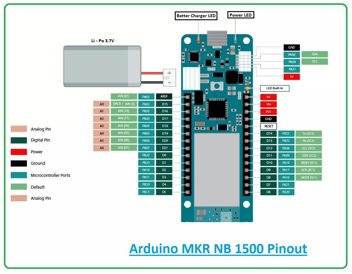
Hi Guys! Hope you’re well today. Happy to see you around. In this post today, I’ll walk you through the Introduction to Arduino MKR NB 1500. The Arduino MKR NB 1500 is mainly developed for working in remote areas where no power or internet connection is available. This board is based on a SAMD21 Cortex-M0+ 32bit low power microcontroller and comes with an operating voltage of 3.3V. Admit it. The Arduino board is a remarkable addition to the development of many automation and embedded projects. These boards are incorporated with a series of digital and analog pins that can be connected with the expansion boards or other breadboards. Most of the Arduino boards are integrated with 8-bit Atmel AVR microcontrollers. And all these boards incorporate different flash memory size to store the code. The two-way serial communication is added in the boards and some boards are given with the facility of the USB port that is used for the direct connection with the computer systems and to program and test the boards on the go. Arduino is an open-source platform that means you can edit and modify the hardware and software based on your requirements. The Arduino IDE software is used to program all kinds of Arduino boards. These boards are programmed using C and C++ language. I suggest you read this post all the way through, as I’ll walk you through the Introduction to Arduino MKR NB1500 covering datasheet, pinout, features, programming, pin description, and applications. Let’s jump right in.

Introduction to Arduino MKR NB 1500

  • The Arduino MKR NB 1500 is an Arduino board based on the SAMD21 Cortex-M0+ 32bit microcontroller that is mainly developed for applications in remote areas with no power or internet connection. On-field monitoring systems use these Arduino boards.
  • These are 22 digital I/O pins incorporated on the board. 7 analog and 12 PWM pins are also included in the chip.
  • The Rx and Tx pins are added to the board for the UART serial communication where Rx is used to receive the serial data and Tx is used to transmit the serial data.
  • Moreover, I2C and SPI communication protocols are also included in the device.
  • The power delivered to the board by USB is 5V. Plus, the board also incorporates a Li-Po charging circuit that makes the board run in two ways: either from the external 5V source or from battery power.
  • The clock speed of the oscillator is 32.768 kHz (RTC), 48 MHz which is required for the synchronization of the internal functions.
  • You can also interface the micro-sim with the board, however, micro-sim is not provided with the board. You need to purchase it separately.
  • You can interface breadboard with this board, giving you the ability to actually test and run your project on a breadboard before switching to the PCB design of the electrical circuit.
  • The board’s flash memory is 256KB. And it doesn’t incorporate EEPROM memory while the SRAM memory is 32KB.
  • The Arduino Program (sketch) is stored in the flash memory and SRAM memory is used to generate and manipulate variables when it runs.

Arduino MKR NB 1500 Datasheet

Before you apply this device to your electrical project it’s better to scan through the datasheet of the device that features the main characteristics of the board. You can download the datasheet of Arduino MKR NB 1500 by clicking the link below.

Arduino MKR NB 1500 Pinout

The following figure shows the pinout diagram of Arduino MKR NB 1500. There are three LEDs on the board. One is a built-in LED, and the other power LED and battery charger LED.

Arduino MKR NB 1500 Pin Configuration

Hope you’ve got a brief idea about this board. In this section, we’ll discuss the pin description of the pins incorporated on the board.

Digital I/O Pins

There are total 8 digital I/O pins integrated on the board which you can use as an input or output according to the requirements. They remain either HIGH or LOW. When they are HIGH they receive 5V and when they are LOW they receive 0V.

Analog Pins

There are total 7 analog pins incorporated on the board. As they are analog pins, they can get any number of values in opposed to Digital pins that only get two values i.e. HIGH or LOW

PWM Pins

The board comes with 12 PWM pins on board. When these pins are activated, the board generates analog result with digital means.

SPI Pins

This board incorporates SPI (serial peripheral interface) pins that are mainly employed to develop the communication between the controller and other peripheral devices such as sensors or shift registers. Two pins… MISO (Master Input Slave Output) and MOSI (Master Output Slave Input) are used for SPI communication. These pins are used to receive or send data by the controller.

I2C Pins

I2C is a two-wire communication protocol. That uses two lines i.e. SDA and SCL. The SDA is a serial data line mainly used to carry the data while SCL is a serial clock line mainly used for the synchronization of all data transfer through the I2C bus.

UART Pins

This device supports UART serial communication. Two pins Rx and Tx are used for the transmission and receiving of serial data.

Battery Connector

If you want to power up the board with the battery be sure to find the female 2 pin JST PHR2 Type connector. Polarity:  while you look at the board connector pins… Polarity is Left = Positive and Right = GND Vcc – This pin generates 3.3V using the on-board voltage regulator. 5V – This pin generates 5V when powered from the Vin pin of the board or from the USB connector. Vin – This pin provides power to the board using a regulated 5V source. If you supply power using this pin, the power through the USB port will be disconnected. This way you can power the board not using USB.

Arduino MKR NB 1500 Features

Microcontroller = SAMD21 Cortex®-M0+ 32bit low power ARM MCU Power Supply (USB/Vin) = 5V Operating voltage = 3.3V Digital I/O Pins = 22 Analog Pins = 7 PWM Pins = 12 I2C = 1 SPI = 1 UART = 1 DC current per I/O pin = 7mA EEPROM = no SRAM = 32KB Flash Memory = 256KB Supported Battery = Li-Po Single Cell, 3.7V, 1500mAh Minimum External Interrupts = 10 (0, 1, 4, 5, 6, 7, 8, 9, 16 / A1, 17 / A2) Size = 25 x 67 mm Weight = 32gr

Arduino MKR NB 1500 Programming

  • You can program this board using Arduino IDE (integrated development environment) software. This software is launched by Arduino.cc you can get this software by going to their site.
  • This board comes with a built-in Bootloader where you can burn the internal program, setting free from the hassle of burning and testing the program with the external burner.
  • This tiny device incorporates a USB port through which you can connect this device with the computer and run and test the program directly from the computer.

Arduino MKR NB 1500 Applications

This tiny little beast is used for a range of applications. Following are some major applications of this device.
  • Automatic Pill Dispenser
  • USB Joystick
  • USB Trackpad
  • Creating a wireless keyboard
  • Water Level Meter
  • Electric Bike
That’s all for today. I hope you’ve enjoyed reading this article. If you’re unsure or have any questions, you can pop your comment in the section below. I’d love to help you the best way I can. Feel free to share your valuable suggestions around the content we share so we keep producing quality content tailored to your exact needs and requirements. Thank you for reading the article.

AD623 Instrumentation Amplifier Datasheet, Pinout, Features & Applications

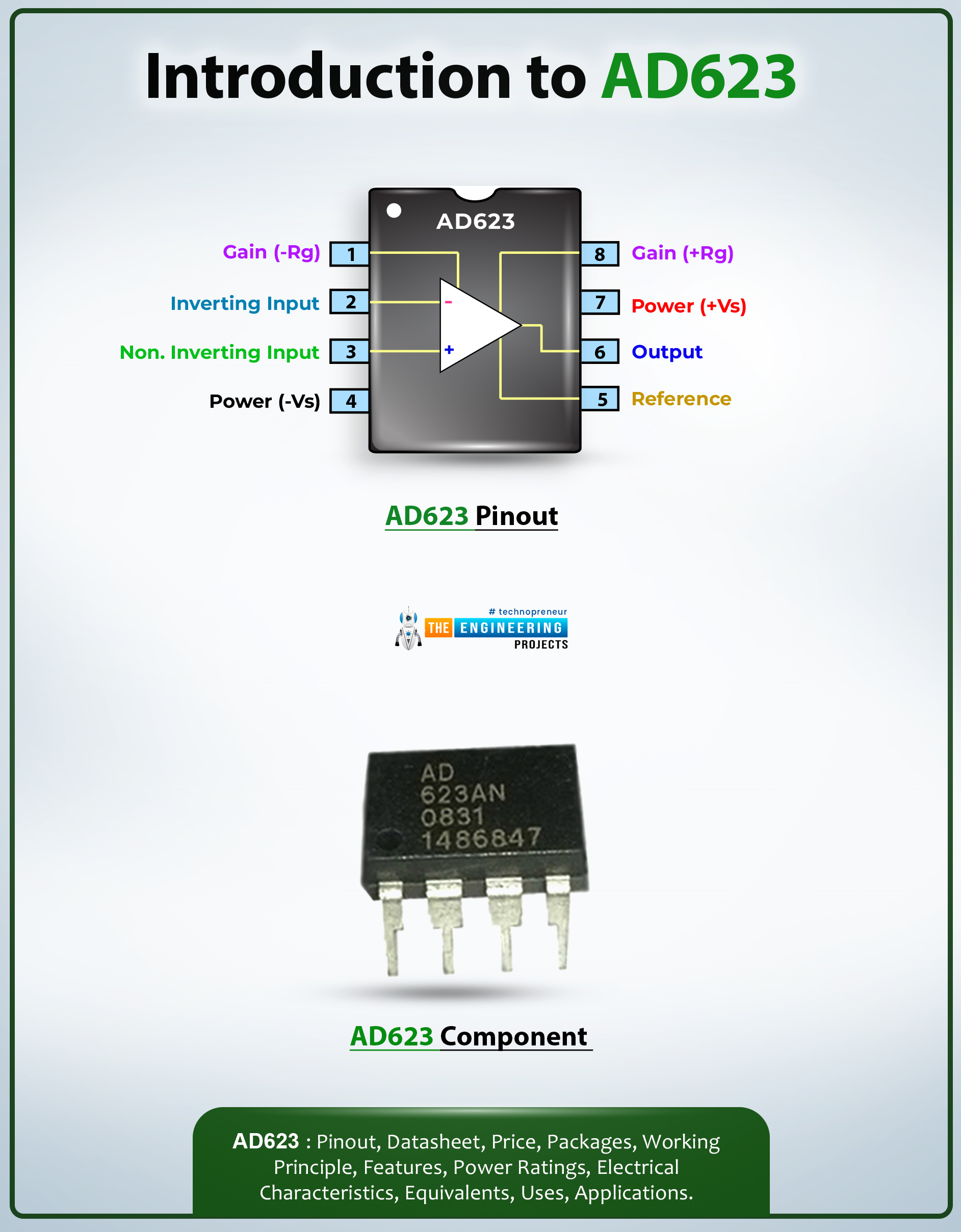
Hi Friends! I welcome you on board. Happy to see you around. In this post today, I’ll walk you through the Introduction to AD623.

The AD623 is an instrumentation amplifier integrated with a rail-to-rail feature. It is mainly used in battery-operated applications due to the low current of 500uA. It features a bandwidth of around 800 kHz which doesn’t require impedance matching since it incorporates buffer amplifiers that are attached to their input pins.

I suggest you buckle up as I’ll detail the complete Introduction to AD623 featuring datasheet, pinout, features, equivalents, and applications. Let’s jump right in.

Introduction to AD623

  • The AD623 is an instrumentation amplifier that falls under the category of differential amplifiers that incorporate buffer amplifiers attached to their input pins, making it a suitable pick for test and measurement equipment.
  • This device doesn’t require impedance matching which is a practice of making one impedance appear like another.

  • Rail-to-Rail feature is used in this amplifier which allows the output voltage to reach its full potential of positive rail voltage or negative rail voltage.
  • In a normal amplifier, this feature is not available as the output voltage of the amplifier is not equal to the supply voltage due to the presence of stage transistors which keep the amplifier from reaching its maximum positive or maximum negative voltage. Rail-to-Rail feature is used to overcome this problem.
  • Moreover, this device comes with very high input impedance, high common-mode rejection ratio, low noise, low drift, and low offset.
  • This kind of amplifier is mainly employed in the circuits where remarkable stability and accuracy is required.
  • Instrumentation amplifier is a type of differential amplifiers where the internal amplifiers are arranged in a way ­– one amplifier is used to generate desired output with enough impedance and the other amplifier is used to buffer each input (+,-)
  • Instrumentation amplifiers can be developed using standard individual amplifiers and precision resistors but also come in an integrated chip. This AD623 amplifier comes in an integrated chip that incorporates laser-trimmed resistors that provide a remarkable common-mode rejection ratio.

AD623 Datasheet

Before you incorporate this device into your electrical project, it’s wise to go through the datasheet of the component that features the main characteristics of the device. Click the link below to download the datasheet of AD623.

AD623 Pinout

The following figure shows the pinout diagram of AD623. The following table shows the pin description of each pin incorporated on the device.
Pin Description of AD623
Pin No. Pin Description Pin Name
1 Inverting Gain Terminal connected to a resistor to set gain value Gain (-Rg)
2 The Inverting input pin of the Op-Amp Inverting Input (IN-)
3 The Non - Inverting Input Pin of Amplifier Non- Inverting Input (IN-)
4 Negative supply terminal Power (-Vs)
5 Output reference input. Normally connected to common Reference
6 Amplifier output pin Output
7 Positive supply terminal Power (+Vs)
8 Non - Inverting Gain Terminal connected to resistor to set gain value Gain (+Rg)

AD623 Features

The following are the main features of AD623.
  • Gain Range = 1 to 1000
  • Set gain with only one resistor
  • Rail to Rail Instrumentation Amplifier
  • Bandwidth = 800KHz
  • Can operate on Single and Dual supply voltage
  • Operating current Max. = 550uA
  • Available Packages = 8-Pin PDIP, VSSOP and SOIC packages

AD623 Equivalents

The following are the alternatives to AD623.
  • JRC4558
  • LM4871
  • IC6283
  • AD620
Before you apply these alternatives to your project, it’s wise to double-check the pinout of the alternatives as it’s quite possible the pinout of the alternatives may differ from the pinout of the AD623.

AD623 Applications

The following are the main applications of AD623.
  • Employed in calibration and test equipment
  • Used in difference amplifiers
  • Used in the control system process
  • Employed in data Acquisition devices
  • Incorporated in low Power Medical instrumentation
  • Used in power-sensitive applications

That’s all for today. That was all about the Introduction to AD623. If you’re unsure or have any questions, you can pop your comments in the section below. I’d love to help you the best way I can. You’re most welcome to share your valuable feedback and suggestions around the content we share so we keep producing quality content customized to your exact needs and requirements. Thank you for reading the article.

Introduction to Arduino Pro Micro

Hi Folks! Hope you’re well today. Happy to see you around. In this post today, I’ll walk you through the Introduction to Arduino Pro Micro. Arduino Pro Micro is an Arduino compatible microcontroller board that is based on ATmega32u4. It operates at a frequency of 16MHz and 5V. It comes with 4 analog pins, 12 digital I/O pins, and 5 PWM pins. Moreover, it also supports serial communication UART with pins Rx and Tx. Arduino is an open-source platform provided by Arduino.cc that offers both hardware and software customization. Open-source means you can use, edit, or customize the board and software based on your requirements. Arduino boards are introduced in 2005 in Italy with the aim to provide a single platform where non-tech persons can get a hold of these boards and develop electronic devices that can interact with the environment using actuators and sensors. These boards are so easy to operate that even a common man with little knowledge about the boards can use them. These boards come in different sizes, memory space that you can incorporate in your electrical project. Not only can you program these boards, but you can also interface them with other shields and breadboard through digital I/O pins. Loading program from the personal computer is just one click away as some boards incorporate USB (universal serial bus) through which you can test and upload program directly from computers. This board is slightly different from the Arduino Micro board. The Arduino Pro Micro doesn’t include a reset button, 13 pin LED, and ICSP header and is smaller in size compared to the Arduino Micro board. I suggest you buckle up as in this tutorial I’ll detail the complete Introduction to Arduino Pro Micro covering pinout, pin description, features, communication and programming, and applications. Let’s jump right in.

Introduction to Arduino Pro Micro

  • Introduced by Sparkfun, Arduino Pro Micro is an Arduino compatible microcontroller board based on ATmega32u4.
  • This board operates at the frequency of 16 MHz which is required for the synchronization of the internal functions.
  • It comes with a built-in micro USB port that helps you test and program the Arduino board with a computer.
  • Though this tiny beast is small in size, it can perform functions like regular Arduino boards. This board comes with a flash memory of 32KB. And SRAM and EEPROM memories are 1KB and 2.5KB respectively.
  • The flash memory is the memory where the Arduino Program (sketch) is stored. While EEPROM memory is used to store long-term information and SRAM memory is used to produce and manipulate variables when it starts running.
  • In addition, this board is compatible with breadboards which makes it an ideal pick for a range of testing projects before you actually incorporate this device into your electrical project.
  • This board supports UART serial communication with two pins Rx and Tx. The former is the receive data line used to receive serial data while the latter is the transmission line used to transmit serial data.
  • The board incorporates resettable poly-fuse mainly employed to secure the USB port. It keeps the board from consuming too much power from the computer. When the current exceeds the given limit, the resistance of this polymeric material increases while it heats up. When the overcurrent is removed from the device, this fuse cools down and its resistance comes back to its original value.

Arduino Pro Micro Datasheet

Before you install this board into your electrical project, it’s wise to go through the datasheet of the board that contains the main characteristics of the board. Click the link below to download the datasheet of Arduino Pro Micro.

Arduino Pro Micro Features

The following are the main features of the Arduino Pro Micro board. CPU = 8bit Microcontroller = Atmega32u4 Digital I/O pins = 12 Oscillator = 16MHz USB = 1 ADC = 4x 10-bit ADC inputs PWM pins = 5 UART = 1 Reset button = no ICSP header = no Pin 13 LED = no Software Used = Arduino IDE Flash memory = 32KB EEPROM = 1KB SRAM  = 2.5KB Size = 34mm x 18mm

Arduino Pro Micro Pinout

The following figure shows the pinout diagram of Arduino Pro Micro.

Arduino Pro Micro Pin Description

Hope you’ve got the sneak peek of this Arduino board. In this section, we’ll detail the pin description of pins incorporated on the board.

Digital I/O Pins

There are 12 digital I/O pins available on the board that are either used as input or output based on the requirement. These pins are either OFF or ON. When they are ON they receive 5V and are considered as HIGH and when they are OFF they receive 0V and are considered LOW.

Analog Pins

This board incorporates 9 channels of 10-bit ADC. These are analog pins that receive any number of values in contrast to digital pins that get only two values i.e. HIGH and LOW.

PWM Pins

The Pro Micro board features 5 PWM channels which are used to get some of the analog output’s functions. When the PWM pins are triggered, the board creates analog results with digital means.

UART Pins

Moreover, it supports UART serial communication with two pins Rx and Tx. Both pins are used to transmit and receive serial data.

SPI Pins

This board comes with a serial peripheral interface (SPI) used to layout communication between the microcontroller and other peripheral devices such as and sensors shift registers. There are two pins for SPI communication i.e. MOSI (Master Output Slave Input) and MISO (Master Input Slave Output) – these pins are employed for sending and receiving the data by the microcontroller.

I2C Pins

  • Two pins are used for I2C communication which is a two-wire communication protocol. One is SDA and the other is SCL.
  • The former is a serial data line used to carry the data and the latter is a serial clock line used for the synchronization of all data transfer over the I2C bus.

Programming

  • The Arduino IDE (integrated development environment) software is used to program this Arduino board. This software is introduced by Arduino.cc which is used to program all kinds of Arduino boards.
  • This software is easy to use. As you install the software, you are given some basic LED blinking programs through which you can easily test the board on the go.
  • This tiny little beast contains a built-in Bootloader that is used to burn the program and it sets you free from the drill of compiling and burning the program from the external burner.
  • With a micro USB port, you don’t require a secondary processor as it appears to an attached computer as a keyboard and mouse. With this port, you can test and program the Arduino board directly from the computer.

Difference between Arduino Pro Micro and Arduino Micro

  • Through both boards incorporate Atmega32u4 microcontroller they differ in few features.
  • The Micro board comes with a reset button and ICSP header while the Pro micro board doesn’t incorporate those features.
  • Moreover, pro micro is smaller than micro board thus fewer pins are brought out to the Arduino terminal pins.
  • The missing pins include AREF, A4, A5, SS, 11, 12, and 13. This also projects that pin 13 doesn’t carry LED but it still supports Tx and Rx pins with LEDs for serial communication.
  • In addition, you cannot use the SPI interface in slave mode in the case of the Pro micro board as this board doesn’t bring out SS pin. And since the pro micro board cannot bring out AREF, the external ADC reference voltage ability is absent.
  • It is important to note that, though the board doesn’t carry ICSP connector, still it supports ICSP interface through which you can program the board.

Arduino Pro Micro Applications

The ability to easily groove in hard to reach places makes this board an ideal pick for a range of applications. This board can be used in the following projects.
  • Windows PC lock/unlock application
  • USB Trackpad
  • USB Joystick
  • Water Level Meter
  • Electric Bike
  • Creating a wireless keyboard
  • Automatic Pill Dispenser
That’s all for today. I hope you’ve got a clear idea about this Arduino Pro Micro board. If you have any questions, you can approach me in the section below. I’d love to help you the best way I can. Feel free to share your valuable feedback and suggestions around the content we share, so we keep producing quality content customized to your exact needs and requirements. Thank you for reading the article.

Introduction to Arduino USB Host Shields

Hello Everyone! Hope you’re well today. I welcome you on board. In this post today, I’ll walk you through the Introduction to Arduino USB Host Shields. With Arduino USB host shield you can interface the USB device to your Arduino board. This USB host shield is based on MAX3421E which is mainly known as the USB host controller that contains the analog circuitry and digital logic required to apply the USB full speed peripheral to USB specifications rev. 2.0. Moreover, this shield is compatible with TinkerKit which projects you can plug this TinkerKit module with the Arduino Boards.

Introduction to Arduino USB Host Shields

  • Arduino USB host shield is used to connect a USB device with the Arduino Board. Simply put, USB host shields provide the USB host capabilities to the Arduino boards.
  • With this USB host shield, you can connect any USB device with the Arduino boards.
  • What does this USB host mean? To understand this, you need to understand the USB protocol that comes with two types of devices. One is called the peripheral (client) and the other is called a host (server).
  • When the mouse or keyboard is attached to the computer through a USB port, your system acts as a host and the keyboard acts like a peripheral (client).
  • Successful communication is carried out using this USB protocol when one of the devices acts like a host which indicates you cannot attach two keyboards for the communication because both are peripheral devices.
  • The USB Host shield incorporates MAX3421E which is a separate chip that is mainly used to provide the USB host support to the Arduino board.
  • Once you connect this shield with the Arduino board, the board starts behaving like a host with you can attach other peripheral devices like a keyboard or mouse.
  • USB host shield is normally installed on the top of the Arduino boards.

Device Classes

The shield supports the following device classes.
  • Game controllers = Nintendo Wii, Sony PS3, Xbox360.
  • ADK-capable Android phones and tablets.
  • Bluetooth dongles.
  • USB to serial converters = FTDI, PL-2303, ACM, as well as certain cell phones and GPS receivers.
  • Mass storage devices: External hard drives, memory card readers, USB sticks.
  • Digital cameras: Powershot, Canon EOS, generic PTP, Nikon DSLRs and P&S
  • HID devices = keyboards, joysticks, mice, etc.

MAX3421E USB Peripheral/Host Controller with SPI Interface

  • Recall, MAX3421E chip known as the USB host controller that contains the analog circuitry and digital logic required to apply the USB full speed peripheral to USB specifications rev. 2.0.
  • This chip comes with a built-in transceiver that contains ±15kV ESD protection with programmable USB disconnect and connect.
  • SIE stands for (serial interface engine) which is mainly employed to control the low-level USB protocol details including bus retries and error checking.
  • The SPI interface can access the register set which is used to operate the chip and works at the frequency 26MHz.
The following figure shows the pinout diagram of the chip.
  • When MAX3421E operates as a host it provides a huge collection of USB peripherals to DSP, ASIC, and microprocessor.
  • The SPI interface operates at a voltage between 1.4V and 3.6V due to the internal level translators.
  • The MAX3421E comes in a 32-pin TQFN package (5mm x 5mm) and 32-pin TQFP package (5mm x 5mm) with operating temperature range from -40°C to +85°C

MAX3421E Datasheet

Before you apply any component to your electrical project, it’s wise to go through the datasheet of the component that contains the main characteristics of the device. Click the link below to download the datasheet of MAX3421E.

Applications

  • Embedded Systems
  • Microprocessors and DSPs
  • Medical Devices
  • Cameras
  • PDAs
  • Custom USB Devices
  • PLCs
  • MP3 Players
  • Set-Top Boxes
  • Instrumentation
  • Desktop Routers
That’s all for today. I hope you have enjoyed reading this article. If you’re unsure or have any questions you can approach me in the section below. You’re most welcome to share your valuable feedback and suggestions around the content we share so we keep producing quality content customized to your exact needs and requirements. Thank you for reading the article.

TDA1554 Audio Amplifier Datasheet, Pinout, Features & Applications

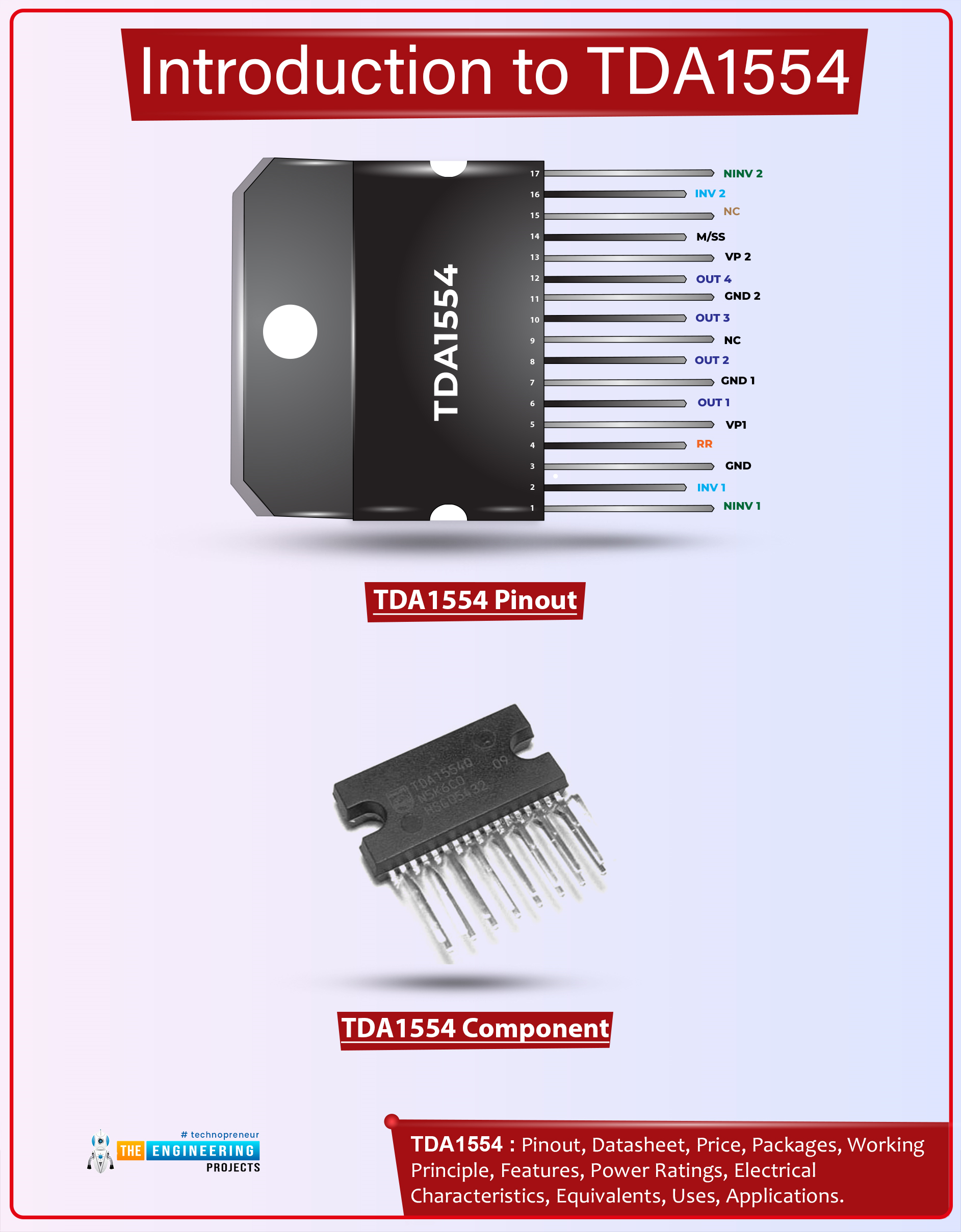
Hi Guys! Hope you’re well today. I welcome you on board. In this post today, I’ll walk you through the Introduction to TDA1554.

The TDA1554Q is an integrated class-B output amplifier mainly used for car radio applications. This device features 4 x 11 W single-ended or 2 x 22 W bridge amplifiers. It comes in a 17-lead single-in-line (SIL) plastic power package.

I suggest you buckle up and read this entire post till the end as I’ll discuss the complete Introduction to TDA1554 covering datasheet, pinout, features, and applications. Let’s get started.

Introduction to TDA1554

  • TDA1554 is a 4*11W single-ended or 2*22W power amplifier IC which means the internal circuitry features a 4*11W single-ended or 2*22W bridge amplifier.
  • It is an integrated class-B output amplifier that comes in a 17-lead single-in-line (SIL) plastic power package mainly used for car radio applications.

  • Out of four amplifiers incorporated in the device, two are non-inverting and two are inverting amplifiers.
  • Moreover, each amplifier comes with a gain of 20dB (26dB in BTL).
  • These amplifiers carry low thermal resistance and are thermally protected.
  • This device generates high output power and fixed gain.
  • Plus, a mute or standby switch is incorporated with the device helping you mute the amplifiers anytime you want.
  • This device can handle high energy on outputs and low voltage offsets at outputs and comes with good ripple rejection.

TDA1554 Datasheet

Before you apply this device to your electrical project, it’s better to scan through the datasheet of the component that features the main characteristics of the component. You can download the datasheet of TDA1554 by clicking the link below.

TDA1554 Pinout

The following figure shows the pinout diagram of TDA1554. The following table represents the pin configuration of each pin incorporated on TDA1554.
Pin Description of TDA1554
Pin No. Pin Description Pin Name
1 Non-inverting input 1 NINV1
2 Inverting input 1 INV1
3 Ground (signal) GND
4 Supply voltage ripple rejection RR
5 Positive Input Voltage 1 VP1
6 Output 1 OUT1
7 Power Ground 1 GND1
8 Output 2 OUT2
9 Not connected NC
10 Output 3 OUT3
11 Power Ground 2 GND2
12 Output 4 OUT4
13 Positive Input voltage 2 VP2
14 Mute/Stand-by switch M/SS
15 Not connected NC
16 Inverting input 2 INV2
17 Non-inverting input 2 NINV2

TDA1554 Features

  • Needs a few external components
  • Mute/standby switch
  • Remarkable ripple rejection
  • High output power and fixed gain
  • Flexibility in use - Quad single-ended or stereo BTL
  • Can handle high energy on outputs (VP = 0 V)
  • DC and AC short-circuit-safe to ground and VP
  • Low offset voltage at outputs (important for BTL)
  • Identical inputs (inverting and non-inverting)
  • Protected with Electrostatic Discharge, Load Dump, and Reverse Polarity
  • Low thermal resistance
  • Thermal protection

TDA1554 Power Ratings

  • Output Current = 4A
  • DC output offset voltage = 100mV
  • Supply Voltage Range = 6V to 18V
  • Input Impedance range = 50k? to75k?
  • Total Quiescent Current = 160mA
  • Stand-by Current = 10uA
  • Supply Voltage Rejection Ratio = 48dB

TDA1554 Applications

This component is mainly designed for car radio applications.

That’s for today. I hope you’ve enjoyed reading this article. If you have any questions, you can approach me in the section below. I’d love to help you according to the best of my expertise. Feel free to share your valuable feedback and suggestions around the content we share so we keep producing quality content tailored to your exact needs and requirements. Thank you for reading the article.

TDA2005 Amplifier Datasheet, Pinout, Features & Applications

Hi Everyone! Hope you’re well today. Happy to see you around. In this post today, I’ll walk you through the Introduction to TDA2005.

TDA2005 is a 20-watt Class B dual audio amplifier integrated chip. It comes in a Multiwatt11 package and is carefully designed for car radio applications. It can support the current up to 3.5A which is quite high which makes it a suitable pick for constructing power booster amplifiers.

I suggest you read this post all the way through as I’ll detail the complete Introduction to TDA2005 covering datasheet, pinout, features, and applications. Let’s jump right in.

Introduction to TDA2005

  • TDA2005 is a 20-watt Class B dual audio amplifier integrated chip. It is particularly designed for car radio applications.

  • It comes with a high current capability and features a total of 11 pins on board.
  • It supports low impedance loads of around 1.6 with an output power of more than 20 W.
  • TDA2005 features a bridge or stereo setup and the total power dissipation is 30W.
  • This device is mainly employed in applications where high-output audio power amplification is required.
  • Incorporated with protection against load dump voltage surge, this device features a maximum supply voltage of around +28V.
  • The repetitive current through each output is 3.5A while the maximum non-repetitive peak current through each output is 4.5A.
  • The storage temperature range is -40°C to 150°C while the operating temperature range is -23°C to 130°C.
  • This chip employed in stereo amplification applications will exhibit a voltage gain of 51 dB.

TDA2005 Datasheet

Before you apply this device to your electrical project, it’s wise to go through the datasheet of the component that features the main characteristics of the device. You can download the datasheet of TDA2005 by clicking the link mentioned below.

TDA2005 Pinout

The TDA2005 is an 11-pin device. The following figure represents the pinout diagram of TDA2005. The following table shows the pin name and pin description of TDA2005.
Pin Description of TDA2005
Pin No. Pin Description Pin Name
1 Non-Inverting Input of amplifier 1 INPUT+(1)
2 Inverting Input of amplifier 1 INPUT-(1)
3 Supply Voltage Rejection Ratio SVRR
4 Inverting Input of amplifier 2 INPUT-(2)
5 Non-Inverting Input of amplifier 2 INPUT+(2)
6 The ground is connected to this pin GND
7 Amplifier 2 bootstrap capacitor BOOTSTRAP(2)
8 The output of amplifier 2 OUTPUT(2)
9 Positive Power Supply +VS
10 The output of amplifier 1 OUTPUT(1)
11 Amplifier 1 bootstrap capacitor BOOTSTRAP(1)

TDA2005 Features

  • Overheat protection and output short circuit protection
  • A few components required to put the amplifier in working condition
  • Operating voltage range = +8 to +18V
  • High output power - Po=10 + 10 W @ RL = 2 ?, Po = 20 W @ RL = 4 ?
  • Programmable gain and bandwidth
  • Peak supply voltage = +40V for 50ms
  • Loudspeaker protection against short circuit
  • Incorporated with protection against load dump voltage surge
  • Supply voltage Max. = +28V
  • Comes with protection against fortuitous open ground
  • Total power dissipation = 30W
  • Comes with Bridge or Stereo setup
  • Repetitive current through each output = 3.5A
  • The non-repetitive peak current through each output Max. = 4.5A
  • Storage temperature range = -40°C  to 150°C
  • Operating temperature range = -23°C  to 130°C

TDA2005 Applications

The TDA2005 is used in the following applications.
  • Employed in Car radio
  • Used in Microphone amplifiers
  • Used in audio power amplifiers
  • Incorporated in Woofer amplifiers
  • Used in Music players

That’s all for today. Hope you found this article helpful. If you have any questions, you can pop your comment in the section below. I’d love to help you the best way I can. Feel free to share your valuable suggestions around the content we share so we keep creating quality content customized to your exact needs and requirements. Thank you for reading the article.

Introduction to Arduino Beetle

Hi Friends! Hope you’re well today. I welcome you on board. In this post today, I’ll walk you through the Introduction to Arduino Beetle. Arduino beetle is the smallest Arduino board that comes with the functionality of Arduino Leonardo. This board is a remarkable addition to the minimalistic Arduino technology. It is based on the microcontroller Atmel Atmega32u4. With the inception of innovations in modern technology, electronic devices are becoming light, more compact that happen to perform a lot of functions. These devices are economical and require little to no prior knowledge to get your hands dirty with them. All Arduino boards are microcontrollers but not all microcontrollers are Arduino board. While using the Arduino board, you don’t need to attach extra peripherals with the board, as it comes with built-in functions that don’t require the addition of external components. Earlier we have shared the articles on scores of Arduino boards including Arduino Uno, Arduino Leonardo, Arduino Due, and Arduino Mega. You can check these articles to find the basic information about them. I suggest you buckle up, as I’ll walk you through the complete introduction to Arduino Beetle covering datasheet, pinout, pin configuration, features, communication and programming and applications. Let’s jump right in.

Introduction to Arduino Beetle

  • Introduced by Arduino.cc, Arduino Beetle is the smallest Arduino Leonardo board that is based on Atmel Atmega32u4.
  • The Atmega32u4 is an 8-bit CMOS low power microcontroller
  • Arduino.cc offers an open-source platform for everyone which means you can optimize the boards and software programs as you like better.
  • The IDE (integrated development environment) is a software used to program the Arduino board. You don’t require prior knowledge and technical skills to start working with this board. The C and C++ are the languages used to program the Arduino beetle.
  • Though IDE software is compatible with MAC, Windows, or Linux Systems, Windows is a preferable operating system to use this board.
  • This tiny device comes with a micro USB port which means you can directly connect the device with the computer and program it based on your needs and requirements.
  • You don’t need a separate burner to burn and run the program on the board as it comes with a pre-burned Bootloader that allows you to upload the code in the hex file of the board.
  • The beetle is mainly introduced to provide the solution for low-cost disposable projects including DIY, gift projects, student projects, and e-textile.
  • This device operates at 5V and it also functions at 3.7V. Make sure voltage doesn’t exceed 5V else it can damage the device.
  • It comes with a clock time 16MHz. Several pins are incorporated on board out of which 10 are digital pins, 4 are PWM pins and 5 are analog pins.
  • This module comes with a crystal oscillator frequency up to 16 MHz that is mainly used to produce the clock pulses with decent speed. This oscillator is required for the synchronization of all the internal operations.
  • This module supports different communication protocols including I2C and UART.
  • The flash memory is 32KB out of which 4KB is used by the Bootloader. It is the memory where the sketch (the program we create on IDE is called a sketch) is stored.
  • The SRAM memory is 2.5KB which is the memory where sketch manipulates and produces variables when it operates. And EEPROM memory is 1KB and it is the space used for storing long-term information.
  • The price of this board at the time of writing this article is around 8$ which carries all powerful functions like Arduino Leonardo.

Arduino Beetle Datasheet

Before you incorporate this device into your electrical project, it’s wise to go through the datasheet of the device that features the main characteristics of the board. Click the link below to download the datasheet of Arduino beetle.

Arduino Beetle Features and Specifications

The following are the main features and specifications of Arduino beetle.
  • Board size 20mm x 22mm.
  • Direct testing and uploading program through a micro USB port.
  • I/O ports are V-shaped gold plated.
  • Two power interfaces that are gold plated and are used to supply power to the board.
  • Blue Light blink indicator which indicates the operation of the board.
  • Incorporated with Atmel Atmega32u4 microcontroller.
  • The operating voltage is 5V and the clock speed is 16MHz.
  • There are 5 analog pins, 4 PWM pins, and 10 digital pins on board.
  • Micro USB = 1
  • UART = 1
  • I2C = 1
  • EEPROM = 1KB
  • SRAM = 2.5 KB
  • Flash Memory = 32KB out of which 4KB is used by the Bootloader.
  • Write/Erase Cycles: 10,000 Flash/100,000 EEPROM
  • Data retention: 20 years at 85°C/ 100 years at 25°C

Arduino Beetle Pin Configuration

Still, reading? Perfect. I hope you’ve got a clear idea about this board. In this section, we’ll cover the pin description of the pins incorporated on the board.

Analog Pins

There are 5 analog pins incorporated on the board. These pins can receive any number of values in contrast to digital pins which receive only two values HIGH and LOW.

PWM Pins

This board doesn’t incorporate DAC (digital to analog converter) but it does incorporate 4 PWM pins which are used to get some of the analog output’s functions. During this PWM (pulse width modulation) process, the board generates analog results with digital means.

Digital Pins

There are total 10 digital pins incorporated on board. These pins are developed to be configured as outputs or inputs based on the requirement. These pins are either ON or OFF. When they are ON they are in HIGH voltage state getting 5V and when they are OFF they are in LOW voltage state getting 0V.

Atmega32u4 Pinout

The following figure shows the pinout diagram of Atmega32u4.

Atmega32u4 Pin Description

In this section, we’ll cover the pin description of each pin incorporated on Atmega32u4.

Vcc

It is a digital voltage supply pin.

GND

This pin is connected to the ground.

Port B (PB7...PB0)

Port B is an 8-bit bidirectional I/O port that is incorporated with pull-up resistors. These resistors are used to limit the current and prevent it exceeding from a certain number. This port comes with efficient driving capabilities compared to other ports. When this port is used as an input, this will source current due to the port pins that are extremely pulled low. This happens when the pull-up resistors are activated.

Port C (PC6, PC7)

Port C is similar to Port B - an 8-bit bidirectional I/O port incorporated with pull-up resistors. When the pull up resistors are activated, Port C will source current with port pins extremely pulled low.

Port D (PD7..PD0)

Port D is an 8-bit bidirectional I/O port that comes with pull-up resistors. When the reset condition meets, the Port D pins are tri-stated.

Port E (PE6, PE2)

Only two bits... PE6 and PE2 are present on the device pinout. It is an 8-bit bidirectional port incorporated with internal pull-up resistors.

Port F (PF7..PF4, PF1,PF0)

Port F is a bidirectional port that acts like analog inputs to the A/D converter. Two bits PF2 and PF3 are not present on the product pinout.

D-

USB Full speed / Low Speed Negative Data Upstream Port. It should be attached to the USB D- connector pin along with the serial resistor 22W.

D+

USB Full speed / Low Speed Positive Data Upstream Port. It is connected to the USB D+ connector pin along with the serial resistor 22W.

UGND

USB pads ground.

UVCC

Regulator Input supply voltage applied to USB pads.

UCAP

Internal Regulator Output supply voltage applied to USB pads.

VBUS

USB VBUS monitor input.

RESET

This is a reset pin. A low level applied to this pin for a longer time will produce a reset. Shorter pulses may not generate a reset.

XTAL1

Input to the internal clock operating circuit and Input to the inverting Oscillator amplifier.

XTAL2

Output from the inverting Oscillator amplifier.

AREF

This is used as the analog reference pin for the A/D Converter.

AVCC

AVCC is the supply voltage pin for all the A/D Converter channels.

Communication and Programming

  • Recall, this module supports different communication protocols i.e. I2C, and UART.
  • The I2C is a two-wire communication protocol that carries two main lines called SCL and SDA. The former is a serial clock line required for the synchronization of all data transfer over the I2C bus. While the latter is a serial data line mainly employed to carry the data.
  • And the UART is mainly used for serial communication and comes with two lines Tx and Rx where the former is used to transfer the serial data and the latter is used to receive the serial data.
Arduino IDE software is used to program all types of Arduino Boards. Attach micro USB to the Beetle and select Arduino Leonardo from your board type on the Arduino IDE software.

Arduino Beetle Applications

This tiny little beast is a full system in a small package as it incorporates almost all functions like Arduino Leonardo. The following are some applications of Arduino Beetle.
  • Health and security systems
  • Creating a wireless keyboard
  • Industrial automation
  • Embedded systems
  • Student projects
  • Automatic pill dispenser
  • Water level meter.
You’ll find a lot of microcontrollers in the market that are more economical than the Arduino board. But still, most of the hobbyists and students prefer Arduino Board over microcontroller. The reason is clear. Arduino board comes with a big community that shares expertise and knowledge for a wide range of audiences. Help is readily available that you’ll never find in the case of microcontrollers. Moreover, when you select Arduino board over microcontroller, you don’t need additional components and extra peripherals to connect with the board, as this board comes with a lot of built-in functions, setting you free from the hassle of connecting a lot of components. Simply, you need to plug the device with the computer and play with it on the fly. That’s all for today. I hope you’ve enjoyed reading this article. If you’re unsure or have any questions, you can pop your comment in the section below, I’d love to help you the best way I can. Feel free to share your valuable suggestions and feedback around the content we share so we keep coming up with quality content customized to your exact needs and requirements. Thank you for reading the article.

LM747 Datasheet, Pinout, Features, Equivalent & Applications

Hi Guys! I hope you’re well today. Happy to see you around. In this post today, I’ll walk you through the Introduction to LM747.

LM747 is a general-purpose dual-operational amplifier IC. This chip contains two operational amplifiers on board and belongs to the LM’xx’ family where LM stands for linear monolithic. In this chip, analog components are incorporated into silicon.

I suggest you buckle up as I’ll detail the complete Introduction to LM747 covering datasheet, pinout, features, equivalents, and applications. Let’s jump right in.

Introduction to LM747

  • Designed by National Semiconductor, LM747 is a general-purpose dual-operational amplifier integrated chip.
  • Two operational amplifiers are incorporated that share common power supply leads and a bias network.

  • And these amplifiers are capable of performing two different operations at the same time which makes them a suitable pick for several applications. Though these amplifiers share a common bias network, they are completely independent of each other
  • As two general-purpose amplifiers are used in this chip, it is used to construct op-amp circuits like differential amplification, comparator, and mathematical operations.
  • This device features offset pins which are mainly used to make the output more accurate and efficient.
  • It comes with no latch-up when the input common-mode range is exceeded which sets it free from oscillations.

LM747 Datasheet

Before you incorporate this device into your electrical project, it’s better to scan through the datasheet of the component that features the main characteristics of the component. You can download the datasheet of LM747 from the link given below.

LM747 Pinout

LM747 incorporates 14 pins on board. The following figure shows the pinout diagram of LM747. The following table details the pin name and pin description of each pin on LM747.
Pin Description of JRC4558
Pin No. Pin Description Pin Name
1 Inverting input of op-amp 1 1IN-
2 A non-inverting input of op-amp 1 1IN+
3 The offset null pin is used to remove the offset voltage and control the input voltages for op-amp 1 OFFSET  NULL 1
4 Common negative supply voltage for both Op-amps V-
5 The offset null pin is used to remove the offset voltage and control the input voltages for op-amp 1 OFFSET  NULL 2
6 The non-inverting input of op-amp 2 2IN+
7 Inverting  input of op-amp 2 2IN-
8 The offset null pin is used to remove the offset voltage and control the input voltages for the op-amp 2 OFFSET  NULL 2
9 Positive supply voltage for op-amp 2 V2+
10 The output pin of the op-amp 2 2OUT
11 No connection NC
12 The output pin of the op-amp 1 1OUT
13 Positive supply voltage for op-amp1 V1+
14  The offset null pin is used to remove the offset voltage and control the input voltages for op-amp 1 OFFSET  NULL 1
  • Offset null pins remove the offset voltage and balance the output voltages for both operational amplifiers.
  • While pin 11 is not connected. It is not used for any purpose.

LM747 Features

The following are the main features of LM747.
  • No latch-up
  • Large differential voltage and common mode range
  • Low noise interference among op-amps
  • Total power dissipation = 800mW
  • Differential input voltage = ±30V
  • Low power consumption
  • Supply voltage Max. = ±22V
  • Frequency Compensation is not required
  • Comes with short-circuit protection
  • Common-Mode Rejection Ratio CMRR = 90dB
  • Operating temperature range = -55ºC to +125ºC

LM747 Applications

The following are the main applications of LM747.
  • Employed in mathematical operations
  • Used in amplifiers
  • Used in analog circuits
  • Used for Measuring instruments
  • Incorporated in voltage comparators
  • Employed for Industrial applications
  • Used in Peak detectors

That was all about the Introduction to LM747. If you’re unsure or have any questions, you can leave your query in the section below. I’d love to help you according to the best of my expertise. Feel free to share your valuable feedback and suggestions around the content we share so we keep sharing quality content tailored to your exact needs and requirements. Thank you for reading the article.

Syed Zain Nasir

I am Syed Zain Nasir, the founder of <a href=https://www.TheEngineeringProjects.com/>The Engineering Projects</a> (TEP). I am a programmer since 2009 before that I just search things, make small projects and now I am sharing my knowledge through this platform.I also work as a freelancer and did many projects related to programming and electrical circuitry. <a href=https://plus.google.com/+SyedZainNasir/>My Google Profile+</a>

Share
Published by
Syed Zain Nasir