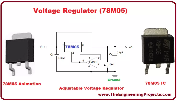
Hello everyone! I hope you will absolutely fine and having fun. Today, I am going to give you a detailed discussion on the topic Introduction to 78M05. I have already shared information about different IC's e.g. Introduction to UA741, MMBD914, LM224, LM386 and LM317. You must have a look at all these tutorials for the better understanding of this article. 78-M05 is basically a three (3) terminal. These terminals include input, output and the common terminal.
78-M05 is commonly available in TO-220 package having different fixed voltages at the output. Its construction process is based on planar epitaxial technology. These regulators are used for the employment of the process of internal limitation of the current. Safe area compensation as well a ...
Hello friends! I hope you all will be absolutely fine and having fun. Today, I am going to give you an elaboration on Introduction to 2N3772. I have already shared basic knowledge about different IC's and transistors in my previous tutorials e.g. Introduction to IRF540, BC547, MMBD914, LM339, LM224 and LM386. You must have alook at these tutorials before going into the details of this tutorials. It will be quite helpful in the better understanding of this article. 2N-3772 is basically a type of central semiconductor. It is basically a Negative Positive Negative (NPN) semiconductor. This semiconductor is designed by the process named as epitiaxial process. The main purpose behind its designing is to provide the high power based amplification proce ...
Hello friends! I hope you all will be absolutely fine and having fun. Today, I am going to give you an elaboration on Introduction to 2SC3320. I have shared the basic knowledge of different electronic devices in my previous articles like Introduction to ULN2003, LM317, LM393, IRF540, BC547, UA741 and MC34063. 2SC-3320 is a Negative Positive Negative (NPN) transistor. It is made up of silicon. It is basically a power transistor. Power transistor is an electronic device which is able to handle certain level of power. 2SC-3320 has three terminals whose detail will be given later. Its an efficient device with higher efficiency available at at lower cost in the market these days. Due to cost efficiency and its unique features it is more popular devic ...
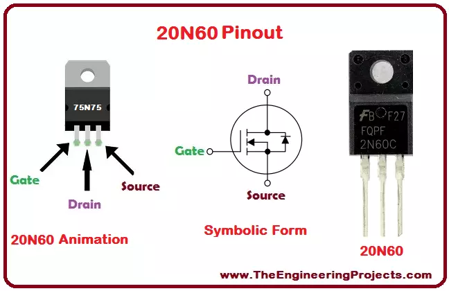
Hello friends! I hope you all will be absolutely fine and having fun. Today, I am going to give you an elaboration on Introduction to 20N60. 20-N-60 is basically a power Metal Oxide Semiconductor Field Effect Transistor (MOSFET). Power MOSFET is a device that can handle a specific level of power. I have already shared information about MOSFET in my previous tutorials e.g. Introduction to 75N75, SG3524, 50N06, IRFZ44N, C945 and TL072. Before going into the details of this article you must have a look at these articles. They will result in the better understanding of this article.
MOSFET family is divided into two categories. P-channel MOSFET and N-channel MOSFET. 20-N-60 belongs to the N-channel MOSFET. It is based on United Technologies Corporat ...
Hello friends! I hope you will be absolutely fine and having fun. Today, I am going to give you an elaboration about Introduction to 50N06. 50-N-06 is a device having three terminals named as gate, drain and source respectively. It is made up of silicon and is capable of current conduction up to 50A. I have already shared basic knowledge about different electronic devices in my previous articles like Introduction to MC34063, MMBD914, MSP430, NE555, NE556 and LM2902. Before going into the details of this article you must go through my previous tutorials for the better understanding.
50-N-06 provides fast switching speed. 50N06 is an N-channel power Metal Oxide Field Effect Transistor (MOSFET) specially designed to handle particular power levels. ...
Hello friends! I hope you will be absolutely fine and having fun. Today, I will give you an elaboration on Introduction to SG3524. I have already shared articles on Introduction to 74HC245, 74HC595, CD4051, L293D, L298, LF351 and LF411. You should also go through all of these tutorials in order to have a better understanding. SG 3524 consists of all the important functions necessary to design inverters.
Moreover, using SG-3524 we can also design regulation power supplies as well as switching regulators. This all design is based on a single chip. High power applications can also be controlled through this device. SG-3524 is especially designed for voltage doublers without transformers, transformer coupled DC to DC converters. Their design was als ...
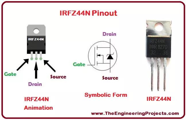
Hello everyone! I hope you all will be absolutely fine and having fun. Today, I am going to provide you a detailed Introduction to IRFZ44N.
IRFZ44N belongs to the family of Metal Oxide Semiconductor Field Effect Transistor (MOSFET). It is a power MOSFET. There are two types of MOSFET i.e. N-channel and P-channel. IRF-Z44N belongs to the N-channel family. It uses "Trench" technology and is enveloped in a plastic structure. It has very low on state resistance. It has zener diode, which provides ESD protection up to 2 kilo-volt. It is a low cost device and provides higher efficiency. It is easily available in the market these days and is mostly known because of its vast applications. IRF-Z44N has modern features i.e. advance processing technology, ...
Hello friends! I hope you will be absolutely fine and having fun. Today, I will give you a detailed discussion about Introduction to 75N75. I have also shared different articles on Introduction to 2N3904, 2N3906, BC547, C945 and IRF540. You must go through all of these articles for the better understanding of this tutorial. 75-N75 is basically a Metal Oxide Field Effect Transistor (MOSFET). MOSFET is a transistor which is frequently used in electronic devices for the amplification and fast switching purposes.
MOSFET consists of four different terminals. These terminals include body terminal, source, drain and gain respectively. There two different type of transistors i.e. P-channel transistor and N-channel transistor. 75N-75 is N-channel MOSFET. ...
Hello everyone! I hope you all will be absolutely fine and having fun. Today, I would like to provide a complete discussion on Introduction to C945. You will see a detailed description on the basics of the transistor C-945 and its different parameters. I have already shared Introduction to MMBD914, 74HC245, NE556, LM348 and PIC18F4550. So, must go through these tutorials in order to have better understanding about different IC's. C-945 transistor is basically a Negative Positive Negative (NPN) bipolar junction transistor.
C945 is usually used in the electronic circuits where there is a need of high speed transistor and a low current. C-945 has three semiconductor regions named as emitter, base and collector respectively. Since C-945 is a bipolar ...
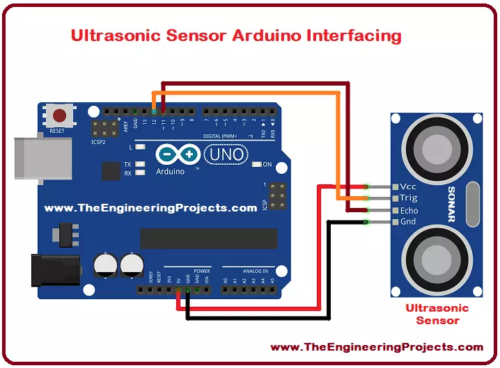
Hello everyone! I hope you all will be absolutely fine and having fun. Today, I would like to provide a complete discussion on Ultrasonic Sensor Arduino Interfacing. I would like to tell you some detail about ultrasonic sensor, after that we will move towards ultrasonic sensor Arduino interfacing. Ultrasonic sensor is also known as SONAR sensor. SONAR basically stands for Sound Navigation and Ranging. Ultrasonic is mostly used for the distance measurements. It can also be used for measuring the depth of the sea.
I have already shared Ultrasonic Sensor Library for Proteus. Ultrasonic/SONAR sensor is an electronic device used to estimate the distance of an object by continuously transmitting sound waves at a particular frequency and listens to tha ...