Introduction to 1n914

Hello Everyone! I always love to keep your stomach filled with useful information so you can excel and grow in your relevant field. Today, I am going to reveal the details on the Introduction to 1n914. It is a small signal diode that allows the current to flow in one direction and blocks the current in other direction. It features operating junction temperature of 175 ºC and forward surge current of 4A. It is widely used for industrial and power management applications. I'll give you a brief details about this diode, so you don't have to go anywhere else for finding the information regarding this small signal diode. Let's get started.

Introduction to 1n914

  • 1n914 is a small signal diode that is widely used in portable devices.
  • It exhibits zero resistance in one direction and maximum resistance on the other direction, so current will flow in one direction only.
  • This unidirectional behavior is sometimes referred as a rectification which is an ability to convert AC current to DC current.
  • This diode is also termed as a electronic version of check valve.
  • It is basically a polarized components which consists of two terminals called anode and cathode.
  • Normally silver mark shows the cathode side of the diode.
  • It will only conduct when there is some form of threshold voltage present in its forward biased mode.
  • It will seize the current to flow in reverse biased mode.
  • Normally diode exhibit non linear current-voltage characteristics, however these non-linear characteristics can be customized by using a specific semiconductor and doping impurities that are diffused in the diode material during the manufacturing process of diode.
  • These diodes are widely used for power conversion. Rectifiers are made from diodes which convert AC current to DC current and provide better performance.
  •  Diodes are used to protect highly sensitive electronic devices from voltage surge. In normal conditions, these diodes are reverse biased and don't conduct. When there is any surge of high voltage occurs, current starts to flowing and they get forward biased.
  • Many integrated circuits are incorporated with these diodes which block the high voltage surge and save the sensitive transistors from damaging.
Properties
  • This diode features forward surge current of 4A at pulse width 1µs.
  • It shows 1A surge current at pulse width of 1s.
  • Operating junction temperature of 175 C.
  • Maximum repetitive reverse voltage of 100V.
  • Maximum power it can dissipate is 500mW.
  • Forward voltage of 1V at 10mA.
  • Reverse recovery time of 4ns.
Features
  • It shows high conductance in one direction only. It blocks the current in other direction.
  • This signal diode is highly reliable and come with low cost.
  • Fast switching speed makes the function of this diode incredibly simple.
  • Used for general purpose switching applications.
  • It is AEC-Q101 qualified and highly durable.
Absolute Maximum Ratings
Following figure shows the absolute maximum rating of 1n914 small signal diode.
  • It is important to note that if stresses are exceeded above absolute maximum ratings, they can damage the device.
  • Similarly if stresses are applied for extended period of time, they can effect the device reliability.
  • These absolute maximum ratings are the limiting values above which the diode serviceability may be affected.
Applications
  • It is widely used in industrial applications.
  • Power management and portable devices use this type of diode.
  • It is useful for the demodulation of AM (amplitude modulated) radio signal. Actually AM signal mainly contains alternately positive and negative peaks of the carrier wave. The amplitude of these signal is directly proportional to original audio signal. Function of diode is to rectify the AM signal which ultimately leaves behind the original positive cycles of the carrier waves. Filter is used to extract the audio signal from this rectified carrier wave and then fed into the amplifier that produces sound waves.
  • Diodes are incorporated with other components to make AND and OR logic gates.
  • These diodes are widely used as a temperature sensing device because forward voltage drop is highly dependent on temperature.
That's all for today. I hope you have enjoyed the article. For your convenience, I always try to give information in sorted form so you can digest the information without much effort. However, if still you feel skeptical or have any question about understanding the concept of this diode, I'd love to help you in this regard according to best of my expertise. Your suggestions and feedback will be highly appreciated. Stay Tuned!

Introduction to 2n3053

Hey Guys! I hope you are doing great and having fun. Today, I am going to give you the details on the Introduction to 2n3053. It is an NPN bipolar junction transistor which is mainly designed for amplification and switching applications. It consists of P doped semiconductor that exists between the two N doped layers. I'll give you a brief details about this transistor so you don't have to go anywhere to finding information regarding this transistor. Let's get started.

Introduction to 2n3053

  • 2n3053 is an NPN bipolar junction transistor which is mainly used for general purpose amplification and switching purpose.
  • It consists of three terminals called emitter, base, and collector. and comes in TO-39 Metal Can Package.
  • This NPN transistor exhibits low leakage current, high breakdown voltage and low capacity and beta value which are useful over a wide range of current.
  • As it is an NPN transistor, so base will be positive with respect to emitter.
  • Sometimes it is called current controlled device because small current at the base side is used to control large current at the emitter and collector side.
  • It is called BJT(bipolar junction transistor) because conduction is done by the movement of both electrons and holes but majority charge carriers will be electrons.
  • When we apply positive voltage at the base side, it gets biased and then it handles the current at the emitter and collector side.
  • The ability of base to control number of electrons is used for amplification purpose.
  • P terminal of the transistor is behaved like base and other two N terminals represent emitter and collector respectively.
  • The emitter emits the electrons which are then controlled by base and collected by collector.
2n3053 Pinout
2n3053 is an NPN transistor which mainly consists of three terminals. 1: Emitter 2: Base 3: Collector
  • Transistor action is triggered by the free movement of electrons from its base side.
  • These free electrons act like a bridge between emitter and collector.
Circuit Diagram of 2n3053
The Circuit diagram of 2n3053 is shown in the figure below.
  • In order to flow current from emitter to collector, base voltage must be positive with respect to emitter.
  • The current at the emitter side is the sum of current at the base and collector side.
  • Forward current gain is the ratio between collector current to base current and it is denoted by beta ß. Beta is a ratio between two current so it has no unit.
  • This beta value is sometimes referred as an amplification factor i.e. it is used for amplification purpose.
  • Beta value ranges between 20 and 1000 but standard value of beta is 200.
  • Current gain of the transistor is represented by alpha a. It is a ratio between collector current and emitter current. Alpha value exists between 0.95 to 0.99 but most of the time alpha value is considered as unity.
Absolute Maximum Ratings of 2n3053
  • Absolute maximum rating of 2n3053 is shown in the figure below.
  • Collector-Base and Collector-Emitter voltages are 60V and 40V respectively.
  • The maximum power it can dissipate is 5W.
  • It is important to note that if stresses are exceeded from given absolute maximum ratings, they can damage the device.
  • Also, if stresses are applied for extended period of time, they can effect the device overall reliability.
  • This bipolar junction transistor mainly consists of silicon semiconductor that's the reason it is mostly referred as Switching Silicon Bipolar Transistor.
Main Difference between NPN and PNP transistors
  • Main difference between NPN and PNP transistors are the charge carriers.
  • In case of NPN transistor majority charge carriers are electrons while majority charge carriers are holes in case of PNP transistors.
  • Most of the professional prefer NPN transistors over PNP transistors, because conduction through mobility of electron is better than mobility of holes.
Applications
  • This transistor is mainly used for general purpose amplification.
  • It is widely used as a simple switch. Actually, conduction starts between emitter and collector when voltage is applied at the base side. When there is no bias voltage at the base side, the switch will be OFF. If voltage is present at the base side, switch will be ON.
That's all for today. I try my best to give information sorted out in easy and small steps so you can easily digest the information without much effort. If you have any doubt or feeling skeptical about the working of this transistor you can ask me in the comment section below. I'll try my best to help you according to best of my expertise. We always love when you keep coming back for what we have to offer. Stay tuned!

Introduction to 2n2646

Hey Fellas! I always come with unique topics to whet your appetite with valuable information so you can excel in your relevant field. Today, I am going to unlock the details on the Introduction to 2n2646. It is a uni-junction transistor which is mainly used in thyristor triggering circuits, sensing circuits, and pulse and timing circuits. It features low peak point current of about 5µA, and low emitter reverse current of 0.005µA and passivated surface for uniformity. Let's dive in the details of this transistor and explore what it does and what are its main applications? Let's get started.

Introduction to 2n2646

  • 2n2646 is a three terminal semiconductor device that contains only one junction that behaves like an electrically controlled switch.
  • This uni-junction transistor (UJT) can not be used as a linear amplifier but it is widely used in triggered oscillators, free-running oscillators, and pulse generation circuits of low frequencies.
  • It is composed of n-type semiconductors where p-type material is embedded along its length that helps in fixing the parameter like intrinsic stand off ratio which can be denoted as ?.
  • Typical uni-junction 2n2646 contains three terminals named as emitter(E), base 1(B1) and base 2(B2).
  • Sometimes it is also referred as a double base diode.
  • The base is composed of lightly doped n-type silicon. The emitter is heavily doped and contains p-type material.
  • The name of the device is based on the single junction formed between n-type and p-type material.
  • When the emitter is behaved as open-circuit, the resistance between B1 and B2 is called inter-base resistance.
  • The emitter junction is closed to B2 than B1, so this device doesn't encompass a symmetrical structure.
  • Only a fraction of current will flow from B1 to B2 when there is no potential difference between emitter and base terminals.
  • However, if large voltage is applied at the emitter terminals then a very large current will flow from B1 to B2 which ultimately generates larger B2 output current.
  • The structure of this UJT is quite similar to N-Type JFET, but the gate surface in N-Type JFET is much larger than the emitter junction in UJT.
  • This UJT normally functions when emitter junction is forward biased while JFET normally functions when gate junction is reversed biased.
  • It is also referred as a current controlled with negative resistance.
2n2646 Pinout
2n2646 is mainly composed of three terminals. 1: Emitter 2: Base1 (B1) 3: Base2 (B2)
  • This 2n2646 is designed for industrial applications where circuit economy is taken into consideration.
  • It is an ideal choice for firing circuits that are widely used in silicon controlled rectifiers.
Working of 2n2646
  • When this device is triggered it allows the emitter current to increase until it is limited by the help of emitter power supply.
  • It can be used as an oscillator because it exhibits a negative resistance.
  • This UJT gets biased when positive voltage is applied between the two bases. It will cause a potential drop in the device.
  • The current will start to flow from emitter to base region, when emitter voltage is exceeded one diode voltage above the voltage where diffusion of P-type material occurs.
  • This additional current at the base region allows the resistance between emitter and B2 lead to decrease, hence overall improves the conductivity of the device.
  • This resistance drop will make the emitter junction forward biased which helps in injecting the more current.
  • This drop in resistance makes the device operate over negative resistance that's why it is useful for oscillator circuits.
Absolute Maximum Ratings
Absolute maximum ratings of 2n2646 is shown in the figure below.
  • Stresses above than the given values can damage the device.
  • Also if stresses are applied for extended period of time above normal operating values, they can effect the device reliability.
Electrical Characteristics
Electrical characteristics of 2n2646 are shown in the figure below.
  • It is important to note that these electrical characteristics don't effect the performance of the transistor.
  • The 2n2646 is mainly manufactured for the purpose where low peak point emitter current, and low emitter leakage current is required.
Applications
  • 2n2646 is mainly used in pulse and timing circuits.
  • It is a building block of thyristor triggering and sensing circuits.
  • Free-running oscillators and pulse generation circuits with low frequencies use this UJT because it exhibits negative resistance.
That's all for today. I always try to sort out information into small steps so you can digest the information easily. I hope you have enjoyed the article and got a clear idea what this UJT does and what are its main applications? However, if still you feel skeptical or have any doubt you can ask me in the comment section below. I'll help you according to best of my expertise. Stay Tuned!

Introduction to 2n4403

Hi Everyone! I hope you are doing great and enjoying your life. I am back to give you daily dose of information so you can grow and progress in your relevant field. Today, I am going to give you the details on the Introduction to 2n4403. It is basically PNP(Positive-negative-Positive) bipolar junction transistor where N doped layer is sandwiched between the two P doped layers. It comes in plastic TO-92 compact casing. I'll try to give you brief details about this transistor so you don't need to go anywhere for finding the information regarding this transistor. Let's get started.

Introduction to 2n4403

  • 2n4403 is a PNP bipolar junction transistor where conduction is carried out by the movement of holes and electrons but majority charge carriers will be holes.
  • It consists of three terminals named as emitter base collector. N layer represents the base of the transistor while other two layers represent emitter and collector respectively.
  • It works similar to NPN transistor where small amount of current at the base side is used to control the large current at the emitter and collector side.
  • As it is a PNP transistor so base terminal will be negative with respect to emitter.
  • Most of the transistors behave like a switch because when we apply small voltage at the base side, it is used to control the large current at the emitter and collector side and switch will be considered ON.
  • When there is no bias at the base side the switch is considered OFF.
  • PNP transistors also known as current controlled device because small current at the base side is used to control the large current at the emitter and collector side.
2n4403 Pinout
2n4403 is a bipolar junction transistor which consists of three terminals. 1: Emitter 2: Base 3: Collector
  • The small current that leaves the base will be amplified at the collector output.
  • This PNP transistor will only conduct if base is negative with respect to emitter terminal.
2n4403 Circuit Symbol
Circuit symbol of 2n4403 is shown in the figure below.
  • PNP transistor can be considered normally OFF, but negative voltage at the base side and small out put current can turn it ON and helps in flowing large emitter-collector current.
  • PNP will only conduct when voltage at the collector side Vc is much smaller than voltage at the emitter side Ve.
  • Current at the emitter side is the sum of current at the base and collector side.
Absolute Maximum Ratings of 2n4403
Absolute maximum ratings of 2n4403 is shown in the figure below.
  • It is important to note that if stresses are exceeded from absolute maximum ratings, they can damage the device.
  • Similarly if stresses are applied for extended period of time above the normal operating condition, they can effect the device reliability.
Transistor as a Matched Switch
  • In most of the cases PNP transistors widely replace NPN transistors and they can also be used as a switch.
  • You may come across a question what do we use PNP transistors while NPN can be widely used for switching and amplification purpose. However, when we combine these two different types of transistors, they come with a lots of advantages.
  • Class-B amplifiers are incorporated with two pairs of PNP and NPN transistors, where both transistors are used to control the direction of current flowing in both directions at any time.
  • Transistors are termed as “Complementary Transistors” which use both NPN and PNP transistor of identical characteristics.
  • Both transistors, in Class B-amplifiers,  work in a similar way i.e. PNP transistor conducts for the negative half cycle of the transistor while NPN transistors conducts for the positive half cycle. This results in flowing the power at the load out put in both directions. PNP transistors will switch on when it sinks current to its base side and it will switch off when current at the base side stops to flow.
Difference between PNP and NPN transistors
  • Both NPN and PNP transistor features same characteristics with some exceptions.
  • In case of PNP all the voltage polarities and current directions will be reversed as compared to NPN transistors and majority charge carriers will be holes in case of PNP transistors.
  • Also PNP transistor will sink current at the base side while in case of NPN transistor it sources current through its base.
  • The base gets biased with the addition of negative voltage which then controls the large amount of current at the emitter and collector side.
  • Some professionals prefer NPN transistor over PNP transistors because conduction due to mobility of electrons is considered better than the mobility of holes.
Applications
  • PNP can also be used as voltage and power amplification purpose.
  • When NPN transistors are incorporated with PNP transistors, they construct a perfect bond through which current flows alternately from both sides of NPN and PNP transistors.
That's all for today. I hope you got benefited by the information about this transistor. If you feel any doubt or have any question you can ask me in the comment section below. I'd love to help you in this regard. We always love when you keep coming back for what we have to offer. Stay tuned!

Introduction to 2n3819

Hi Everyone! We always enjoy when you keep coming back for what we have to offer. I try my best to keep you updated with some information relating to your field so you don't feel overwhelmed and exhausted and visit our website with regular intervals. Today, I am going to uncover the detail on the Introduction to 2n3819. It is an N-Channel JFET which comes in TO-92 envelop and is widely used for general purpose amplification and analog switching. I'll give you a brief details about this JFET so you don't need to go anywhere for finding the information regarding this transistor. Let's get started.

Introduction to 2n3819

  • 2n3819 is an N-Channel JFET(Junction Field Effect Transistor) which is mainly used for general purpose amplification and analog switching.
  • It contains three terminals named as gate, drain and source.
  • There are two types of JFET i.e N channel and P channel JFET. As it is an N-Channel JFET so conduction will be carried out by the movement of electrons.
  • Unlike BJT(Bipolar junction transistor), this N-Channel JFET is a uni-polar device because conduction is carried out by single charge carriers i.e electrons.
  • Three terminals source gate and drain are the analogous of emitter base and collector of BJTs.
  • 2n3819 is a low-cost device which exhibits high performance at mid-to-high frequencies.
  • It shows low leakage and noise and exhibits high gain at 100 MHz.
  • Conduction will be achieved when electrons will emit from the gate and are collected by the drain terminal.
  • There exists a conduction path between source and drain which is termed as channel.
  • This JFET is also termed as voltage control device because small voltage at the gate terminal is used to control the conduction between source and drain terminals.
  • The increase in initial input voltage at the gate terminal will help in increasing the channel path between source and drain terminals which ultimately increases the overall conductivity of the channel.
  • This JFET can be used as voltage controlled resistors, amplifiers, and electronically controlled switches.
  • It exhibits large input impedance up to thousands of ohm hence it doesn't effect the external components that we attach to its gate terminal.
2n3819 Pinout
2n3819 mainly consists of three terminals. 1: Source 2: Gate 3: Drain
  • Current will from flow from source to drain.
  • It is a voltage control device  and gate draws no current.
Working of N-Channel 2n3819
  • There exists a conduction path between source and drain.
  • The amount of electric charge can be controlled passing through the channel.
  • By liming the area of channel path we can limit the charge flow from source to drain terminals.
  • Conduction channel is made using the field effect. When a positive voltage is applied at the gate and source terminals it helps in reverse biasing the gate-source pn-junction, which ultimately enlarges the depletion region.
  • Following figure shows the P-Type gate is diffused in the N-Type material which forms the reverse biased pn-junction. 
  • This pn-junction will create a depletion region around the gate terminal.
  • It is called depletion region because no charge carriers exist in this region.
  • This depletion region will create a potential gradient around the pn-junction, and helps in limiting the flow of current between channel from source to drain by reducing the width of the conduction channel.
  • N-Channel JFET sometimes referred as depletion mode devices when there is no voltage applied at the gate terminal.
  • The conduction from source to drain will stop when depletion layer exceeds the width of the conduction channel.
  • The point at which conduction stops is called pinch off region.
  • Pinch off value is different for different transistors.
  • In order to switch off this N-Channel JFET, negative gate-source voltage is required Vgs.
Absolute Maximum Ratings of 2n3819
Absolute maximum rating of 2n3819 is shown in the figure below.
  • It is important to note that if stresses are exceeded from the given absolute value, they can harm the device.
  • Also, if stresses are applied for extended period of time above the normal operating conditions, they can effect the device reliability.
Applications
  • 2n3819 is widely used for high frequency amplifier.
  • It can be used in low capacitance switches.
  • For general purpose amplification and analog switching we use this N-Channel JFET.
That's all for today. If you have any question or query you can ask me in the comment section below. I'll try my best to help you according to best of my expertise. Your feedback and suggestion will be highly appreciated. They will help us provide you quality work that resonates with your needs and requirements. Stay tuned.

Introduction to 6n137

Hello Friends! I hope you are enjoying your life and having fun. Today, I am going to give you brief details on the Introduction to 6n137. It is a photocoupler that is used to transfer electrical signal with the help of light between two separated circuits. It consists of one chip photo IC and high emitting diode. It is a 8 pin device which comes in DIP package. I'll try to cover as many aspects as possible related to this photocoupler. Let's get started.

Introduction to 6n137

  • 6n137 is a photocoupler also known as optocoupler that is used to connects the two electrically isolated circuits with the help of light.
  • It consists of 8 pins where inputs and outputs terminals are electrically isolated which help in controlling the large power, current and AC voltages with small digital signal.
  • It is great electronic device with is used for both AC and DC signals and allows low voltage signals, digital switch or PC's output port to control the devices like triacs and power transistors.
  • 6n137 is widely used in energy generation and energy distribution.
  • It is a main source of producing uninterruptible power supply and is incorporated with LED and photo-detector logic gate that features strobable output.
  • Main purpose of this output is to exhibit an open collector which allows wired OR-outputs.
  • The incorporated parameters operate with the temp range from -40 to 85 ºC.
  • The 6n137 is best choice for input-output buffering and high speed logic interfacing.
6n137 Pin Configuration
6n137 consists of 8 pins where input and output terminals are electrically isolated. Function of each pin is described as follows 1: N.C                           5: GND 2: Anode                       6: Output 3: Cathode                    7: Enable 4: N.C                            8: Vcc
  • A capacitor of 0.1uF should be connected between the pins 5 and 8.
  • 6n137 is desgined in a perfect way to achieve TTL compatibility and exhibits maximum dc and ac circuit isolation.
Working of 6n137
  • 6n137 consists of LED that converts electrical signal into light.
  • It features closed optical channel which is also referred as dielectric channel and photosensor which helps in detecting the light and produces electric energy.
  • The sensor can be triac, silicon controlled rectifier (SCR), phototransistor, photodiode, or photoresistor.
  • Because, LED not only helps in sensing light but also emits it.
  • A sudden increase in voltage can be applied to power transmission lines and other electronic equipment. The main function of optocoupler is to block the sudden in voltage, so that latest surge in the voltage can not effect the other part of the circuit.
  • This process was mainly used in the early isolation transformers, where inductive coupling was used between input and output that are electrically isolated.
  • Both, optocouplers and transformers encompass reinforce protection i.e. they protect, both, the equipment and the user who is operating the equipment.
  • Both come with a physical isolation barrier, but feature protection that is equivalent  to double isolation.
Truth Table
Truth table of 6n137 is shown in the figure below
  • It is clear from picture when input and enable is high then output will be low.
  • When input is low and enable is high then output will be high.
  • Similarly when input is high and enable is low then output is high.
  • When both, input and enable are low then output will be high.
  • Basically 6n137 interconnects the input and output sides with the help of light.
Features
6n137 encompasses following features.
  • Strobable output
  • Logic gate output
  • Wired OR-open collector
  • U.L recongnized
  • Fan-out of 8 over -40 to 85 ºC
  • Double working voltage -480 V
  • Superior CMR – 10 kV/µs
  • Very high speed – 10 MBit/s
Absolute Maximum Ratings
Following figure shows the absolute maximum rating of 6n137.
  • It is important to note that if stresses are exceeded from absolute maximum rating, they can damage the device at large.
  • Also, if stresses are applied for extended period of time above the recommended operating conditions, they can effect the device reliability.
Applications
  • Ground loop elimination
  • Data multiplexing
  • LSTTL to TTL, LSTTL or 5-volt CMOS
  • Computer-peripheral interface
  • Switching power supplies
  • Pulse transformer replacement
  • Line receiver and data transmission
This is all about the optocoupler 6n137. I hope you have got the clear idea about this optocoupler i.e. what it does and what are its main application? However, if still you feel and doubt or question you can ask me in the comment section below. I'll try my best to resolve your query according to best of my expertise. Stay tuned!

Introduction to 2n6027

Hey Fellas! Hope you are doing great! I try my best to give you information that can help you excel in your field and put you ahead from others. Today, I am going to unlock the details on the Introduction to 2n6027. It is a uni-junction transistor that comes with UTC's advanced technology and provides high peak output voltage, low offset voltage, low gate to anode leakage current and forward voltage. I'll give a brief introduction about this transistor so you don't need to go anywhere for searching information regarding this transistor.

Introduction to 2n6027

  • 2n6027 is a programmable uni-junction transistor (PUT) that is widely used in pulse and timing circuits, oscillator, and thyristor-trigger.
  • Anode gate availability with this transistor makes it useful for special thyristor applications.
  • It is referred as programmable because values like peak voltage Vp and intrinsic standoff ration ? can be programmed using two external transistor.
  • 2n6027 comes in four layer construction and contains three junction and three terminals called anode, gate, cathode.
  • Current won't be flowing as we bias the PUT properly because gate is positive with respect to cathode. However, PUT will turn ON when we increase the anode voltage and it will allow the PN junction to get forward biased.
  • PUT will turn OFF as we decrease the value of anode voltage below cut off.
2n6027 Pinout
2n6027 is a unijunction programmable transistor that consists of three terminals 1: Anode 2: Gate 3: Cathode
  • It is valuable for high volume requirements and comes in sophisticated inexpensive T-92 plastic package.
  • It belongs to thyristor family and comes in four layer construction.
2n6027 Internal Block Diagram
Following figure shows the internal block diagram of 2n6027.
  • It is clear from the figure that 2n6027 comes in four layered construction where first layer is P-layer that represents anode.
  • The next layer is N-layer which is a gate.
  • Third layer is left alone while fourth layer is again P-layer that represents the cathode.
  • For external connection, ohmic connections are made on the cathode, gate and anode.
Features
  • It encompasses following features
  • Low Forward Voltage
  • Low Offset Voltage
  • Low Gate to Anode Leakage Current
  • High Peak Output voltage
PUT Characteristics
Programmable uni-junction transistor characteristics represents the graph between anode current Ia and anode voltage Va.
  • It is clear from the figure that positive voltage is applied to the anode and cathode is set to ground.
  • The junction of two external resistor is connected to gate which constructs a voltage divider circuit.
  • Values of two resisters help in determining the peak voltage and intrinsic standoff voltage.
  • Anode to cathode voltage is directly proportional to the anode current i.e. when we increase voltage, current will increase and junction acts like a PN junction.
  • The point at which anode to cathode Va voltage cannot be increased in called the saturation region. In this region maximum number of charges will be injected in the junction.
  • Beyond this point anode voltage decreases and anode current increases. This also represents the negative resistance region and this characteristic can be used in the Oscillators.
  • The point at which anode voltage cannot be reduced below minimum value, is called valley point.
  • At this point, device will be fully saturated and junction will act like a saturated P-N junction.
  • The point at which anode to cathode voltage enters the negative resistance region is called peak voltage. Peak voltage can be represented in the following equation.

Vp = 0.7V + Vg = 0.7V + VR1 = 0.7V + ?Vbb

  • Here ? represents the intrinsic standoff ratio. and Vbb represents the total voltage houses in external resistor network.
  • Intrinsic standoff ration is the ration between R1 and the sum of R1 and R2. It will determine how much voltage will drop across cathode and gate terminal of PUT.
  • ? = R1/R1+R2
Absolute Maximum Ratings
Following figure shows the absolute maximum rating of uni-junction programmable transistor
  • Absolute maximum rating are also known as stress ratings.
  • It is important to note that values given above are standard values.
  • If values are exceeded from given value it can damage the device at large.
  • If stresses are extended from the given operations conditions, they can harm the device reliability.
  • Duty Cycle = 1%
  • Anode positive, RGA=1000 ohms
  • Anode negative, RGA=Open
Applications
  • 2n6027 is widely used in oscillator circuits.
  • It is used in pulse and timing circuit.
  • It can be used as a thyristor-trigger.
That's all for today. I try my best to give you information in the slotted form so you can digest the information easily. I can understand when people feel overwhelmed and exhaused when they are bombarded with lots of ramdon information that is not fully organised. However, if still you feel any doubt or query in understanding the concept of PUT, I am there for you. Just ask me any question in the comment section below. I'll try my best to solve your query according to best of my expertise. Stay Tuned!

Introduction to 2n1711

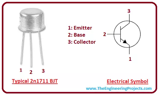
Hey Everyone! I hope you are doing great. We always come with some awesome topics related to engineering so you can excel and progress in your relevant field. Today, I am going to give you a brief details on the Introduction to 2n1711. It is an NPN (Negative-positive-Negative) bipolar junction transistor (BJT) which is mainly used for amplification and switching purpose. It encompasses low leakage current, high break down voltage, and low capacity which makes it useful over widely current range. I'll try to touch every aspect related to this transistor so you can get an idea what it does and what are its main applications? Let's get started.

Introduction to 2n1711

  • 2n1711 is an NPN bipolar junction transistor which is mainly used for switching and amplification applications.
  • It consists of three terminals called emitter base collector and comes in TO-39 case style.
  • It is a current controlled device where small current at the base side is used to control large current at the emitter and collector side.
  • 2n1711 is a bipolar device where conduction is carried out by movement of both charge carriers holes and electrons.
  • When we apply positive voltage at the base side, it gets biased and allows to control large current at the emitter and collector side.
  • Base is actually acts like a handle which actually controls the flow of electrons emitted by emitter.
  • These electron are then collected by collector. So base is actually controlling the conduction from emitter to collector terminals.
  • In this NPN transistor, emitter is heavily doped while base side is lightly doped.
  • Base side is positive with respect to emitter and P layer of this transistor lies between the two N-doped layers.
2n1711 Pinout
2n1711 mainly consists of three terminals which are described below. 1: Emitter 2: Base 3: Collector 
  • Small current at the base side is used to control the large current at the emitter and collector side.
  • This process of controlling large current with the help of small current is used for amplification purpose.
  • This transistor is mainly composed of silicon.
Circuit Diagram of 2n1711
Circuit symbol of 2n1711 is shown in the figure below.
  • This NPN transistor can be configured into three main configuration i.e common base configuration, common emitter configuration and common collector configuration.
  • Common emitter configuration is widely used for amplification purpose because it features the required voltage and power gain for amplification purpose.
  • This configuration allows the input to increase by 20dB which is nearly 100 times more than input signal.
  • It is important to note that collector voltage is higher than the base voltage.
  • Current at the emitter side is the combination of both base current and collector current.
  • Main difference between emitter and collector is their size and doping concentration. Collector is lightly doped while emitter is highly doped.
  • In this transistor, base current is always the smallest current while emitter current is always the largest current.
  • Forward current gain of the transistor is represented by beta ß. It is actually an amplification factor, the value at which current is being amplified. It is the ratio between collector current to the base current. As it is a ratio between two currents so it features no unit.
Absolute Maximum Ratings
Absolute maximum rating of 2n1711 is shown in the figure given below.
  • These are the stress ratings of 2n1711. If values are exceeded from given values, it can harm the device at large.
  • Collect base voltage is 75 V while collector emitter voltage is 50 V
  • Maximum power it can dissipate is 3 W.
Mechanical Outline of 2n1711
Mechanical outline of 2n1711 is shown in the figure below.
  • All dimensions are in mm.
  • You must take these dimension into consideration before you intend  to make a circuit so these dimensions can properly fit into the circuits.
Applications
  • 2n1711 is mainly used for amplification purpose.
  • In most of the circuits it is also used as a simple switch. When base is biased with the help of voltage, it allows the current to flow from emitter to collector. And in this state transistor remains in ON mode and acts as an ON switch. When there is no bias involved at the base side, the switch will be OFF.
This is all about the 2n1711 BJT. I hope you have enjoyed the article. I try my best to give you information divided in small step so you can digest the information without much effort. If still you feel any doubt or question, you can ask me in the comment section below. Your suggestions and feedback will be highly appreciated. Stay tuned for next article!

Introduction to 2sc4793

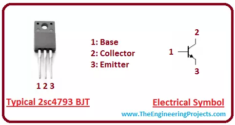
Hey Guys! I aspire you a very happy and promising life. My job is to give you daily dose of information so you can stand out of the party. Today, I am going to uncover the details on the Introduction to 2sc4793. It is an NPN (Negative-positive-negative) bipolar junction transistor (BJT) which is mainly used for amplification and switching purpose. I'll give you a brief details about this transistor and try to cover as many aspects as possible related to this transistor. Let's hop on the board and explore what kind of transistor is this and what are its main applications? Let's get started.

Introduction to 2sc4793

  • 2sc4793 is an NPN bipolar junction transistor where P-doped layer is sandwiched between the two N-doped layer.
  • It is mainly three terminal device which comes in TO-220F package and exhibits high transition frequency.
  • Three terminals are called emitter base and collector.
  • P layer of this transistor is behaved like a base while other two N layers represent collector and emitter receptively.
  • As it is an NPN transistor, so base is positive with respect to emitter.
  • It is a current controlled device where small current at the base side is used to control the large amount of current at the emitter and collector side.
  • Unlike FETs(Field effect transistors), it is a bipolar device, where conduction is carried by the movement of both charge carriers i.e. electrons and holes.
  • Sometimes you can see these transistor separated but most of the time they are incorporated in tiny integrated circuit.
  • This transistor is widely used in many electronic application but mostly it is used for amplification and switching purpose.
2sc4793 Pinout
2sc4793 bipolar junction transistor mainly consists of three terminals. 1: Base 2: Collector 3: Emitter
  • The small current at the base side is used to control the large current at the collector and emitter side.
  • The ability of base current to control emitter and collector current is used for amplification purpose.
  • This silicon transistor is mainly remained in ON state when current flows from emitter to collector.
Circuit Diagram of 2sc4793
Following figure shows the circuit symbol of 2sc4793.  
  • As it is an NPN transistor, so base is positive as compared to emitter.
  • In most NPN transistors, emitter side is heavily doped because its job is to emit number of electrons while base side is lightly doped because its job is to control the number of electrons emitted from the emitter side.
  • These injected electrons are then collected by the collector. Hence, base controls the overall conductivity of the path between emitter and collector.
  • Forward current gain of this transistor can be represented as Beta ß.
  • It is a ratio between collector current and base current and it exhibits no units.
  • Sometimes it is referred as a amplification factor because small change in base current causes a large change in collector current.
  • Beta value ranges between 20 to 1000. Standard value in most of the cases is 200.
  • The current gain of the transistor is represented by alpha a and it is a ratio between collector current and emitter current.
  • Alpha value of transistor ranges between 0.95 to 0.99, however in most of the cases alpha value is considered as one.
  • When voltage is applied at the base side, it gets biased and allows the current to flow from emitter to collector.
  • When there in no voltage at the base side, transistor will be OFF, in case of positive voltage at the base, transistor is considered as ON.
Absolute Maximum Rating of 2sc4793
Absolute maximum rating of 2sc4793 is shown in the figure below.
  • Both, collector-base and collector-emitter voltage are 230 V. Collector current is 1 A and base current is 0.1 A. Maximum power it can dissipate is about 20 W.
  • These are the standard stress rating. Values above these standard operating conditions can damage the device and can effect device reliability.
Applications
  • 2sc4793 is widely used in many electronic circuits as a voltage and power amplifiers.
  • It is also used as switch in most circuits, because it exhibits high transition frequency.
That's all for today. Hope you have enjoyed the article and got a clear idea about this BJT. However, if still you feel any doubt or have any query, you can ask me in the comment section below. I'll try my best to resolve your query according to best of my expertise. Your feedback and suggestion will be highly appreciated. It will allow us to give you quality work that resonates with your needs and expectations. Stay tuned!

Introduction to Lm324n

Hey Guys! Hope you are doing great and having fun. Today, I am going to unlock the details on the Introduction to Lm324n. It is a seven pin operational amplifier that comes in discrete and compact single package. It is a high gain voltage amplifier, where output voltage signal is much higher than the input voltage signal. I'll try my best to cover as many aspects as possible related to this operational amplifier so you don't need to go any where and you find all information at one place. Let's get started. [otw_is sidebar=otw-sidebar-7]

Introduction to Lm324n

  • Lm324n is a high gain voltage amplifier that comes with differential input and single ended output.
  • It is designed in such a way, that the voltage difference between input terminals creates an output signal of much larger magnitude.
 
  • It consists of four independent op-amp that are incorporated in a single 14 pin DIP package.
  • Operational amplifiers are the initial devices that were used in analog computer to perform many mathematical operations in many nonlinear and linear circuits.
  • Lm324n mostly operates on a single power supply and with wide range of voltages.
  • We can also operate this device on a split power supply however, supply current drain doesn't depend on the strength of supply voltage.
  • The characteristic of this circuit, its band width, impedance, and input don't effect manufacturing variations and temperature coefficient because this op-amp exhibits negative feedback.
  • Op-amp are widely used in many electronic applications as oscillator, rectifier and comparators  and are most common scientific devices these days.
  • Output voltage of this amplifier goes to ground and it also allows direct sensing ground. Lm324n is compatible with all forms of logic circuits.
  • Power drain incorporated in this amplifier is suitable for battery operation.
  • In the linear mode of operation, voltage ranges between ground and out put voltage.
  • The unity gain cross frequency and input bias current of this amplifier is temperature compensated.
  • Normally operational amplifiers amplifies the difference between the input voltage which is normally called the differential input voltage.
  • The differential inputs of this amplifier consists of inverting input voltage with V_ and non-inverting input voltage with V+. The output of the this op-amp is given by

V(out)= AoL(V+ _ V_)

  • Here AoL represents the open loop gain of the amplifier. As it is an open loop gain so it doesn't contain feedback from output to the input.
  • The magnitude of AoL is very high sometimes goes to 100,000, so small difference between non-inverting and inverting voltages magnifies the output voltage to nearly supply voltage.
  • A state in which output voltage is equal or greater than input supply voltage is called saturation state of the amplifier.
  • It is important to note magnitude of open loop gain of the amplifier can not be controlled by the manufacturing process, so open loop amplifier can not be used as a standalone differential amplifier.
  • Op-amp is behaved like a comparator in the absence of negative feedback.
  • If positive voltage is applied at the non-inverting terminal and inverting terminal is set to ground with the help of resister, then the output will turn out to be maximum positive and if negative voltage is applied on the non-inverting terminal the output voltage will be maximum negative.
Lm324n Pinout
Pinout of Lm324n is shown in the figure below.
  • It mainly consists of 14 pins. Function of each pin is shown in the figure below.
  • Lm324n operates on a single power supply and contains true differential inputs that operate in linear mode.
  • It can operate over a multiple range of power supply voltage which have little impact on performance characteristics.
  • At 25 ºC, Lm324n can operate over a minimum voltage supply of 2.3V.
Absolute Maximum Rating Lm324n
Absolute maximum rating of Lm324n is shown in the figure below.  
  • It is important to note that input voltage shown in the figure above will only exist when voltage at any input terminals is driven negative.
  • This happens because collector base junction of PNP transistors turns to forward biased mode, which ultimately behaves as input diode clamps.
  • This transistor action allows the output voltage oscillates between positive voltage supply and ground.
  • It will only happen between the time duration when input is driven negative.
  • Short circuits from output to the positive supply voltage can create excessive heating which ultimately damages the device.
Functional Block Diagram
Following figure shows the functinal block diagram of Lm324n.
  • There is no need of diodes for differential voltage protection because large differential input voltages don't exhibit large current.
  • The differential input voltage can exceed from input positive voltage without harming the device.
  • However, protection must be needed in order to avoid input voltage from going too negative below than _ 0.3 V. A simple diode with resistor can be used as a protection on the input of voltage terminals.
  • In order to minimum the power drain, these amplifies have Class A output stage for small signals which evidently convert to Class B out put stage for large signals.
  • This action causes the amplifiers to sink and source the large current. Both, NPN and PNP resistors can be used to increase the power intensity of the basic amplifiers.
  • In most of the AC application, output of the load is capacitively connected with amplifier, A resistor must be connected to the amplifier out put and ground in order to avoid crossover distortion and to enhance class A bias current.
  • No cross over distortion is observed when out put load is directly connected with the amplifier.
Applications
  • Lm324n is widely used in transducer amplifiers.
  • DC gain blocks and conventional amplifiers circuits are mainly consists of Lm324n.
  • It can be used as a rectifier, oscillator and comparator.
That's all for today. I hope you have got a clear idea about this amplifier. However, if you have any question or query regarding this amplifier, you can ping me a comment in the section below. I'll try my best to help you in this regard. Stay tuned!
Syed Zain Nasir

I am Syed Zain Nasir, the founder of <a href=https://www.TheEngineeringProjects.com/>The Engineering Projects</a> (TEP). I am a programmer since 2009 before that I just search things, make small projects and now I am sharing my knowledge through this platform.I also work as a freelancer and did many projects related to programming and electrical circuitry. <a href=https://plus.google.com/+SyedZainNasir/>My Google Profile+</a>

Share
Published by
Syed Zain Nasir