Introduction to ATmega8

Hi Friends! Hope you are doing well. I am back to give you a daily dose of useful information so you can excel and improve as per your technical needs and requirements. Today, I'll uncover the details on the Introduction to ATmega8. It is an 8-bit AVR microcontroller that is based on RISC CMOS technology and comes with a 28-pin interface for the PDIP package. The Program memory is 8K Flash while RAM and EEPROM are 1K and 512 bytes respectively.

Microchip has been the main source for producing PIC and AVR microcontrollers that are mainly used in embedded and industrial automation systems. These modules can perform a number of functions on a tiny chip, preventing you from spending too much and purchasing external components for laying out automation in the relevant project.

In this post, I’ll cover each and everything related to this tiny chip including main features, pinout, pin description, functions, the compiler used and everything you need to know. Let’s get down to the details of this onboard module:

Introduction to ATmega8

  • ATmega8 is a 28-pin, 8-bit AVR microcontroller, based on RISC architecture, designed by Microchip and is mainly used in the embedded systems and industrial automation projects.
  • It comes in three packages known as PDIP, MLF, and TQFP, where the first one contains 28 pins and the other two come with 32-pin on each module.
  • The Program memory(Flash Memory) is 8KB used to store the programming code and permanent settings.
  • Atmega8 comes with a RAM memory of 1KB, it's a volatile memory and refreshes on restart.
  • It also has an EEPROM memory of 512 bytes, which is a semi-volatile memory.
  • Other features includes are a power-up timer, a watchdog timer, Brown out Detection, In-Circuit Serial Programming and five sleep modes.
  • The instruction set is the main criteria that set this module apart from the PIC microcontroller where the former executes most instructions in one clock cycle and comes with 32 general-purpose registers while later requires a number of clock cycles per instruction and comes with W register.
  • The 10-bit ADC module is added to the device that plays a vital role for sensor interfacing and contains a total of 6 channels for the PDIP package and 8 channels for the remaining two packages.
  • Communication protocols like SPI, I2C, and USART are added to the device that is widely used for establishing communication with external devices.

ATmega8 Key Features

  • Before you start working on the relevant project, it is advised to check the features of the module, in order to get an idea if these features are suitable for the project you aim to work on.
  • The following table shows the main features of ATmega8.
Atmega8 Key Features
No. of Pins 28
CPU 8-Bit AVR
Operating Voltage 2.7 to 5.5 V
Program Memory 8K
Program Memory Type Flash
RAM 1K Bytes
EEPROM 512 Bytes
ADC Number of ADC Channels 10-Bit 6 in PDIP, 8 in TQFP and QFN
Comparator 1
PWM Channels 3
Oscillator up to 16 MHz
Timer (3) 16-Bit Timer (1) 8-Bit Timer (2)
Packages (3) PDIP (28-Pins) TQFP (32-Pins) QFN (32)
Power Up Timer Yes
I/O Pins 23
Manufacturer Microchip
SPI Yes
I2C Yes
Watchdog Timer Yes
Brownout Detection (BOD) Yes
USART Yes
Sleep Modes 5
Minimum Operating Temperature -55 C
Maximum Operating Temperature 125 C

ATmega8 Pinout and Description

  • You have got a brief introduction to the module. In this section, we will cover the pinout and description of each pin.

Pinout

  • The following figure shows the pinout of ATmega8.
  • ATmega8 comes in three packages known as PDIP, MLF, and TQFP where the first is used for prototype projects, while the other two are used for industrial and electronic devices.
  • The following table shows the complete description of each pinout, which will help you anticipate the major function associated with each pin.
Atmega8 pinout & Description
1 PC6 RESET PCINT14 I/O Pin RESET will be generated by keeping this pin LOW for longer than the minimum pulse length Interrupt
2 PD0 RXD PCINT16 I/O Pin Serial Receive Pin (USART) Interrupt
3 PD1 TXD PCINT17 I/O Pin Serial Transmit Pin (USART)Interrupt
4 PD2 INT0 PCINT18 I/O Pin External Interrupt Interrupt
5 PD3 INT1 OC2B PCINT19 I/O Pin External Interrupt Dedicated Pin for Timer (PWM Channel) Interrupt
6 PD4 T0 XCK PCINT20 I/O Pin T0 ( Timer0 External Counter Input) XCK ( USART External Clock I/O) Interrupt
7 VCC Voltage Supply
8 GND Ground Pin
9 PB6 OSC1 XTAL1 PCINT6 I/O Pin Oscillator Input Pin Interrupt
10 PB7 OSC2 XTAL2 PCINT7 I/O Pin Oscillator Output Pin Interrupt
11 PD5 T1 OC0B PCINT21 I/O Pin PinT1 ( Timer0 External Counter Input) Dedicated Pin for Timer (PWM Channel) Interrupt
12 PD6 AIN0 OC0A PCINT22 I/O PinAnalog Comparator Positive Dedicated Pin for Timer (PWM Channel) Interrupt
13 PD7 AIN1 PCINT23 I/O Pin Analog Comparator Negative Interrupt
14 PB0 ICP1 CLKO PCINT0 I/O Pin In Circuit Serial Programming Clock Interrupt
15 PB1 OC1A PCINT1 I/O Pin Dedicated Pin for Timer (PWM Channel) Interrupt
16 PB2 SS OC1B PCINT2 I/O Pin SPI Slave Select Input. When the controller acts as a slave, this pin is LOW Dedicated Pin for Timer (PWM Channel) Interrupt
17 PB3 MOSI OC2A PCINT3 I/O Pin MOSI (Master Output Slave Input) for SPI Communication. The data is received by this pin when the controller acts as a slave Dedicated Pin for Timer Interrupt
18 PB4 MISO PCINT4 I/O Pin MISO (Master Input Slave Output) for SPI communication. When the controller acts as a slave, the data is sent by a controller to master through this pin Interrupt
19 PB5 SCK PCINT5 I/O Pin SCK (SPI Bus Serial Clock). This clock is shared between the controller and other devices for data transfer Interrupt
20 AVCC Voltage Supply Pin for ADC
21 AREF Voltage Reference
22 GND Ground Pin
23 PC0 ADC0 PCINT8 I/O Pin Analog Channel 0 Interrupt
24 PC1 ADC1 PCINT9 I/O Pin Analog Channel 1 Interrupt
25 PC2 ADC2 PCINT10 I/O Pin Analog Channel 2 Interrupt
26 PC3 ADC3 PCINT11 I/O Pin Analog Channel 3 Interrupt
27 PC4 ADC4 SDA PCINT12 I/O Pin Analog Channel 4 Serial Data (I2C) Interrupt
28 PC5 ADC5 SCL PCINT13 I/O Pin Analog Channel 5 Serial Clock (I2C) Interrupt

ATmega8 Main Functions

  • ATmega8 comes with the ability to execute and perform a number of functions.
  • Following are the major functions related to this tiny module.

Timer

Atmega8 incorporates three timers where two are 8-bit and one is a 16-bit timer.  These timers can be used both ways i.e. timer as well as a counter where the former is used to create the delay in any running function, controls the internal functions of the controller and increments the instruction cycle, while later is used to count the number of intervals by incrementing the rising and falling edge of the pin and is mainly used for external functions. Apart from these timers, two other timers are included in the device named as

  • Oscillator Start-up Timers
  • Power Up Timer

An oscillator start-up timer is used to make the crystal oscillator stable by resetting the controller. And power-up timer generates a minor delay once you power on the device, helping in stabilizing the power in order to generate power signals with continuous intervals.

Number of Sleep Modes

Five Sleep Modes are incorporated into the device that helps in saving power. These modes include:

  • Power-save
  • Power-down
  • Idle
  • ADC Noise Reduction
  • Standby

Brown Out Detect (BOD)

The BOD, also known as BOR (Brown Out Reset), is used to resetting the module once the Vcc (voltage supply) goes below a brownout threshold voltage. It is important to note that, the Power Up Timer must be enabled for creating a delay and helping in bringing back the device from a BOD function. In this mode, multiple voltage ranges are created to protect the module once the power drops at the voltage supply line.

SPI Communication

ATmega8 comes with a serial peripheral interface (SPI) - A communication module that helps in establishing communication between the microcontroller and other peripheral devices such as shift registers, SD cards, and sensors. It incorporates a separate clock and data lines with the addition of a select line for selecting the relevant device for communication.

Two pins used for SPI communication are as follow:

  • MOSI (Master Output Slave Input)
  • MISO (Master Input Slave Output)

The MOSI pin receives the data when the controller acts as a slave. And MISO plays a vital role in sending data by the controller while later is put in the slave mode.

Watchdog Timer

ATmega8 incorporates a built-in watchdog timer that resets the controller if the running program hangs up during compilation or gets stuck in the infinite loop. The watchdog timer is nothing but a countdown timer.

Interrupt

The interrupt hints at a call of emergency that puts the main function on hold until the required instruction is executed. The controller goes to the main program once the interrupt is called and executed.

I2C Communication

  • I2C protocol is used to connect low-speed devices like ADC and DAC converters, and microcontrollers.
  • It is a two-wire communication that comes with:
    • Serial Clock (SCL)
    • Serial Data (SDA)

The former is a clock signal that synchronizes the data transfer between the devices and is produced by the master device, while the latter is used to carry the required data.

ATmega8 Memory Interface

The memory space in the controller is the manifestation of the linear and regular memory map. This AVR module comes with a Harvard Architecture that houses separate memories for both data and program.

  • Single pipelining is used for the executions of the instructions in the Program Memory - A programmable Flash Memory - where the next instruction is called and executed followed by the next instruction that helps in executing the instructions in every clock cycle.

The Fast Access File Register comes with 32 x 8 - Bit general purpose working registers that can be accessed with the single clock cycle that assists in performing the ALU (Arithmetic Logic Unit) operation where the result is stored in the Register File.

The I/O Memory can be accessed in multiple ways by direct manner or using data Space locations covering Register File, 0x20 – 0x5F.

Program Memory (ROM)

  • Program memory comes with a memory space around 8K and can perform the instructions in every clock cycle.
  • It stores information permanently and doesn't depend on the source of power supply and is widely known as ROM or Non-Volatile Memory.
  • The program memory address can access 16 or 32-bit instruction.
  • Program Flash is divided into two parts including the Application Program section and the Boot Program section.
  • The latter comes with Applications Flash Memory used for SPM instruction writing.

Data Memory (RAM)

The data memory comes with memory space around 1K (1024 bytes). It can be accessed through the five different addressing modes in the AVR architecture named Direct, Indirect, Indirect with Displacement, Indirect with Pre-decrement, and Indirect with Post-increment.

  • Three address registers X, Y, and Z are capable to increment and decrement with regular intervals in the presence of indirect addressing modes.

The flexible interrupt module houses control registers that further contain global interrupt enable bit sitting in the Status Register. All these interrupts contain Interrupt Vector Table with Interrupt Vector where the former depends on the Interrupt Vector Position and are inversely proportional to each other.

  • The ALU module, which is divided into three major functions known as direct, arithmetic and bit functions, has a direct connection with 32 general-purpose registers within a single clock cycle.

ATmega8 Compilers

If you are new to a microcontroller, you may be a little skeptical about the compiler you can use for writing and compiling the code into your AVR controller. I've combined some of the basic compilers where some are better than others in terms of efficiency. Although the free versions may lack some features, they are recommended to start with as a newbie to get hands-on experience with the AVR controller.

  • The IAR compiler proves to be the best compiler for AVR. Although it is expensive and incorporates a highly professional interface.
  • The GCC Port is a good option for AVR that works with both Linux and Windows. The interface is a little bit complex.
  • ImageCraft is another right option to start with, but it lacks some GUI features like editor and project management that may create trouble during the execution of code.
  • CodeVision comes with CodeWizard and is highly economical.

6. ATmega8 Interfacing with Arduino

ATmega8 can be interfaced with Arduino for the development of the embedded project. The following figure shows the interfacing of ATmega8 with Arduino.
  • If you are new to the Arduino Board, you must try these Arduino Projects for Beginners, they will help understand the major functions of the Arduino Board.

ATmega8 Internal Block Diagram

  • A Block diagram will help you get a hold of how major functions and components are connected and perform inside the device.
  • The following figure shows the block diagram of ATmega8:
  • ATmega8 is a low-power CMOS AVR microcontroller that is mainly based on RISC architecture. By executing powerful instructions in a single clock cycle, the ATmega8 is capable to perform and execute powerful instructions using 1MIPS per MHz in a single clock cycle that drastically helps in optimizing the power consumption.

8. ATmega8 Projects and Applications

  • Used in embedded and robotics system
  • It is widely used in students projects
  • Home Security System
  • For the designing of quadcopters
  • Industrial Automation
That's all for today. I hope you have found this article information. If you are unsure or have any questions, you can approach me in the comment section below. I'd love to help you the best way I can. Feel free to feed us with your valuable suggestions - they help us provide you quality work. Thanks for reading the article.

Introduction to ATmega168

Hi Friends! Hope you are doing well. We always strive to give you valuable information as per your needs and requirements so you keep coming back for what we have to offer. Today, I'll uncover the details on the Introduction to ATmega168. It is an 8-bit AVR microcontroller that comes with 32-pin interface and is mainly based on RISC CMOS technology. The Program memory is 16K, based on Flash, and incorporates read-write capabilities. The module comes with a wide temperature range from -40 to 85 ºC while operating voltage ranges from 1.8 to 5.5 V. If you are working on project that is related to automation and embedded systems, you can not write off the importance of this module that comes with an ability of performing a number of functions at once on a single chip. In this post, I'll cover each and everything related to this module including main features, pinout, pin description, functions, the compiler used and real-time applications. Let's jump right it, and get down to the nitty-gritty of this little toy.

Introduction to ATmega168

  • ATmega168 is an 8-bit AVR microcontroller that comes in three packages named as PDIP, MLF, and TQFP, where the first two contain 28 pins on each module while other comes with 32-pin interface.
  • The Program memory is 16K that is based on Flash while other two memories RAM and EEPROM contain 1K and 512 Bytes respectively with data retention capability of around 20 years.
  • The 10-bit ADC module is added in the device that plays a vital role for sensor interfacing and contains total 8 channels that are enough to provide analog to digital conversion to a number of pins.
  • Only a few controllers incorporate all three communication protocols i.e. SPI, I2C and USART and ATmega168 is one of them. These protocols are widely used for setting up a communication with external devices.
  • Apart from providing decent pace for executing a number of instructions, other features this module includes a watchdog timer, power up timer, oscillator start-up timer, Brown out Detection and In-Circuit Serial Programming.
  • What Makes this AVR module Different from PIC Microcontrollers is the instruction set. PIC microcontrollers require a number of clock cycles per instruction while AVR executes most instructions in one clock cycle. Also, PIC contains a 'W' register, while AVR comes with 32 general purpose registers where three pairs can be employed as pointers.

1. ATmega168 Features

Features of any device are very important to get a hold of major functions and characteristics associated with it. Following table shows the main features of this module.
ATmega168 Features
No. of Pins 28
CPU RISC 8-Bit CMOS
Operating Voltage 1.8 to 5.5 V
Program Memory 16K
Program Memory Type Flash
RAM 1K
EEPROM 512 Bytes
ADC Number of ADC Channels 10-Bit 8
Comparator 1
In-circuit serial programming Yes
Oscillator up to 20 MHz
Timer (3) 16-Bit Timer (1) 8-Bit Timer (2)
Capture/Compare/PWM 1/1/6
Power Up Timer Yes
I/O Pins 23
USART Yes
SPI 2
I2C Yes
Watchdog Timer Yes
Brown out Detection (BOD) Yes
Power on Reset Yes
Data Retention 20 Years
Minimum Operating Temperature -40 ºC
Maximum Operating Temperature 85 ºC

2. ATmega168 Pinout and Description

In this section, we will cover the pinout and pin description of each pin of the controller so you can anticipate the main functions associated with the pins. The following figure shows the pinout of ATmega168.
  • ATmega168 comes in three packages named as PDIP, MLF, and TQFP where first is used for the development of individual projects while the other two are added to the industrial and electronic devices.
Pin Description
Following table shows the pin description of each pin that will help you foresee the major functions associated with each pin of the controller.
Pin# Pin Name Pin Description
1 PC6 RESET PCINT14 Digital I/O Pin RESET will be generated by keeping this pin LOW for longer than the minimum pulse length Interrupt
2 PD0 RXD PCINT16 Digital I/O Pin Serial Receive Pin (USART) Interrupt
3 PD1 TXD PCINT17 Digital I/O Pin Serial Transmit Pin (USART) Interrupt
4 PD2 INT0 PCINT18 Digital I/O Pin External Interrupt Interrupt
5 PD3 INT1 OC2B PCINT19 Digital I/O Pin External Interrupt Dedicated Pin for Timer (PWM Channel) Interrupt
6 PD4 T0 XCK PCINT20 Digital I/O Pin T0 ( Timer0 External Counter Input) XCK ( USART External Clock I/O) Interrupt
7 VCC Voltage Supply
8 GND Ground Pin
9 PB6 OSC1 XTAL1 PCINT6 Digital I/O Pin Oscillator Input Pin Interrupt
10 PB7 OSC2 XTAL2 PCINT7 Digital I/O Pin Oscillator Output Pin Interrupt  
11 PD5 T1 OC0B PCINT21 Digital I/O Pin T1 ( Timer0 External Counter Input) Dedicated Pin for Timer (PWM Channel) Interrupt  
12 PD6 AIN0 OC0A PCINT22 Digital I/O Pin Analog Comparator Positive Dedicated Pin for Timer (PWM Channel) Interrupt    
13 PD7 AIN1 PCINT23 Digital I/O Pin Analog Comparator Negative Interrupt
14 PB0 ICP1 CLKO PCINT0 Digital I/O Pin In Circuit Serial Programming Clock Interrupt
15 PB1 OC1A PCINT1 Digital I/O Pin Dedicated Pin for Timer (PWM Channel) Interrupt
16 PB2 SS OC1B PCINT2 Digital I/O Pin SPI Slave Select Input. When the controller acts as a slave, this pin is LOW Dedicated Pin for Timer (PWM Channel) Interrupt
17 PB3 MOSI OC2A PCINT3 Digital I/O Pin MOSI (Master Output Slave Input) for SPI Communication. The data is received by this pin when the controller acts as a slave Dedicated Pin for Timer Interrupt
18 PB4 MISO PCINT4 Digital I/O Pin MISO (Master Input Slave Output) for SPI communication. When the controller acts as a slave, the data is sent by a controller to master through this pin Interrupt
19 PB5 SCK PCINT5 Digital I/O Pin SCK (SPI Bus Serial Clock). This clock is shared between the controller and other devices for data transfer Interrupt
20 AVCC Voltage Supply Pin for ADC
21 AREF Voltage Reference
22 GND Ground Pin
23 PC0 ADC0 PCINT8 Digital I/O Pin Analog Channel 0 Interrupt
24 PC1 ADC1 PCINT9 Digital I/O Pin Analog Channel 1 Interrupt
25 PC2 ADC2 PCINT10 Digital I/O Pin Analog Channel 2 Interrupt
26 PC3 ADC3 PCINT11 Digital I/O Pin Analog Channel 3 Interrupt
27 PC4 ADC4 SDA PCINT12 Digital I/O Pin Analog Channel 4 Serial Data (I2C) Interrupt
28 PC5 ADC5 SCL PCINT13 Digital I/O Pin Analog Channel 5 Serial Clock (I2C) Interrupt

3. ATmega168 Main Functions

ATmega168 comes with an ability to execute and perform a number of functions. Following are the major functions related to this tiny module.
Timer
Atmega168 comes with three timers where two are 8-bit and one a 16-bit timer.  These timers can be used as a timer as well as a counter. The timer mode is used to create the dealy in any running function that increments the instruction cycle and mainly controls the internal functions of the controller. While the counter mode counts the number of intervals in any function and is mainly used for external functions where it can increment the rising and falling edge of the pin.
  • Oscillator Start-up Timers
  • Power Up Timer
Oscillator start-up timer resets the controller until the crystal oscillator becomes stable. Similarly, power-up timer is added that generates a minor delay once you power on the device, that provides an appropriate time to stabilize the power where it can generate power signals in a continuous manner.
Brown Out Detect (BOD)
The BOD, also known as BOR (Brown Out Reset), is a very valuable function that resets the module once the Vcc (voltage supply) goes below a brownout threshold voltage. In this mode, multiple voltage ranges are used and generated to protect the module once the power drops at the voltage supply line, setting you free from manually resetting the device. The Power Up Timer must be enabled, that creates the delay in bringing back the device from a BOD function.
Number of Sleep Modes
Six Sleep Modes are added to the device that help in saving power. These modes include:
  • Idle
  • ADC Noise Reduction
  • Power-save
  • Power-down
  • Standby
  • Extended Standby
SPI Communication
ATmega168 incorporates a serial peripheral interface (SPI) that nails down a communication between the microcontroller and other peripheral devices such as SD cards, shift registers, and sensors. It comes with separate clock and data lines with the addition of a select line to select the given device for communication. Two pins called used for SPI communication are as follow MOSI (Master Output Slave Input) MISO (Master Input Slave Output) The data is received by MOSI pin when the controller acts as a slave. And MISO is responsible for sending data by the controller when later acts as a slave.
Interrupt
The interrupt is used for a call of emergency which puts the main function on hold and executes the required instructions essential at that time. Once the interrupt is called and executed the running instruction brings the controller back to the main program.
I2C Communication
I2C protocol is a two-wire protocol used to connect low-speed devices like ADC and DAC converters, and microcontrollers. It comes with two wires called Serial Clock (SCL) Serial Data (SDA)  The former behaves like a clock signal that is produced by the master device and synchronizes the data transfer between the devices. And the later is used to carry the desired data.
Watchdog Timer
ATmega168 comes with a built-in watchdog timer that brings the controller back in reset position if the program hangs up during compilation or gets stuck in the infinite loop. The watchdog timer acts like a countdown timer in the running function.

4. ATmega168 Memory Interface

This AVR controller encompasses the Harvard Architecture that provides separate memory locations for both Data and Program memory. The memory is based on Atmel’s high-density technology where Program Memory, also known as Flash memory, can be reprogrammed through SPI serial interface using two ways i.e. Non-volatile memory programmer or On-chip boot code. The CPU is very useful to access memories and perform calculations on the basis of the number of instructions fed into the controller.
Program Memory (ROM)
Program memory performs the instructions in every clock cycle at regular intervals. It is also known as ROM or non-volatile memory that stores the information permanently and works perfectly in the absence of power supply.
  • The controller program memory executes the required instruction followed by the next instruction. Every program memory address is able to access a 16- or 32-bit instruction.
Program memory comes with a memory space around 16K - lot more than some other controllers available in the AVR community.
  • Program Flash is mainly categorized into two sections i.e. Application Program section and the Boot Program section. Lock bits are reserved for read/write protection. The Boot Program Section houses Application Flash Memory that is responsible for SPM instruction writing.
Data Memory (RAM)
The data memory contains 1K (1024 bytes) memory space. It categorizes the memory locations three ways where first 32 locations access the file register, next 64 locations are allocated for standard I/O memory and remaining are employed for internal data SRAM. The data memory is categorized into five addressing modes known as
  • Direct,
  • Indirect
  • Indirect with Displacement
  • Indirect with Pre-decrement
  • Indirect with Post-increment
The memory space in the controller shows the linear and regular memory map. The address registers X, Y, and Z can increment and decrement with regular intervals when indirect addressing modes are coupled with both pre-decrement and post-increment. It is important to note that, the I/O Memory can be accessed in two ways i.e. using data Space locations covering Register File, 0x20 - 0x5F or in a direct manner.

5. ATmega168 Compilers

Compilers are used for writing and compiling the code in the AVR microcontroller. Following are some compilers you can use for this AVR module.
  • The IAR is the best compiler for AVR. It is expensive and incorporates highly professional interface. If you are a beginner, it is advised to use this compiler as per your technical needs and requirements.
  • CodeVision is cheap and easy to use that incorporates CodeWizard.
  • The GCC Port is another compiler for AVR. It is available FREE for both Linux and Windows operating systems. It comes with little bit complex interface that may put you in trouble right off the bat.
  • ImageCraft is a valuable option but it lacks some GUI features where editor and project management are quite formidable and can create trouble for the code execution.

6. ATmega168 Interfacing with Arduino

ATmega168 can be interfaced with Arduino to drive automation in the relevant project. Both modules work perfectly in embedded systems where they can perform a number of useful functions. The following figure shows the pinout how Arduino pins are connected with ATmega168.
  • If you aim to work on this Arduino board then you must try these Arduino Projects for Beginners, they will help to get familiar with the Arduino Board.

7. ATmega168 Block Diagram

If you intend to closely look into the device and how major functions and components are connected and performed inside the device, a block diagram will help you out. The following figure shows the block diagram of ATmega168.
  • AVCC is a voltage supply for analog to digital converter that is necessary to power up the ADC module. Power on reset and brown out detect house in the same package that is also connected with the watchdog timer.

8. ATmega168 Projects and Applications

  • It is widely used in students projects
  • Used in embedded and robotics system
  • Industrial Automation
  • Home Security System
  • For the designing of quadcopters
That's all for today. I hope you have found this article useful. If you are feeling skeptical or have any question, you can approach me in the comment section below. I'd love to help you in any way I can according to the best of my expertise. Feel free to keep us updated with your valuable suggestion, they help us provide you quality work as per your needs and demands. Thanks for reading the article.

Introduction to ATtiny85

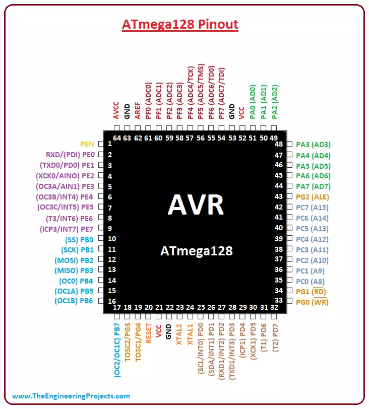
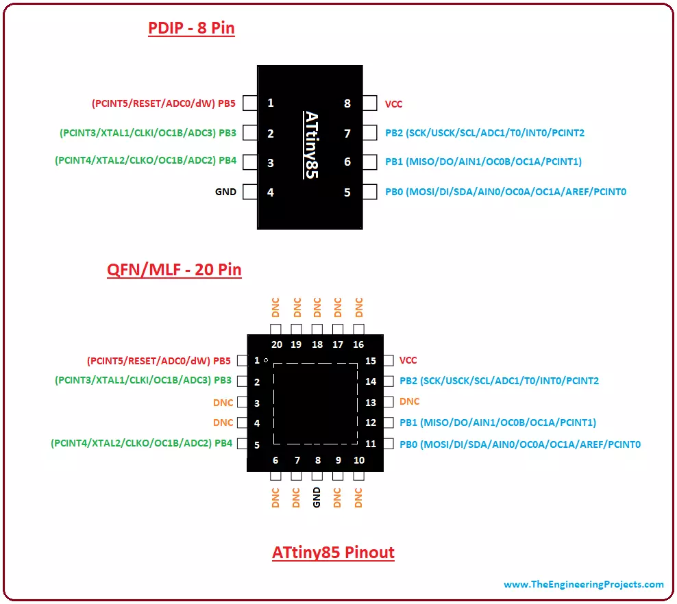
Hey Guys! Hope you are doing well. I am back to give you a daily dose of valuable information. Today, I'll discuss the details on the Introduction to ATtiny85. It is an 8-bit AVR microcontroller, introduced by Microchip, and is based on RISC CPU. It comes with 8-pin interface (PDIP) and falls under the category of low power controllers. Programmable watchdog timer and 10-bit ADC converter are added in the device that makes it suitable for sensor interfacing and resetting the device in case it gets stuck in an infinite loop. Microchip never fails to satisfy the requirements of any individual by providing flawless microcontroller modules that are directly or remotely connected with automation and embedded systems. With the invention of these tiny onboard modules, development of electronic projects has become easy and hassle-free more than ever before. In this tutorial, I'll cover each and everything related to ATtiny85, its pinout, pin description, main features, block diagram, and applications. Let get down to the nitty-gritty of this module and nail down everything you need to know.

Introduction to ATtiny85

  • ATtiny85 is an 8-bit AVR microcontroller that comes with 8-pin interface and mainly used in automation and Arduino projects.
  • The CPU is based on RISC architecture and is mainly called low power controller that stands fit for the real-time applications that can operate on minimum power.
  • The program memory is 8KB while both EEPROM and RAM contain a memory space of around 512 bytes. These memory spaces are very useful for storing the number of instruction in the form of code.
  • This module comes with only one port called Port B that is a bi-directional port and contains 6 I/O pins with internal pull-up resistors. The output buffers on PORTB are designed with symmetrical drive characteristics that come with both high sink and source capability. It is important to note that, Port B pins are externally pulled low and tri-stated that will source current if the pull-up resistors are activated.
  • External and internal interrupts are available on the board, while 32 general purpose registers are included in the device that are mainly called data holding spaces.
  • Two 8-bit timers are added in the device where one timer comes with compare modes and can be used both ways i.e. timer as well as a counter while other is high-speed timer/counter.
  • This module comes with software select power saving modes that are very helpful for the applications that operate with minimum power.
  • Like other controllers introduced by the Microchip, this module comes with 10-bit ADC converter that houses 4 analog channels that help in sensor interfacing and converting analog signals to digital ones.
  • This tiny chip is available in four packages called PDIP, SOIC, TSSOP, and QFN where first three come with 8-pin interface while the last one contains 20 pins.
  • Digital communications like I2C and SPI can be easily employed using this module that helps in developing a communication with external devices.

1. ATtiny85 Features

You have got a brief overview of this module. Now we cover the main features that will help you anticipate the major characteristic associated with the module. The following figure shows the complete features of ATtiny85.
ATtiny85 Features
No. of Pins 8
CPU RISC 8-Bit AVR
Operating Voltage 1.8 to 5.5 V
Program Memory 8K
Program Memory Type Flash
RAM 512 Bytes
EEPROM 512 Bytes
ADC Number of ADC Channels 10-Bit 4
Comparator 1
Packages PDIP (8-Pin) SOIC (8-Pin) TSSOP (8-Pin) QFN/MLF (20-Pin)
Oscillator up to 20 MHz
Timer (2) 8-Bit Timers
Enhanced Power on Reset Yes
Power Up Timer Yes
I/O Pins 6
Manufacturer Microchip
SPI Yes
I2C Yes
Watchdog Timer Yes
Brown out detect (BOD) Yes
Reset Yes
USI (Universal Serial Interface) Yes
Minimum Operating Temperature -40 C
Maximum Operating Temperature 125 C
  • You must check these features before making a final decision to install and use this module for your relevant project.

2. ATtin85 Pinout and Description

Until now, you have got a hold of basic information and complete features of ATtiny85. In this section, we will discuss the pinout and pin description of the module.
Pinout
Following figure shows the pinout of ATtiny85.
  • The bottom pad available on the board must be soldered to the ground.
  • The DNC marked on the pinout stands for don't connect.
Pin Description
Following table shows the pin description that will help you understand the major functions associated with each pin.
Pin# Pin Name Pin Description
1 PB5 PCINT5 RESET ADC0 dW I/O Bidirectional pin Interrupt Reset Analog Channel 0 Define Word
2 PB3 PCINT3 XTAL1 CLKI OC1B ADC3 I/O Bidirectional pin Interrupt Crystal Oscillator Pin 1 Clock Analog Channel 3
3 PB4 PCINT4 XTAL2 CLKO OC1B ADC2   I/O Bidirectional pin Interrupt Crystal Oscillator Pin 2 Clock Analog Channel 2  
5 PB0 MOSI DI SDA AIN0 OC0A OC1A AREF PCINT0 I/O Bidirectional pin SPI Serial Data (I2C) Analog Input Compare Register Voltage Reference Interrupt  
6 PB1 MISO DO AIN1 OC0B OC1A PCINT1 I/O Bidirectional pin SPI Serial Data (I2C) Analog Input Compare Register Interrupt
7 PB2 SCK USCK SCL ADC1 T0 PCINT2 I/O Bidirectional pin Serial Clock Line (I2C) Analog Channel 1 Timer 0 Interrupt
4 GND Ground Pin
8 Vcc Voltage Supply Pin

3. ATtiny85 Main Functions

ATtiny85 can perform a number of functions on a single chip. Some pins come with an ability to employ more than one functions. Following are the main functions of this module.
Timers
There are two timers included on the chip that help in generating a delay in the running process of certain function when they work in a timer mode. In the counter mode, these timers are used to count the number of the interval on a specific function inside in the controller. The timer mode increments the instruction cycle while the counter mode is used to increment the rising and falling edge of the pin.
SPI Communication
ATtiny85 comes with a serial peripheral interface (SPI) that is mainly used for communication between the microcontroller and other peripheral devices such as SD cards, sensors, and shift registers. It incorporates separate clock and data lines with the addition of a select line to pick the required device for communication. This communication allows both connected device to lay out the same path of communication under one communication protocol.
I2C Communication
I2C protocol is added in the device that is mainly two-wire protocol used to connect low-speed devices like ADC and DAC converters, I/O interfaces and microcontrollers. The two wires, known as Serial Clock (SCL) and Serial Data (SDA), are the main part of this communication protocol. The SCL line behaves like a clock signal that is generated by the master device and synchronizes the data transfer between the devices. While the SDA line is used to carry the required data.
Brown Out Reset (BOD)
The BOD is a very useful function that helps in resetting the controller once the Vdd (voltage supply) drops below a brownout threshold voltage. The multiple voltage ranges are provided to secure the module once the power drops at the voltage supply line.
 Interrupt
The interrupt plays a vital role in an emergency which puts the main function on hold and executes the required instructions that are necessary at that time. Once the interrupt is executed the running code puts the controller back to the main program.
ADC Converter
ADC module is a valuable addition in the device that makes it compatible with the sensors. It is a 10-bit module that contains 4 channels which are little less than the number of channels available on the modules introduced by Microchip that, more or less, come with 7 or 12 channels.

4. ATtiny85 Memory Interface

The memory of this little toy is designed and based on Atmel's high-density technology that is basically non-volatile in nature. The Program Memory can be reprogrammed through SPI serial interface using two ways i.e. On-chip boot code or non-volatile memory programmer. The main program execution is mainly done inside CPU that plays a vital role to access memories and perform calculations on the basis of the number of instructions incorporated into the controller. This module falls under the category of AVR controllers that are based on Harvard architecture and come with separate locations reserved for both program and data memory.
Program Memory (ROM)
Program memory, that is basically reprogrammable flash memory, works in a simple manner where next instruction stands in the queue once first is called and executed. This helps in executing the instructions with regular intervals in every clock cycle. The Flash memory comes with 8k memory space and contains memory endurance around 10,000 write/erase cycle (means you can erase and write the instructions 10,000 times on this board). The program counter available on the flash memory is 12bits wide that can address 4096 program memory locations.
Data Memory (RAM)
The data memory comes with 512bytes memory space and reserves the memory locations three ways i.e. first 32 locations access the file register, next 64 locations are reserved for standard I/O memory and remaining are used for internal data SRAM. The data memory is categorized into five addressing modes named as
  • Direct,
  • Indirect
  • Indirect with Displacement
  • Indirect with Pre-decrement
  • Indirect with Post-increment
In the Register File, the registers ranging from R26 to R31 refer to the pointer registers with indirect addressing. While the direct addressing covers the entire data space. Similarly, the Indirect with Displacement mode covers 63 address locations using base address accessed by the Y- or Z register. The address registers X, Y, and Z increment and decrement with regular intervals when indirect addressing modes are layered with both post-increment and pre-decrement.
EEPROM Data Memory
This memory comes with 512 bytes of memory space which is designed and laid out as a separate data space where single bytes can be accessed. It comes with a memory endurance around 100,000 write/erase cycles which is ten times more than program memory.

5. ATtiny85 Compilers

There are many compilers available for compiling the code in the AVR microcontroller. Some are better than others. Before you pick some compiler for your controller, make sure it is easy to use and stand fit for your needs and requirements.
  • If you are in the learning phase, then IAR is the best compiler for AVR. It is highly professional, though expensive, what it lacks in economical price, it covers up by providing both flawless quality and ease of use where it can support most, if not all, of the MCU families.
Another compiler for AVR is the GCC Port for AVR that is available FREE for both Windows and Linux. It can compile the instructions with a decent pace, however, if you are a newbie and getting your hands on very first time with the controller, it might be hard to learn.
  • ImageCraft is good option to start with that has made a decent place in the market but lack of GUI features make this compiler difficult to handle where editor and project management are quite daunting and can put you in a total stall in the start.
CodeVision is another easiest compiler that comes with CodeWizard and helps in starting a new project sooner than later. Also, it is highly economical.

6. ATtiny85 Block Diagram

Block diagram is very helpful to visualize the main function available inside the controllers and how each feature and component are connected with each other. Following figure shows the block diagram of ATtiny85.
  • The AVR core is used to combine 32 general purpose register with the rich instruction set.
  • Also, these 32 registers are directly connected with the ALU (Arithmetic Logic Unit) which helps in accessing the two independent registers using single instruction.

7. Interfacing ATtiny85 with Arduino

Tiny things can work wonders if used a proper way. Both ATtiny85 and Arduino, when connected, can easily drive automation in your project and help in executing the number of instructions. You can connect ATtiny85 with the Arduino following way.
  • Arduino Pin 10 ...................... ATtiny85 Pin 1
  • Arduino Pin 11 ...................... ATtiny85 Pin 5
  • Arduino Pin 12 ...................... ATtiny85 Pin 6
  • Arduino Pin 13 ...................... ATtiny85 Pin 7
  • Arduino +5V...................... ATtiny85 Pin 8
  • Arduino Ground ...................... ATtiny85 Pin 4

8. Applications

  • It is mainly used in real time applications related to industrial automation.
  • Embedded Systems Projects make use of this module to drive automation.
  • It can be employed and incorporated in robotics.
  • Aeronautical technology houses a wide range of AVR controllers covering Quad-copter and space Aeroplanes.
  • Power monitoring and management systems use this module.
That's all for today. I hope you have found this piece of nugget useful and valuable as per your technical needs and demands. If you are unsure or have any question, you can ask me in the comment section below. I'd love to help you according to the best of my knowledge and skills. Feel free to keep us updated with your valuable feedback and suggestions, so we keep providing quality work and you keep coming back for what we have to offer. Thanks for reading the article.

ESP8266 Pinout, Datasheet, Features & Applications

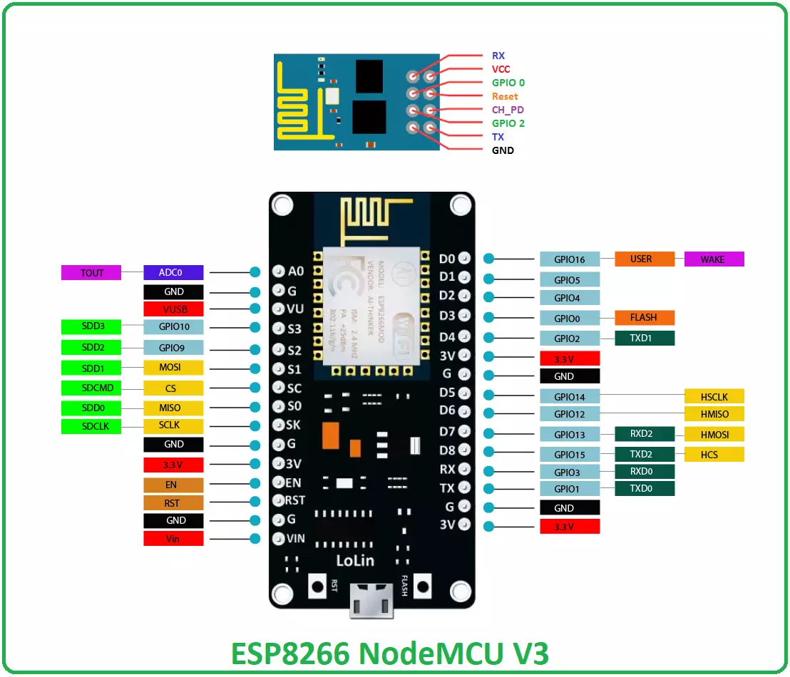
Hello friends! Hope you are doing well. Today, we will have a look at the detailed Introduction to ESP8266 WiFi module. ESP8266 is a very low-cost & user-friendly WiFi module, which develops a simple TCP/IP connection and can easily be interfaced with microcontrollers via Serial Port. The first chip in this series was ESP-01 which gained sheer attention in the market. In this tutorial, we will discuss the ESP8266 WiFi module along with its pinout, features, specifications, applications and datasheet. Let's dive in and nail down everything related to this device.

ESP8266 WiFi Module

  • ESP8266 (also called ESP8266 Wireless Transceiver) is a cost-effective, easy-to-operate, compact-sized & low-powered WiFi module, designed by Espressif Systems, that supports both TCP/IP and Serial Protocol.
  • It's normally used in IOT cloud-based embedded projects and is considered the most widely used WiFi module because of its low cost and small size.
  • It runs at an operating voltage of 3V and can handle a maximum voltage of around 3.6 V, so an external logic level converter is required if you are using 5V supply.
  • ESP8266 WiFi module can easily be interfaced with microcontrollers board (i.e. Arduino UNO) via Serial Port.
  • There are numerous breakout boards available based on ESP8266 WiFi Module (i.e. ESP8266 NodeMCU V3).
  • Beause of its compact size, its mostly used in autonomous projects (i.e. Robotics).
  • Other than ESP8266, "Espressif Systems" has designed many other ESP WiFi modules, few of them are shown in below figure:
Now let's have a look at the ESP8266 Pinout, necessary for interfacing with microcontrollers.

ESP8266 Pinout

  • ESP8266 Pinout consists of 8 pins in total, which are given in below table along with their operation:
ESP8266 Pinout
No. Pin Name Working
1 RX Serial Receiver Pin
2 Vcc Power Pin (+3.3 V; can handle up to 3.6 V)
3 GPIO 0 General-purpose I/O No. 0
4 RST Reset
5 CH_PD Chip power-down
6 GPIO 2 General-purpose I/O No. 2
7 TX Serial Transmitter Pin
8 GND Ground
  • Each pin comes with a specific function associated with it where Vcc and GND are voltage source and ground respectively.
  • RX and TX are used for communication where TX is dedicated for data transmission and RX is used receiving data.

ESP8266 Datasheet

  • You can download ESP8266 Datasheet by clicking the below button:
Download ESP8266 Datasheet

ESP8266 Features

  • It is also known as a system-on-chip (SoC) and comes with a 32-bit Tensilica microcontroller, antenna switches, RF balun, power amplifier, standard digital peripheral interfaces, low noise receive amplifier, power management module and filter capability.
  • The processor is based on Tensilica Xtensa Diamond Standard 106Micro and runs at 80 MHz.
  • It incorporates 64 KiB boot ROM, 80 KiB user data RAM and 32 KiB instruction RAM.
  • It supports Wi-Fi 802.11 b/g/n around 2.4 GHz and other features including 16 GPIO, Inter-Integrated Circuit (I²C), Serial Peripheral Interface (SPI), 10-bit ADC, and I²S interfaces with DMA.
  • External QSPI flash memory is accessed through SPI and supports up to 16 MiB and 512 KiB to 4 MiB is initially included in the module.
  • It is a major development in terms of wireless communication with little circuitry. and contains onboard regulator that helps in providing 3.3V consistent power to the board.
  • It supports APSD which makes it an ideal choice for VoIP applications and Bluetooth interfaces.

How to Power Up the Module

  • You can power up the device with PC port using USB to Serial adaptor. The 2 AA  and LIPO batteries are equally handy for powering up the device.
  • It is advised to not power this device directly with 5V dev board. Doing so can severely affect the quality and overall performance of the device.

ESP8266 NodeMCU

  • There are numerous breakout boards designed by different companies, based on this ESP8266 WiFi module.
  • Among these breakout boards, ESP8266 NodeMCU is the most popular one.
  • Here's the Pinout Diagram of ESP8266 NodeMCU:

ESP8266 Projects & Applications

ESP8266 WiFi module is widely used in embedded projects and thus brings WiFi capability. Here's few ESP8266 Projects & Applications:
  • Wireless Web Server
  • Geolocation using ESP8266
  • Pressure Sensors on Railway Tracks
  • Air Pollution Meter
  • Temperature logging system
  • World’s smallest IoT project
  • Wi-Fi controlled robot
  • Humidity and temperature monitoring
  • M2M using ESP8266
That's all for today. I hope I have given you everything you needed to know regarding this WiFi module. If you are unsure or have any question, you can ask me in the comment section below. I'd love to help you in any way I can. You are most welcome to keep us updated with your suggestions so we keep providing quality work that resonates with your needs and demands. Thanks for reading the article.

Rain Sensor Library for Proteus

Hello friends, I hope you all are doing great. In today's tutorial, I am going to share a new Rain Sensor Library for Proteus. I have got a lot of requests for designing this sensor. So finally it has been designed by our team and is ready to use in your Proteus Simulations. Rain Sensor, as the name shows, is used for detection of rain and is common sensor used in Embedded Systems Projects. Both analog and digital rain sensors are available these days but we have only designed the digital Rain Sensor. It will give digital output and its output will be HIGH when there's rain and will remain LOW if it won't detect any rain. As Proteus is a simulation software and we can't actually bring the rain so that's why I have placed a TestPin. If you apply HIGH to this TestPin then that's means there's rain and if TestPin is LOW then it will give LOW output and will show there's no rain. So, now let's have a look at How to download and use this Rain Sensor Library for Proteus:

Rain Sensor Library for Proteus

  • First of all, download this Rain Sensor Library for Proteus, by clicking the below button:
Rain Sensor Library for Proteus
  • You will get a zip file so extract it and you will find these three Library Files in it:
    • RainSensorsTEP.LIB
    • RainSensorsTEP.IDX
    • RainSensorsTEP.HEX
  • Now place these Library files in the Library folder of your Proteus software.
Note:
  • Now restart your Proteus software if its already open.
  • In the components search box, make a search for rain sensor as shown in below figure:
  • I have designed these two rain sensors so now place both of them in your workspace.
  • If everything goes fine then you will get something as shown in below figure:
  • So now we have to add the hex file in our sensor, so I am gonna use the Rain Sensor Blue and will double click it to open its Properties Panel.
  • In the Properties Panel, you have to find the Program File section.
  • In the Program File, browse to RainSensorsTEP.HEX File and select it.
  • We have download this file and placed it in the Library folder of our Proteus software.
  • Here's the screenshot of my Properties Panel of Rain Sensor:
  • Now after adding the Hex file, click OK to close the Properties Panel.
  • Your rain sensor is now ready to be used in your Proteus Simulation.
  • So, let's design a simple circuit to have a look at How this Rain Sensor works in Proteus.
  • Here's the screenshot of my simple Rain Sensor simulation in Proteus:
  • I have attached LogicState to TestPin and LED on the output.
  • As I have explained earlier that we can't bring rain in the Proteus software, that's why I have placed a TestPin.
  • So, now when TestPin is LOW that means there's no rain and when you change the TestPin to HIGH then sensor will detect rain.
  • I have run my simulation and here's the output:
So that was all for today. If you got into any trouble then ask in comments and I will help you out. Thanks for reading. Take care. :)

Introduction to RJ45

Hi Guys! Hope you are doing well. We always strive to give the most relevant information as per your needs and demands. Today, I'll discuss the details on the Introduction to RJ45. It is a type of standard connector mainly used for data transmission. Almost all ethernet cables come with this connector on each end, and they, sometimes, known as RJ cables. The RJ in the connector stands for registered jack while 45 defines the number of interface standard. In this post, I'll cover each and everything related to RJ45, why it used, features, and main applications. Let's dive right in and nail down everything you need to know.

Introduction to RJ45

  • RJ45 is a type of connector, mainly used for Ethernet networking including connection with PC network cards, data switches, WiFi access points, and routers.
  • It is connected to each end of Ethernet cables and acts as the main source for transferring data. RJ stands for registered jack and ethernet cables are also known as RJ cables.
  • The most common standard for RJ cables is known as CAT5 (Category 5)
  • In simple words, connectors at the end of ethernet cables are known as RJ45 connectors which also indicate how the cables are wired, while ethernet cables are termed as CAT5 (also RJ cables) which show the maximum speed the cable can attain.
  • RJ connector comes with eight pins which indicate it can house eight wires inside. All these wires come in different colors i.e four are in solid color while the remaining four are stripped. These wires are combined in twisted pairs that help in reducing the crosstalk and canceling EMI.
  • These cables are not shielded and are merely twisted for noise reduction.
  • CAT cables are mostly used in networking and can handle bandwidth around 100mbps.
  • These cables fail to work in high-speed environments, in that case, CAT5 is widely replaced by CAT6.
  • RJ45 cables deem feasible for both long and short distance, and apart from supporting ethernet protocol, they also work for ATM and serial ISDN T1 and E1.
  • RJ45 come with 8 wires and only 4 of them take part in the communication where pin 1 and 2 are used for data transmission while pin 3 and 4 are used for receiving data. (only in ethernet interface)
  • In serial and ISDN protocols, all pins take part in the communication and are wired in a straight through configuration.
  • Don't get confused between RJ connectors and RJ ports. Both are the part of RJ protocol where connectors serve as a (male) connector and port that receives the connector is known as (female) port.
 RJ45 Pinout and Wiring Standards
RJ cables are wired in two ways named T-568A and T-568B. Wiring standards in both of them are different and listed below.
  • Both wiring schemes are equally practiced and commonly supported by most of the devices, however, T-568A is preferred over other.
Following figure shows the pinout of RJ45 (T-568A). Following figure shows the pinout of the RJ45 (T-568B).
  • In some networking applications, crossover ethernet cable is a prerequisite which contains T-568B at one end and T-568A on the other end.
  • This cable is mainly used in computer-to-computer connections.
Difference between RJ45 and RJ11
  • Both connectors are different in terms of size, wires, and applications.
  • RJ45 is relatively large as compared to RJ11 and mainly used to build a connection with routers, computers, XBoxes, hardware firewalls and play stations. It comes with 8 wires.
  • While RJ11 is smaller in size, comes with 4 wires and mainly used for connection with telephone, modem, and fax machine.
  • Although RJ11 comes in smaller size and can fit in the RJ45 slot, however, it is not recommended to use this practice. Doing so can damage the slot and affect the overall working of the device in which it is plugged in.

Types of Ethernet Cables

Ethernet cables are widely used for telecommunication and networking purpose. They come in different types based on nature and data transmission speed they can carry along the length of the wire. RJ45 connectors are connected on both sides of the cables that act as a source of data transmission. Following are the main types of Ethernet cables used for networking and telecommunication purpose. CAT-1. It stands for category 1 that doesn't support TIA (telecommunication industries association). It is mainly used for standard telephone wiring and ISDN. CAT-2. Similar to CAT-1, this type of wiring is not recognized by TIA. It is mainly used for token ring wiring and capable of carrying data at the rate of 4Mbit/s. This is the old version of cable wiring and widely abandoned by advanced cable categories. CAT-3. This cable wiring is widely supported and recognized by TIA/EIA. It is mainly used for data networks and can carry data at the rate of 100Mbit/s. However, this type of wiring is also becoming obsolete because of less data transmission speed and frequency for carrying out different functions at the decent pace. CAT-4. This type of cable wiring is not supported by TIA. It is widely used for token ring networks with the capability of supporting frequency up to 20MHz. CAT-5. Category 5 cables were introduced with the intention of providing more speed as compared to their predecessors. They can transmit frequency up to 100MHz and are not recognized by TIA. This cable wiring uses two twisted pair and is not recognized by TIA. The CAT-5 cable is not recommended for recent applications, however, it is useful for 100Base-T and 1000Base-T networks as it provides suitable speed and frequency for the data networks. CAT-5e. This cable wiring is almost similar to CAT-5 with some exemptions in terms of data transmission speed and TIA recognition. It is preferred for applications where speed is a major concern as it can support speed up to 125 Mbps. The physical appearance of this wiring is similar to CAT-5 and widely used for 100Base-T and 1000Base-T networks. CAT-6. This cable wiring is recognized by TIA and stays ahead of other ethernet cables in terms of performance and speed i.e. supports up to 10Gbps. They come with an outer foil or braided shielding and cover less space as they are tightly wound as compared to CAT-5 and CAT-5e. The shielding minimizes the crosstalk and noise and protects the twisted pair of wires inside the cable. They can work and cover a distance of around 55 meters. CAT-6a. It stands for Category 6 Augmented cable. They come with higher transmission speed, encompass maximum bandwidth and are less flexible than CAT-6 cables. They can carry more data along the length of the cable as compared to their predecessors and cover more distance without losing the bit of accuracy. The shielding is added in the wiring that protects the cable and helps in removing the crosstalk. CAT-7. It supports frequency up to 600 Mbps and comes with four individually shielded pairs. It works best in many applications for carrying out data transmission at a decent pace. They are introduced for rated speed of around 10 Gigabit. CAT-7a. These cables are used for augmented specifications that can support speed around 10 Gigabit. They cover frequency up to 1000 MHz and are quite identical to CAT-7 cables in terms of physical appearance and performance capability.

How to Connect Two Computers Using Ethernet Cables

It is very easy to connect two computers for data transmission using ethernet cables. The CAT-5 or CAT-5e crossover cables are widely used for this purpose and prevent from losing any data during transmission. These cables are quite identical to straight through cables but come with twisted wires on both ends. You can use the following steps to connect two computers using ethernet cables.
  • Connect one end of the cable with RJ45 connector into the ethernet port of the computer. Plug the other end of the cable into another computer.
  • Log in to one of the computers.
  • Go to the search box at the bottom left of the computer and type "Network and Sharing Center" and click it.
  • Then go to the "Change Adaptor Settings" on the top left side.
  • Right click on the "Ethernet" and go to properties.
  • Then select "Internet Protocol version 4 TCP/IPv4" and click properties.
  • Select the IP address and subnet mask at the two computers as mentioned below.
To check the connection, restart both PC and use the below instructions.
  • ping 192.168.0.2 -t: from the second PC
  • ping 192.168.0.1 -t: from the first PC
Right click on this PC option and click on "Change Settings" option.
  • The "Workgroup" name should be identical in both PC, otherwise, ethernet connection won't work.
  • If you want to share whole drive, just right click on the drive you want to share and select share with "Advanced Sharing Options" and check the box beside share this folder option and click "OK" to apply changes.
Applications
  • RJ45 are mainly used in ethernet cables for data transmission. They come in two types i.e. T-568A and T-568B.
  • As compared to the RJ11 connector, RJ45 comes with more applications including ethernet networking, industrial automation, and telecommunications.
That's all for today. I hope I have given you everything you need to know about RJ45. However, if you are feeling skeptical or have any question, you can approach me in the comment section below. I'd love to help you in any way I can. Feel free to keep us updated with your valuable feedback and suggestions, they help us provide you quality work so you keep coming back for what we have to offer. Thanks for reading the article.

Solar Panel Library for Proteus

Hello friends, I hope you all are doing great. In today's tutorial, I am going to share a new Solar Panel Library for Proteus. I hope you guys are gonna enjoy this Proteus Library as it's not available in Proteus and we are presenting it for the first time. :) I am quite proud of my team. B| We all know about Solar Panels which is an excellent renewable energy source. It is widely adopted by the inhabitants of this green planet as its totally free and converts solar energy into electricity. Solar panels are also used a lot in Engineering Projects especially related to renewable energy sources. Proteus doesn't have solar panels in its database that's why our team has designed this library. Using this Solar Panel Library for Proteus, now you can easily simulate solar panels in Proteus and can design your projects' simulations. I will also share some projects in which I will interface it with different Microcontrollers like Arduino, PIC Microcontroller or 8051 Microcontroller etc. So, let's get started with How to download and simulate Solar Panel in Proteus:

Solar Panel Library for Proteus

  • First of all, download the Solar Panel Library for Proteus by clicking the below button:
Solar Panel Library for Proteus
  • You will get a zip file which will have these two library files in it:
    • SolarPanelTEP.IDX
    • SolarPanelTEP.LIB
  • Now place these two files in the library folder of your Proteus software.
Note:
  • Now open you Proteus software or restart it if it's already open.
  • Proteus is not that smart so we have to restart it so that it would add new Library components in its database.
  • In the Proteus software click on the components button and make a search for Solar Panel as shown in below figure:
  • Now place this component in your Proteus software.
  • If everything goes fine then you will get something as shown in below figure:
  • Now double click this solar panel and its Properties panel will open up as shown in below figure:
  • If you have worked on Solar Panel then must have the idea that output of solar panel depends on the intensity of sunlight.
  • So, if its shiny bright day then solar panel normally give in the range of 15V to 19V.
  • Similarly, if its night time then solar panels output ranges from 2V to 6V.
  • While on a cloudy day it could vary between 8V to 12V.
  • So, if you want to change the output of this Proteus' Solar Panel then you have to open this Properties Panel and then change the Voltage value.
  • By default, it will give 12V as an output.
  • I am working on adding some button so that you could change the output in running simulation but for now you have to stop the simulation in order to change it.
  • Now let's place a voltmeter at the output of this solar panel and check its output.
  • Here's the simple solar panel simulation in Proteus:
  • Now you can see in above figure that our Solar Panel is giving 12V as an output.
  • So, now let's open it's Properties Panel and change the voltage value to 16.5V.
  • I have changed the value and here's our output:
  • You can see in the above figure that now voltage has changed to 16.5V.
  • Here's a video demonstration on How to download and install this Solar Panel Library for Proteus.
So, that was all about Solar Panel Library for Proteus. I hope you guys can now easily download and install it. If you still got in to any trouble then ask in comments and I will try my best to resolve them and also let me know about your feedback for this Library. Thanks for reading. Have a good day. :)

Infrared Sensor Library for Proteus

Hello friends, I hope you all are doing great. In today's tutorial, I am going to share a new Infrared Sensor Library for Proteus. This IR sensor is not available in Proteus and we are sharing this library for the first time. I hope it will help in your Embedded Systems Projects particularly related to robotics and automation. So, if you want to work on this IR Sensor then I would suggest you to first design its simulation and then try your luck with hardware. There are different types of Infrared Sensors & modules available in the market. Some of these modules have transmitter & receiver on separate chips and are mostly get activated when someone interrupts the light. The one we have designed has a transmitter & receiver on a single chip. The IR signal transmits from the IR transmitter and if it has some obstacle in front of it then it bounces back and received by the IR receiver. You should also have a look at this list of New Proteus Libraries for Engineering Students. So, let's have a look at How to use this Infrared Sensor Library for Proteus: Note:
Where To Buy?
No.ComponentsDistributorLink To Buy
1Arduino UnoAmazonBuy Now

Infrared Sensor Library for Proteus

  • First of all, download the Library files of this IR Sensor by clicking the below button:
Infrared Sensor Library for Proteus
  • After downloading this file extract it and you will find three Library files in it, named as:
    • InfraredSensorsTEP.IDX
    • InfraredSensorsTEP.LIB
    • InfraredSensorsTEP.HEX
  • Place all these three files in the Library folder of your Proteus software.
Note:
  • Once you have added the files in the Library folder, then restart your Proteus software.
  • In the components section, make a search for Infrared Sensor, as shown in below figure:
  • Now place this IR Obstacle Sensor in your Proteus and if everything goes fine then you will get something as shown in below figure:
  • As you can see in above figure that we have four pins on our Infrared sensor, which are:
    • Vcc => You need to provide +5V to this pin.
    • GND => It should be grounded.
    • OUT => That's output pin and it will get HIGH when this sensor will find some obstacle in front and will remain LOW in normal condition.
    • TestPin => As Proteus is a simulation software so we can't actually place something in front of this sensor. That's why I have used this TestPin. If this Pin is LOW, then sensor will remain normal and if it's HIGH then sensor will behave as it has something in front of it.
  • Now double click this Infrared Sensor and its Properties Panel will open up.
  • In the Program File section, browse to the file InfraredSensorTEP.HEX which you have already downloaded and placed in the Library folder of Proteus.
  • Here's the screenshot of Properties Panel for this Infrared Sensor:
  • I have encircled the Program File in above figure and you can see I have selected the InfraredSensorsTEP.HEX.
  • So, now let's design a simple circuit and have a look at how to use this Infrared Sensor in Proteus.
  • Here's the screenshot of Infrared Sensor Simulation in Proteus:
  • So, now let's run our Proteus simulation and if everything goes fine then you will get results, as shown in the below figure:
  • I will interface this sensor with different Microcontrollers e.g. Arduino, PIC Microcontroller etc. in my coming tutorial.
  • As you can see in the above figure that when TestPin is LOW then OUT Pin is also LOW means there's no obstacle and when TestPin gets 1 then OUT Pin will go HIGH and that means we have some obstacle.
So, that's all for Infrared Sensor Library for Proteus. I hope it will help you guys in your engineering projects. Let me know if you have any suggestions. Take care & have fun !!! :)

Introduction to Arduino Mega 2560

Hey Fellas! Hope you are doing well. Today, I am going to unlock the details on the Introduction to Arduino Mega 2560. It is a microcontroller board based on Atmega 2560 microcontroller. Arduino Boards have revitalized the automation industry with their easy-to-use platform where everyone with little or no technical background can get started with learning some basic skills to program and run the board.

I have updated articles previously on Arduino Uno, Arduino Nano, and Arduino Pro Mini. All these boards function similarly in one way or the other. There are some basic features like PCB layout design, size, number of analog pins and breadboard friendly nature that make them different from each other. In terms of coding, all these boards are programmed in Arduino IDE software and you don't need to attach extra components or devices to put them in running condition. Everything is already built in the board that makes this device readily available. Just plug and play with the board as per your requirement. Here's the video presentation of Arduino Mega 2560:

All the boards mentioned above work perfectly for a number of Arduino Projects when you require a simple task to be completed with fewer I/O pins and memory. However, when the project goes complex, a board with less memory fails to complete the task. This is where Arduino Mega 2560 comes in handy. This board comes with 54 pins and 16 analog pins with more memory to store the code. Sounds crazy, isn't it? Thanks to technology that keep your covered in every aspect and provides support in any way when it comes to fulfilling your technical needs.

I'll try to cover each and everything related to Arduino Mega 2560, what is this about, the main features, working, technical specifications and everything you need to know. Let's jump right in.

No. Pin Number Pin Description
1 D0 - D53 54 Digital Input / Output Pins.
2 A0 - A15 16 Analog Input / Output Pins.
3 D2 - D13 12 Pulse Width Modulation ( PWM ) Pins.
4 Pin # 0 (RX) , Pin # 1 (TX) Pin # 19 (RX1) , Pin # 18 (TX1) Pin # 17 (RX2) , Pin # 16 (TX2) Pin # 15 (RX3) , Pin # 14 (TX3)  4 Serial Communication Ports (8 Pins).
5 Pin # 50 ( MISO ) Pin # 51 ( MOSI ) Pin # 52 ( SCK ) Pin # 53 ( SS ) SPI Communication Pins.
6 Pin # 20 ( SDA ), Pin # 21 ( SCL ) I2C Communication Pins.
7 Pin # 13 Built-In LED for Testing.
Other Arduino Boards:
You should also have a look at these other Arduino board, you might find them interesting as well. Compare their features and find the most suitable one for your project. Here's the list of other Arduino boards:
Where To Buy?
No.ComponentsDistributorLink To Buy
1Arduino Mega 2560AmazonBuy Now

Introduction to Arduino Mega 2560

  • Arduino Mega 2560 is a Microcontroller board based on Atmega2560. It comes with more memory space and I/O pins as compared to other boards available in the market.
  • There are 54 digital I/O pins and 16 analog pins incorporated on the board that make this device unique and stand out from others.
  • Out of 54 digital I/O, 15 are used for PWM (pulse width modulation).
  • A crystal oscillator of 16MHz frequency is added on the board.
  • This board comes with USB cable port that is used to connect and transfer code from computer to the board.
  • DC power jack is coupled with the board that is used to power the board. Some version of the Arduino board lacks this feature like Arduino Pro Mini doesn't come with DC power jack.
  • ICSP header is a remarkable addition to Arduino Mega which is used for programming the Arduino and uploading the code from the computer.
  • You can download the Arduino Mega 2560 datasheet bu clicking below button:
Download Arduino Mega 2560 Datasheet
  • This board comes with two voltage regulator i.e. 5V and 3.3V which provides the flexibility to regulate the voltage as per requirements as compared to Arduino Pro Mini which comes with only one voltage regulator.
  • There is no much difference between Arduino Uno and Arduino Mega except later comes with more memory space, bigger size and more I/O pins.
  • Arduino software called Arduino IDE is used to program the board which is a common software used for all boards belonged to Arduino family.
  • Availability of Atmega16 on the board makes it different than Arduino Pro Mini which uses USB to serial converter to program the board.
  • There is a reset button and 4 hardware serial port called USART which produces a maximum speed for setting up communication.
  • The following figure shows the specifications of Arduino mega 2560.
  • Arduino Mega is specially designed for the projects requiring complex circuitry and more memory space. Most of the electronic projects can be done pretty well by other boards available in the market which make Arduino Mega uncommon for regular projects. However, there are some projects that are solely done by Arduino Mega like making of 3D printers or controlling more than one motors, because of its ability to store more instructions in the code memory and a number of I/O digital and analog pins.
  • There are three ways to power the board. You can either use a USB cable to power the board and transfer code to the board or you can power it up using Vin of the board or through Power jack or batter.
  • Last two sources to power the board are required once you already built and compile code into the board through USB cable.
  • This board comes with resettable polyfuse that prevents the USB port of your computer from overheating in the presence of high current flowing through the board. Most of the computers come with an ability to protect themselves from such devices, however, the addition of fuse provides an extra layer of protection.
  • It can be used either way i.e. for creating stand-alone projects or in combination with other Arduino boards. Most complex projects can be created using this board.
Let's have a look at Arduino Mega 2560 Pinout:

Arduino Mega 2560 Pinout

  • Following figure shows the pinout of Arduino Mega 2560:
  • Each pin comes with a specific function associated with it. All analog pins can be used as digital I/O pins.
  • Designing of a project using Arduino Mega gives you the flexibility of working with more memory space and processing power that allows you to work with a number of sensors at once. This board is physically larger than other Arduino boards.

Arduino Mega 2560 Pin Description

  • 5V & 3.3V. This pin is used to provide output regulated voltage around 5V. This regulated power supply powers up the controller and other components on the board. It can be obtained from Vin of the board or USB cable or another regulated 5V voltage supply. While another voltage regulation is provided by 3.3V pin. Maximum power it can draw is 50mA.
  • GND. There are 5 ground pins available on the board which makes it useful when more than one ground pins are required for the project.
  • Reset. This pin is used to reset the board. Setting this pin to LOW will reset the board.
  • Vin. It is the input voltage supplied to the board which ranges from 7V to 20V. The voltage provided by the power jack can be accessed through this pin. However, the output voltage through this pin to the board will be automatically set up to 5V.
  • Serial Communication. RXD and TXD are the serial pins used to transmit and receive serial data i.e. Rx represents the transmission of data while Tx used to receive data. There are four combinations of these serial pins are used where Serail 0 contains RX(0) and TX(1), Serial 1 contains TX(18) and RX(19), Serial 2 contains TX(16) and RX(17), and Serial 3 contains TX(14) and RX(15).
  • External Interrupts. Six pins are used for creating external interrupts i.e interrupt 0(0), interrupt 1(3), interrupt 2(21), interrupt 3(20), interrupt 4(19), interrupt 5(18). These pins produce interrupts by a number of ways i.e. providing LOW value, rising or falling edge or changing value to the interrupt pins.
  • LED. This board comes with built-in LED connected to digital pin 13. HIGH value at this pin will turn the LED on and LOW value will turn it off. This gives you the change of nursing your programming skills in real time.
  • AREF. AREF stands for Analog Reference Voltage which is a reference voltage for analog inputs.
  • Analog Pins. There are 16 analog pins incorporated on the board labeled as A0 to A15. It is important to note that all these analog pins can be used as digital I/O pins. Each analog pin comes with 10-bit resolution. These pins can measure from ground to 5V. However, the upper value can be changed using AREF and analogReference() function.
  • I2C. Two pins 20 and 21 support I2C communication where 20 represents SDA (Serial Data Line mainly used for holding the data) and 21 represents SCL(Serial Clock Line mainly used for providing data synchronization between the devices)
  • SPI Communication. SPI stands for Serial Peripheral Interface used for the transmission of data between the controller and other peripherals components. Four pins i.e. 50 (MISO), 51 (MOSI), 52 (SCK), 53 (SS) are used for SPI communication.

Arduino Mega 2560 Dimensions

Follwoing figure shows the dimensions of the Arduino Mega 2560:
  • Arduino Mega is comparatively larger than other boards available in the market. It comes 4-inch length and 2.1-inch width. However, USB port and power jack are slightly extended from the given dimensions.

Shield Compatibility with Arduino Mega 2560

  • Arduino Mega is compatible with most of the shields designed for other Arduino boards.
  • Before you intend to use a shield, make sure the operating voltage of the shield is compatible with the board voltage. Most of the shields operate at 3.3V or 5V which is compatible with this board, however, shields with higher operating voltage can damage the board.
  • Also, the header distribution of the shield must resonate with the pin distribution of the board, so you can simply attach the shield with the board and make it in a running condition.

Arduino Mega 2560 Programming

  • Arduino Mega 2560 can be programmed using Arduino Software called IDE which supports C programming.
  • The code you make on the software is called sketch which is burned in the software and then transferred to the board through USB cable.
  • This board comes with a built-in bootloader which rules out the usage of an external burner for burning the code into the board.
  • The bootloader communicates using STK500 protocol.
  • Once you compile and burn the program on the board, you can unplug the USB cable which eventually removes the power from the board. When you intend to incorporate the board into your project, you can power it up using power jack or Vin of the board.
  • Multitasking is another feature where Arduino mega comes handy. However, Arduino IDE Software doesn't support multitasking feature but you can use other operating systems like FreeRTOS and RTX to write C program for this purpose. This gives you the flexibility of using your own custom build program using ISP connector.

Arduino Mega 2560 Applications

Arduino Mega 2560 is an ideal choice for the projects requiring more memory space to used with more number of number pins on the board. Following are the main applications of the Arduino mega boards.
  • Developing 3D printer
  • Controlling and handling more than one motors
  • Interfacing of number of sensors
  • Sensing and detecting temperature
  • Water level detection projects
  • Home automation and security systems
  • Embedded Systems
  • IoT applications
  • Parallel programming and Multitasking
That's all for today. I hope you have found this article useful. However, if you are unsure or have any question you can ask me in the comment section below. I'd love to help you according to best of my expertise. Feel free to keep us updated with your feedback and suggestions, they help us provide you quality work that resonates with your field of work and helps you keep coming back for what we have to offer. Thanks for reading the article.

Introduction to Arduino Pro Mini

Hey Friends! Hope you are doing well. Today, I am going to give you a detailed Introduction to Arduino Pro Mini. It's a microcontroller board developed by Arduino.cc and is based on the Atmega328 microcontroller.

Arduino Pro Mini is quite similar to Arduino UNO in overall functionality however the main difference lies in its size and built-in programmer. Arduino Pro Mini is very small in size & it lacks a built-in programmer & USB Port. Arduino Uno comes with two onboard voltage regulators (i.e. 5V and 3.3V) while Arduino Pro Mini comes with a single voltage regulator.

There are two versions of Arduino Pro Mini available, first one operates at 5V & runs at 16MHz while the second one is of 3.3V runs at 8MHz.

Arduino boards are mainly used for the development of automation, robotics, embedded systems and other electronics projects. These boards were developed with the intention of providing easy hardware and software combination that gives a quick pathway to people with no technical background.

Arduino Pro Mini Key Features
No. Feature Value
1 Microcontroller ATmega328
2 Operating Frequency/Crystal Oscillator 16MHz/8MHz
3 Digital I/O Pins 14
4 Analog Pins 8
5 PWM(Pulse Width Modulation) Pins 6
6 Built-in Programmer Not available.
7 USB Port Not available.
8 Flash Memory 32KB
9 SRAM 2KB
10 EEPROM 1KB
11 Bootloader 0.5KB in Flash Memory.
In today's tutorial, I'll discuss each and everything related to Arduino Pro Mini so you don't need to scrape through the internet and find all information in one place. Let's get started.
Where To Buy?
No.ComponentsDistributorLink To Buy
1Arduino Pro MiniAmazonBuy Now

Introduction to Arduino Pro Mini

  • Arduino Pro Mini is a compact, small-sized & application-type microcontroller board, developed by Arduino.cc and comes with an Atmega328 microcontroller incorporated on the board.
  • This board comes with 14 Digital I/O Pins, out of which 6 pins are used for providing PWM output.
  • Arduino Pro Mini Pinout also consists of 8 Analog Pins.
  • The size of Arduino Pro Mini is 1/6th of the size of Arduino Uno, so it's quite small as compared to Arduino UNO.
  • Depending on operating voltage, Arduino Pro Mini is of two types:
    1. Operating Voltage: 5.0V, Crystal Oscillator: 16MHz, Voltage Regulator: KB33.
    2. Operating Voltage: 3.3V, Crystal Oscillator: 8MHz, Voltage Regulator: KB50.
  • In order to reduce the size, the USB port & built-in programmer are removed from Arduino Pro Mini, so after uploading code you can simply place it in your application(that's why also termed as application-type).
  • Official Arduino Software called Arduino IDE (Integrated development environment) is used to write & upload programming code. The code we write to program this board is normally called a sketch.
  • Arduino Pro Mini also has a Reset Button and a small LED connected to pin number 13.

Arduino Pro Mini Memory Allocations

  • Arduino Pro Mini comes with 3 types of built-in memories:
    1. Flash Memory of 32KB out of which 0.5KB is used by the bootloader code.
    2. SRAM of 2KB.
    3. EEPROM of 1KB.
Now let me give you a brief overview of these memories, I have explained them in detail here: What is a Microcontroller?
  • Flash Memory is a non-volatile memory and is used for storing the programming code. As it's a non-volatile memory so it stores information even if the connection with the power supply is lost.
  • SRAM(Static Random Access Memory) usually referred to as RAM memory is a volatile memory and is used to store temporary data i.e. variables. It loses data if we cut off the power supply.
  • EEPROM is a semi-volatile memory and thus can be erased by programming.

Arduino Pro Mini Specifications

Here, I have shared a few more specifications and functionalities of Arduino Pro Mini.
  • This board doesn't come with connectors already soldered which gives you the flexibility to solder the connectors in any way you want, based on the requirements and space available for your project.
  • There is only one voltage regulator incorporated on the board i.e 3.3V or 5V based on the version of the board.
  • The labeling on the voltage regulator defines the version of the board i.e. KB33 represents 3.3V edition and KB50 represents 5V edition. However, the board version can also be indicated by measuring the voltage between Vcc and GND pin.
  • Overcurrent protection is another feature available in Arduino Pro Mini.
  • The following figure shows the specifications of the board.

Arduino Pro Mini Datasheet

  • You can download Arduino Pro Mini Datasheet by clicking the below button:
Download Arduino Pro Mini Datasheet Now let's have a look at the Pinout of Arduino Pro Mini in detail:

Arduino Pro Mini Pinout

  • As we know, each pin of the Microcontroller is assigned with multiple functions.
  • In the below table, I have shared the key points of the Arduino Pro Mini pin diagram and labeled functions assigned to them:
Arduino Pro Mini Pinout
No. Pin Number Pin Description
1 Pins 0 - 13 14 Digital I/O Pins.
2 Pins A0 - A7 8 Analog Pins.
3 Pins 3, 5, 6, 9, 10 & 11 6 Pulse Width Modulation ( PWM ) Pins.
4 Pins 0(RX) & 1(TX) Serial Communication Pins.
5 Pins 10, 11, 12 & 13 SPI Communication Pins.
6 Pins A4 & A5 I2C Communication Pins.
7 Pin # 13 Built-In LED for Testing.
8 Pins 4 & 5 External Interrupt Pins.
  • Here's the Circuit Diagram of Arduino Pro Mini Pinout:

Arduino Pro Mini Power Pins

  • Vcc: Arduino Pro Mini Pinout consists of 2 Vcc Pins. It gives the regulated voltage i.e. 5V or 3.3V depending on the type of the board.
  • GND: There are 3 GND(ground) pins incorporated on the board.
  • RAW. This pin is used for supplying raw voltage to the board. You can power connect an external power supply ranging from 5V to 12 V.
  • Reset: Pro Mini board comes with 2 Reset Pins, which comes in handy if the board hangs up in the middle of the running program, making this pin LOW will reset the board.
  • In the below figure, I have highlighted the Power Pinout of Arduino Pro Mini:

Programming Header Pins

  • Programming Header: FTDI six-pin programmer is connected with these pins and is used to upload programming code on the Pro Mini board.

Arduino Pro Mini I/O Pins

  • Digital Pins: Arduino Pro Mini has 14 Digital I/O Pins in total labeled from 0 to 13, where Pin 0 is RX1 and Pin 1 is TX0.
  • Analog Pins: It has 8 analog pins labeled from A0 to A7. These pins are used to input analog signals and come with a total resolution of 10bit.
I have encircled digital pins with green color and analog pins with orange color in the below figure:

Arduino Pro Mini Communication Pins

  • Arduino Pro Mini supports 3 Communication Protocols for the transmission of data with other peripherals i.e. sensors, registers etc. and are named as:
    1. Serial Protocol.
    2. I2C Protocol.
    3. SPI(Serial Peripheral Interface) Protocol.
  • TXD & RXD Pins: These pins are used for serial communication. TXD represents the transmission of serial data while RXD is used for receiving the data. Code is also uploaded through Serial Protocol.
  • SPI Pins: Four pins 10(SS), 11(MOSI), 12(MISO), and 13(SCK) are used for communicating through SPI Protocol.
  • I2C Pins: Two Pins(A4 and A5) are used for developing I2C communication. A4 is known as serial data line (SDA) which holds the data and A5 shows serial clock line (SCL) which provides data synchronization clock.

Other Pinouts

  • PWM. There are 6 digital pins labeled as 3,5,6,9,10, and 11 available on the board that provide PWM (pulse width modulation).
  • External Interrupts. There are two external interrupts available called T0(at Pin 4) and T1(at Pin 5). They are also known as hardware interrupts.

Arduino Pro Mini Vs Other Arduino Boards

  • Most of the Arduino boards come with a USB port that is used to send the program from the computer to the board. However, in the case of Arduino Pro Mini, all of the USB circuitry is removed to make it as compact and small as possible. You can program the board using a USB to serial converter cable. The FT232RL USB serial module is very handy and preferable for programming this board. A six-pin FTDI header can be connected to a USB to serial converter that provides the USB power.
  • If you have already worked on the Arduino Uno board, then no need to buy a USB to serial converter cable as you can program the Pro Mini using Uno board. Make sure, the Pro Mini version you are working on comes with 5V regulation as it runs at 16MHz like Arduino Uno board. Programming your 3.3V Pro Mini board will not be compatible with the Arduino Uno board, hence making it very difficult to program the 3.3V version of the Pro Mini board.
  • The form factor is another major difference that makes this device unique.
  • Pro Mini comes in a very small and compact size which makes this device suitable for most applications. But small size comes with one limitation i.e. it doesn't compatible with Arduino Shields unless you hard-wire the board with Arduino Shield.

Arduino Pro Mini Set Up

  • First, you need to install the Arduino IDE software on your computer, which is the official software used to program Arduino boards.
  • Connect the board with USB to Serial converter (FTDI serial module) that is used to transfer the program from computer to the board.
  • Write the program in the IDE software in C language.
  • No separate burner is required to burn the code. You can directly burn the code in the IDE software and transfer it to the board.
  • Once you have burned and transferred the program to the board, the next step is to power the board to make it compatible with your project.
  • Apart from using FTDI serial module, there are two ways to power the board. You can power the board through the RAW by setting the voltage range anywhere between 5V to 12V. It will automatically regulate to 3.3V based on the version of the board. However, if your project comes with a regulated voltage of 3.3V, then you can connect it directly to the Vcc pin of the board. Make sure, the board version is KB33 that runs at 3.3V, another version KB50 will run at 5V.
  • These two ways of powering up the board are useful when you have disconnected the board with the computer and already burned the program using FTDI module.

Applications of Arduino Pro Mini

There are many applications of Arduino Boards, but the small size and ease of use make Arduino Pro Mini stand out from others, especially where space requirement of the project is highly concerned. That's all for today. We always strive to give you quality work based on your needs and requirements. However, if you are unsure or have any question, you can approach me in the comment section below. I'd love to help you according to best of my knowledge. Keep your suggestions coming; they help us provide you best content so you keep coming back for what we have to offer. Thanks for reading the article.
Syed Zain Nasir

I am Syed Zain Nasir, the founder of <a href=https://www.TheEngineeringProjects.com/>The Engineering Projects</a> (TEP). I am a programmer since 2009 before that I just search things, make small projects and now I am sharing my knowledge through this platform.I also work as a freelancer and did many projects related to programming and electrical circuitry. <a href=https://plus.google.com/+SyedZainNasir/>My Google Profile+</a>

Share
Published by
Syed Zain Nasir