Hello friends, I hope you all are doing great. In today's tutorial, we will have a look at How to use Voltmeter & Ammeter in Proteus ISIS. It's our 4th tutorial in Proteus series. While designing an electronics project, voltage & current measurements are essential debugging features, as they help in understanding circuit behavior.
Proteus has builtin instruments for voltage & current measurement. We have have their probes and today we will discuss them in detail. First have a look at Voltmeter in Proteus ISIS:
How to use Voltmeter in Proteus ISIS
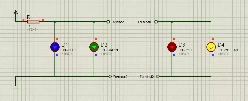
DC Voltmeter is used to measure the voltage difference across any DC component.
In order to use DC Voltmeter, we need to click on Virtual Instrum ...
Hello friends, hope you all are fine and having fun with your lives. Today's post is about How to increase Workspace in Proteus. It's our 3rd tutorial in Proteus series. Its quite a simple tutorial and along with this trick, I will also share few commonly used features or Proteus. Once, I was working on a simulation project in which I have to design a complete load management system in Proteus and it was quite messy as I have to include a lot of components and the area of Proteus got quite small for that and then I encountered this problem i.e. where to place the components.
You have seen in Proteus software that there's a blue rectangle which is considered as the workspace in Proteus. This area is constant and doesn't increase or decrease on its ...
Hello friends, I hope you all are doing great. In today's tutorial, we will simulate our First Electronics Project in Proteus ISIS. It's our 2nd tutorial in Proteus series. In our previous tutorial, we have seen a basic Introduction to Proteus and today, we will design a simple electronics circuit in it and will also simulate it.
If you want to work on Proteus, then you must have some prior knowledge about electronics. Proteus doesn't provide any suggestion about circuit designing so if you don't have electronics knowledge then you can't work with Proteus. Throughout this series, I will keep on explaining electronics circuits as well and will also embedded related components' links. So, if you are new to electronics then no need to worry and just ...
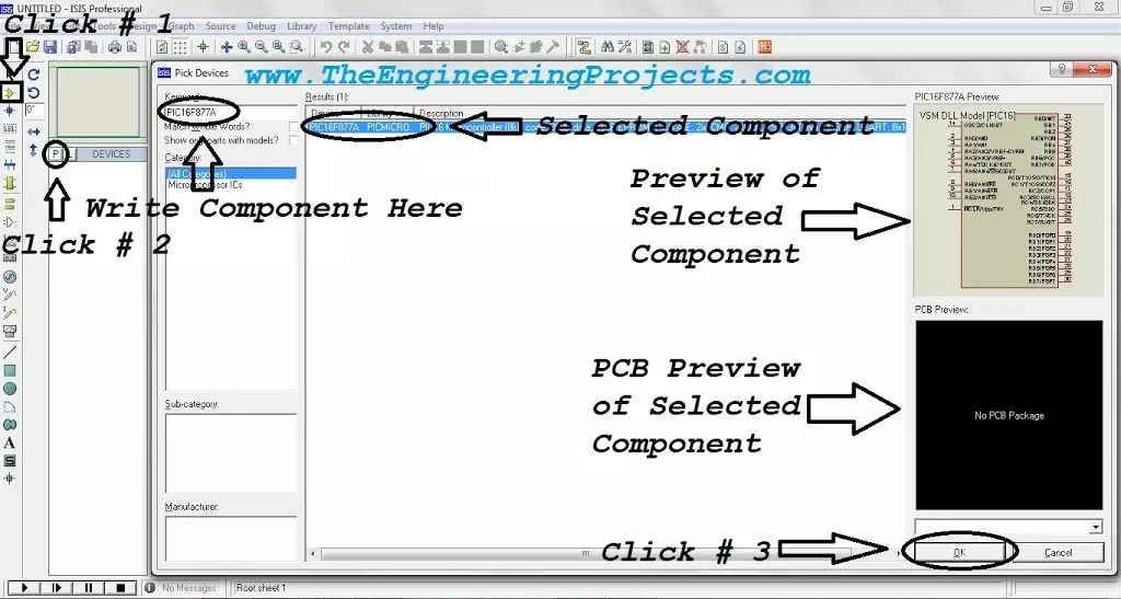
Hello readers, I hope you all are doing great. In today's tutorial, I am going to share a detailed Introduction to Proteus. It's our first tutorial in Proteus series. Today's tutorial is for beginners but still I would suggest you to read it once, as I am going to explain why Proteus?
Throughout our Engineering Course, we have to design a lot of electronics or embedded circuits and it's always a best approach to simulate these circuits first on some simulation software i.e. Proteus, PSPice etc., before assembling them on actual hardware. Among these simulation software, Proteus is my favorite one so let's get started with detailed Introduction to Proteus:
Introduction to Proteus ISIS
Proteus Design Sui ...
Hello friends, I hope you all are doing great. In today’s tutorial, we will have a look at Introduction to ADC0804. In electronic engineering different modules used to conversion of analog signal into a digital signal. These tools are recognised as analog to digital converter or ADC. Thes signal converter also used to find the value of input current and voltage. Normally the output of these converters are 2 binary numbers but other values are also possible. These analog to digital converter are available in different structure scheme but mostly they are available in integrated circuits packaging.
The working ability of these signal converter depends on their bandwidth and signal to noise ration (SNR). Their bandwidth can be fined by their sample r ...
Hello friends, I hope you all are doing great. In today’s tutorial, we will have a look at Introduction to STM32 Microcontroller. This microcontroller is a new category of a microcontroller family it is a thirty-two-bit microcontroller also compatible with the ARM and Cortex M processor. Due to thirty-two bits compatibility, this module provides good performance, processing of digital signal and consumes less power and voltage. The modules used in most of the industries due to their compatibility with the cortex M0, M0+, M3, M4.
In today's post, we will have a look at its working, features, pinouts, applications and some other related parameters. So lets with the Introduction to STM32 Microcontroller.
Introduction to STM32 Microcontroller
The STM32 is a type of microcontrolle ...
Hello friends, I hope you all are doing great. In today’s tutorial, we will have a look at Introduction to PT2272. It is a CMOS (complementary metal-oxide-semiconductor) that use to design simple wireless controlling of instruments installed at some distance. This module is normally used for controlling the circuits of garage door, speed control of the fan, robots and for monitoring the alarm connected at different places for security purposes.
This integrated circuitry uses non-variable code address and no built-in encryption due to these parameters it not used for such circuits where high security is need but uses only for small or less cost security circuits such as used in home security alarms etc. In today's post, we will have a look at its w ...
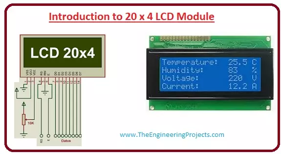
Hello friends, I hope you all are doing great. In today’s tutorial, we will have a look at the Introduction to 20x4 LCD Module. The LCD stands for liquid crystal display, which works on the light modulation features of liquid crystals. It is available in electronic visible display, video display and flat panel display. There are numerous categories and features are exist in markets of LCD and you can see it on your mobile, laptop, computer and television screen.
The invention of LCD gives new life to electronic industries and replaces lED and gas plasma techniques. It also replaces the CTR (cathode ray) tube that is used for visual display. The input power consumed by the liquid crystal display is less than the light-emitting diode and plasma display. In today's post, we will have a loo ...
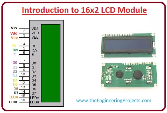
Hello friends, I hope you all are doing great. In today’s tutorial, we will have a look at Introduction to 16x2 LCD Module. LCD stands for liquid crystal display it is mostly used in different electronic projects and devices to display different values. LCD uses liquid crystals for the generation of visible images. 16 x 2 liquid crystal display is a basic LCD module used in DIY electronic projects and circuits. In this LCD module, there are two rows every row consists of sixteen numbers.
With the two rows in this module, there are sixteen columns. The VA dimensions of these modules are (66 x 16) millimeters and the thickness is 13.2 millimeters. Its operating voltage is plus five or plus three volts. In today's post, we will have a look at working, applications, circuits, features, adv ...
Hello friends, I hope you all are doing great. Today, we will discuss HC-05 Bluetooth Module in detail. We will also study HC-05 Pinout, Datasheet, Features & Projects. HC05 is a Bluetooth module, that works on Serial Protocol ( RX/TX ) for sending and receiving data. We have also designed Bluetooth Library for Proteus, which will help you in simulating this Bluetooth Module in Proteus software.
HC05 Bluetooth Module consists of CSR Bluecore 04 outer single-chip Bluetooth system having CMOS (complementary metal-oxide-semiconductor) technology. This module also fulfils the Bluetooth V2.0+EDR technology. So let's get started with Introduction to HC-05.
HC-05 Bluetooth Module
HC-05 Bluetooth Module is a low-cost, easy-to-operate & small-sized module used for wireless communic ...