Hi folks! Hope you’re well today. I welcome you on board. In this post today, I’ll detail the complete Introduction to BC517.
BC517 is an NPN bipolar junction transistor made up of silicon material and comes in a TO-92 package. It carries collector-current 1A, projecting it can drive loads under 1A. Total power dissipation is 625mW, indicating it releases power around 625mW while working. Collector-emitter and collector-base voltages are 30 and 40 respectively. The emitter-base voltage is 10V which means it requires only 10V to trigger the electron action inside the transistor.
Read this post all the way through as I’ll be documenting pinout, working, power ratings, alternatives, applications, and physical dimensions of transistor BC517.
Let’s ...
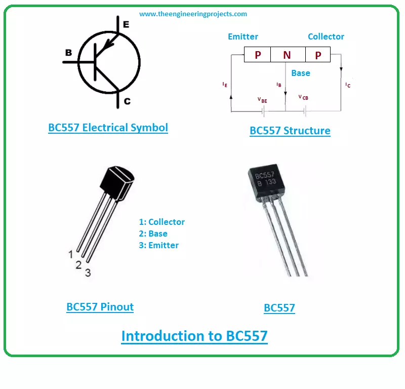
Hi Guys! Hope you’re well. I welcome you on board. Thank you for viewing this read. In this post today, I’ll walk you through the Introduction to BC557.
BC557 is a bipolar junction transistor with DC current gain 300. It falls under the category of PNP transistors where one N-doped layer stands between the two P-doped layers. The continuous collector current is 100mA means it can drive load under 100mA. BC557 comes in the TO-92 package and is mainly used for switching and amplification purpose.
Before I bore you to tears, let’s dive in and read the complete introduction to BC557 covering datasheet, pinout, working principle, power ratings, physical dimensions, and applications.
Continue reading.
Introduction to BC557
BC557 is a bipolar junct ...
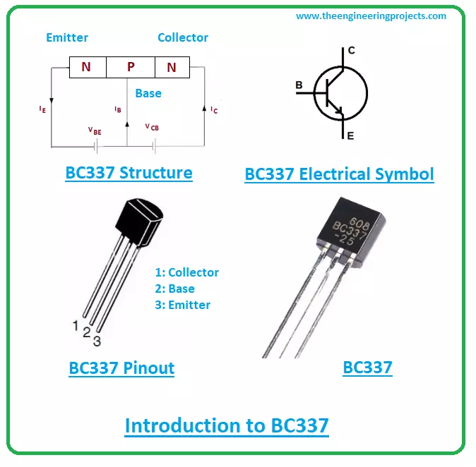
Hi Friends! Hope you’re well today. I welcome you on board. In this post today, I’ll walk you through the Introduction to BC337.
BC337 is a general-purpose transistor mainly used for lower power audio amplification and switching purposes. It belongs to the NPN transistor family and comes with a maximum gain of 630. The continuous collector current is 800mA indicating it can drive loads under 800mA.
I’ll be discussing the complete introduction to BC337 in this post covering pinout, working, power ratings, alternatives, applications, and physical dimensions of BC337.
Stay tuned.
Introduction to BC337
BC337 is an NPN transistor mainly used for lower power audio amplification and switching purposes.
It contains three terminals known as emitt ...
Hi Guys! Glad to see you here. I welcome you on board. In this post today, I’ll be discussing Analog Vibration Sensor Library for Proteus. I have already shared the digital Vibration Sensor Library for Proteus, you should check that as well.
I’ve been adding brand new libraries for proteus covering sensors and Arduino boards. I’ve recently discussed Analog PIR Sensor Library for Proteus and Analog Flex Sensor Library for Proteus. You may be stuck into thinking I’ve previously shared those libraries but they were libraries covering digital PIR and digital Flex sensors, here we discussed analog libraries for both PIR and Flex sensors.
Before I pen down how to download and simulate Analog Vibration Sensor Library for Proteus, let’s discuss what is ...
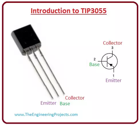
Hello friends, I hope you all are doing great. In today's tutorial, we are gonna have a look at detailed Introduction to TIP3055. TIP3055 is a silicon epitaxial-ignoble NPN transistor, which is assembled in TO-218 malleable parcels. It is the best device for power swapping circuits, parallel and series controllers (regulators), output phases and high power amplifiers. Its corresponding PNP transistor is TIP2955.
It is a universal device used in many industrial projects where audio amplification is required. Its structures are attractive much the identical excluding for the maximum power indulgence that is a slightly lesser. In today’s post, we will have a look at its fortification, smashup, prominence, proposals, etc. I will also share some links ...
Hello friends, I hope you all are doing great. In today’s tutorial, we will have a look at a detailed Introduction to HC-12. It is a wireless data transmitter and receiver module, that uses 433 megahertz frequency and can communicate to one thousand meter distance. It can communicate with more than one microcontroller. This module operates from 3.2 volts to 5.5 volts.
This Bluetooth module is installed in industries to control different processes and machines. It is also used in the circuitry of different security systems. This module uses silicons LABs Si4463 for (radio-frequency) RF data transmission. In today's post, we will look at its working, features, pinout and applications in detail. So let's get started with Introduction to HC-12.
Introduction to HC-12
HC-12 is an RF mo ...
Hello friends, I hope you all are doing great. In today’s tutorial, we will have a look at What is Bistable Multivibrator and how it can be used in different circuits. In this type of multivibrator, the circuitry can operate in any state according to a signal provided at its input while it does not happen in a monostable multivibrator. This arrangement is also defined as a flip flop because flip flop also operates at more than one condition. It also has the ability to store a single bit of information so it is mostly used in logic circuits and in computer data storage part.
This vibrator like other vibrators is used for the production of square waves with providing some delay. These circuits are constructed with numerous kinds of semiconductor components. The most used semiconductor dev ...
Hello fellows, I hope you all are doing great. In today’s tutorial, we will have a look at What is Monostable Multivibrator. It is a simple electronic circuit, used to produce a pulse at its output also known as one shot. It generates output pulses according to corresponding circuitry requirements. Its main feature is that after the generation of the output pulse, it regains its stable state and does not produce any further output pulse till not triggers again.
This circuitry can be considered as a biased form of multivibrator (such circuitry that is used for implementation of 2-state modules like timers) that is (on) operating in the starting condition till the triggered point and then becomes unstable on its own. In today's post, we will have a look at its circuitry, construction, wor ...
Hello friends, I hope you all are doing great. In today's tutorial, we are gonna have a look at detailed Introduction to TIP122. It is a Darlington braces NPN transistor. It works like an ordinary NPN transistor, but as it consists of a Darlington pair it has a decent collector current assessment of nearby 5 amperes and it's gain is around 1000. This transistor can bear 100 volts around collector and emitter terminals due to this feature it can be used for high loads.
This is a common purpose transistor it used in different industrial projects. It manufactured for less time taking switching submissions. In today’s post, we will have a look at its protection, wreck, distinction, entitlements, etc. I will also share some links where I have connecte ...
Hi Guys! Hope you’re well today. Thank you for viewing this read. In this post today, I’ll walk you through the Arduino Mega 1280 Library for Proteus.
You may already be familiar with Arduino Boards, in case you don’t, they are the open-source easy to use hardware and software platform used in modern electronic projects. These boards receive inputs and convert them into outputs to activate motors, LEDs, electrical circuits, robots, and embedded systems.
They are mainly designed for newbies and non-tech geeks who hesitate to construct the electrical circuits from the get-go and hate diving into the nitty-gritty of architecting electrical wires accurately to fashion electrical circuits.
Arduino boards come with both ready-made electronic kit and ...