LM2575 Buck Converter Datasheet, Pinout, Features, Applications

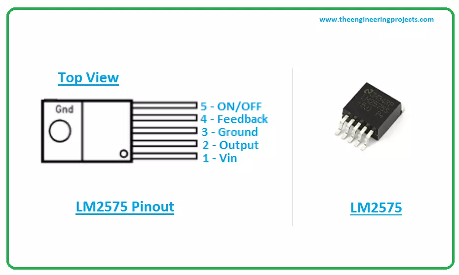
Hi Guys! Glad to see you around. I welcome you on board. In this post today, I’ll walk through the Introduction to LM2575. LM2575 is a step-down voltage regulator mainly used to step down the voltage. It is also known as a buck converter and is used to drive load under 1A. In the customized output version of the buck converter, you can set the output voltage as you like better. It comes with an extremely good load and line regulation and is available in fixed output voltages with 3.3V, 5V, and 12V. I suggest you read this post all the way through, as in this post I’ll detail the Introduction to LM2575 covering the datasheet, pinout, features, and applications of this component LM2575. Let’s get started.

Introduction to LM2575

  • LM2575 is a voltage regulator and simplified version of switching power supplies that carry all functions required to step down the voltage in the circuit.
  • This buck converter is incorporated with an integrated switch that can support load under 1A.
  • LM2575 carries an excellent load line and load regulation. It comes in two versions: fixed output voltage version with voltage 3.3V, 5V, 12V, and adjustable output version that gives the ability to pick your desired output.
  • It is also called the DC-to-DC power converter employed to step down the voltage from its input supply to its output load. The current increases during this voltage regulation.
  • This regulator is integrated with a fixed-frequency oscillator of about 52 kHz and an in-built frequency compensation method.
  • Frequency compensation is applied to reduce vibration and oscillation in the circuit. It can be obtained using resistance-capacitance networks.
  • Apart from the remarkable load and line regulation, this device comes with a manual shutdown option through an external ON/OFF pin.
  • Less external components are needed for this buck converter since it works at a fixed frequency of 52 kHz.

LM2575 Features

  • Fixed versions with 3.3-V, 5-V, 12-V, and adjustable output versions
  • Adjustable output version with voltage range: 1.2-V to 37-V ±4% maximum over load and line conditions
  • Available in two packages named TO-263 and TO-220 packages.
  • Can drive load under 1A.
  • Comes with low power standby mode, commonly less than 200 µA.
  • Uses easily available standard inductors and is highly efficient.
  • 4.75 to 40 V is the input voltage range.
  • 23V to 37V is the output voltage range.
  • 80% efficiency.
  • Excellent load and line regulations.
  • Fixed internal oscillator frequency of 52 kHz.
  • TTL shutdown capability.
  • Protection against overcurrent and thermal shutdown.

LM2575 Pinout

LM2575 comes with five terminals. The following figure shows the pinout diagram of LM2575. ON/OFF = I = this terminal can shut down the voltage regulator circuit with input supply current decreasing to 50uA. Its working is simple and straightforward. When the voltage available on this pin is turned below the threshold voltage of 1.3V, it results in turning on the voltage regulator. And when the voltage is turned above the 1.3V, it results in turning off the voltage converter. You can remove this shutdown feature by connecting the pin to the ground or leaving it open. In both cases, the regulator will be turned ON. VIN = I = this is the 16 number input terminal attached with the input bypass capacitor to reduce voltage transients and to provide the switching current. Output = O = this is the 3 number pin that acts like an internal switch where voltage switches between (Vin – Vsat) and -0.5V. The duty cycle on this pin is Vout/Vin. The PCB copper area connected to this pin is mainly used to reduce the coupling. Ground = three pins number 5,12 & 13 are attached to the ground. Feedback = I = this is the 7 number pin that indicates the regulated output voltage for the feedback loop.

LM2575 Datasheet

Before you install this component into your project, it’s wise to scan through the datasheet that covers the main characteristics of the component. Click the link below and download the datasheet of LM2575.

LM2575 Applications

LM2575 is used in the following applications.
  • Used in a simple efficient step-down regulator.
  • Used as a pre-regulator in linear regulator
  • Used to drive load under 1A.
  • Incorporated in On-card switching regulators.
  • Employed in a positive-to-negative converter.
That was all about the Introduction to LM2575. Hope you find this post helpful. If you have any query, you can approach me in the section below, I’d love to help you the best way I can. Feel free to keep us updated with your valuable feedback and suggestions, they help us produce quality content customized to your exact needs and requirements. Thank you for reading the article.

Introduction to Arduino Esplora

Hi Guys! Hope you’re well today. I welcome you on board. In this post today, I’ll walk you through the Introduction to Arduino Esplora. Looking like a videogame controller, the Arduino Esplora is an electrical device that contains an Arduino Leonardo board (microcontroller) and a number of outputs and inputs. There are a colored LED and a buzzer as outputs. And there is a light sensor, four buttons, a joystick, a microphone, an accelerometer, and a temperature sensor as inputs. In other words, it is just like another Arduino Board with integrated actuators and sensors. Just stay with me for a little while, as I’m going to document the complete Introduction to Arduino Esplora covering pinout, working, pin description, how it’s different than other Arduino boards, and applications. Let’s jump right in.

Introduction to Arduino Esplora

  • Introduced by Arduino.cc, the Arduino Esplora is an electrical device that is based on the Arduino Leonardo board and contains integrated actuators and sensors.
  • Similar to the Arduino Leonardo, the Esplora board is incorporated with an Atmega32U4 AVR microcontroller that carries a 16 MHz crystal oscillator.
  • The Esplora comes with onboard light and sound outputs, and many input sensors, like a temperature sensor, an accelerometer, a joystick, a slider, a light sensor, and a microphone.
  • It also contains two Tinkerkit input and output connectors to enhance its capabilities and a socket used for the LCD screen.
  • Arduino Boards like Arduino Esplora are developed to provide both hardware and software platforms in one place. You can control the board with Arduino software as you like better. Plug and play with the device without getting hands-on experience in electronics.
  • It can mimic a keyboard or mouse that gives you the ability to use it with any 3D software.
  • Arduino Esplora board contains two actuators and 11 inputs. It carries a light sensor, an accelerometer, a multiplexer, and a mic, an RGB LED, and a buzzer.
  • This board contains all built-in sensors and actuators, the reason it’s easy to program and easy to handle through Arduino IDE software.
  • The Arduino Esplora is a great package for beginners, with built-in features, giving you the ability to plug and play with the device and get desired results on the fly.
  • This board is not compatible with the Arduino Shields, but you can connect this device with the external LCD module.
  • To connect the other modules, this device carries two output and two input ports. These ports are compatible with the signal, voltage, and ground pins and are known as 2 pin TinkerKit ports.
  • The Arduino Esplora is an ideal pick for creating a remote control device for your electrical project. You can develop external communication with your project without any hassle.
  • A micro USB cable is attached to the board, and it carries almost everything to get you started without having to combine and assemble anything from outside.
  • Information is extracted from the inputs and is used to write the program in the software which is then used to control the outputs on the board or your computer just like a remote controller.
  • Arduino Esplora is compatible with the Arduino IDE (Integrated Development Environment) like other boards.
  • Plus, you can also run this device with Arduino Web Editor that is hosted online and is incorporated with the latest support and features for all boards. Read this guide on how to use this browser and upload your sketches online.
  • And if you want to use this board offline, you need to install the Arduino IDE desktop version.
  • This board contains everything built-in to get you started. You need to simply connect the board with the computer through USB cable and start your work.
  • The reset pushbutton is located at the upper left corner that is used to restart the board.
Esplora carries four LEDs as follows:
  • ON LED is colored green that identifies if the board is getting a power supply
  • Accessible through pin 13, L is a yellow LED that is directly connected to the microcontroller.
  • RX and TX are yellow LEDs that determines the information received or transmitted through USB communication.

Arduino Esplora Features

The following are the sensors available on the Esplora board:
  • Joystick
  • push-button of the joystick
  • microphone
  • light sensor
  • 2 TinkerKit input connectors
  • temperature sensor
  • 4 separate push-buttons
  • Accelerometer
The following are the actuators present on the board:
  • RGB LED
  • Buzzer
  • 2 TinkerKit connectors

Arduino Esplora Set up with Windows

  • First, you require a standard software developed by Arduino.cc known as Arduino IDE. This software is used to program and control the board through your system.
  • Now connect the board with the computer through micro USB that is used to transfer the program from the computer system to the board.
  • As you connect the cable the green power LED (labeled ON) will turn on and then the yellow LED will start glowing that is marked ‘L’. The yellow LED will go blinking on and off after 8 seconds indicating your board is connected with the computer.
  • When you connect the board, the Windows will automatically start its driver installation process. It the installation process doesn’t start automatically, go to the windows device manager then (Start > Control Panel > Hardware) and go to the Arduino Esplora listing. Right-click this listing and pick Update driver.
  •  At the next popped up window, select "Browse my computer for driver software", and click Next
  • Now click the ‘Browse’ option. It will return another window: find the folder with the Arduino software that you have installed. Choose the drivers folder and click OK, then click the ‘Next’ button
  • You will get a notification that reads, “the board has not passed Windows Logo testing.” Click on the option “Continue Anyway.”
  • After a while, a window will open that reads “Windows has finished installing the driver software for this device” Now click the ‘close’ button.
These instructions are for the system having Windows 7 operating system. If you have a MAC or Linux then read this post on how to connect Arduino Esplora with the system. All pictures placed here are from Arduino.cc

Applications

The following are the applications of Arduino Esplora.
  • Used in Arduino Wifi remote controller
  • Used in robotics and electronics
  • Incorporated to identify free-fall detection using an accelerometer
  • Employed to emulate mouse or keyboard
That’s all for today. I hope you find this read helpful. If you have any questions, you can approach me in the section below, I’d love to help you the best way I can. Feel free to keep us updated with your valuable feedback and suggestions, they help us generate quality work customized to your exact needs and requirements. Thank you for reading the article.

Introduction to TIP42

Hi Guys! Thank you for clicking this read. Hope this finds you well. In this post today, I’ll document the Introduction to Tip42. Tip42 is a medium power silicon transistor mainly used for switching and amplification purpose. It belongs to the PNP transistor family and comes in the TO-220 package. The collector current is 6A which signals it can support load under 6A. Both collector-base and the collector-emitter voltages are 40V. And the only 5V is required to initiate the transistor action as the emitter-base voltage is 5V. The power dissipation is 65W which defines the amount of energy released during the working of this transistor. The storage junction temperature is -65 to 150C and transition frequency is 3MHz. Just stay with me for 2-min as I’ll be discussing the main features, pinout, datasheet, and applications of the device Tip42. Let’s jump right in.

Introduction to TIP42

    • Tip42 is an epitaxial medium power silicon transistor mainly used for switching and amplification purpose. It falls under the category of PNP transistor and comes with current gain ranging from 15 to 75.
    • This current gain demonstrates the capacity of transistor it can amplify the current. It’s a ratio between the output current and input current.
    • Tip42 is a bipolar transistor which means two charge carriers are used in the conductivity process inside the transistor.
    • Both electrons and holes take part in the conductivity process. And in this case of PNP transistor, holes are majority carriers. And electrons are minority carriers in the case of NPN transistors.
  • This PNP transistor contains three terminals called the emitter, base, and collector. All these terminals carry different functionality and different doping concentration.
  • This different doping concentration is the main reason this bipolar transistor is not symmetrical. The external circuit is connected with the transistor through these terminals.
  • Tip42 is composed of two p-doped layers and one n-doped layer. The n-doped layer is sandwiched between the two p-doped layers. The two p-layers represent the collector and emitter terminals and the n-layer represents the base terminal. The N sign shows, a negative voltage is applied on the base terminal to trigger and start the transistor action.
  • This bipolar transistor controls the small input current and produces the large output current, the reason these devices are called current-controlled devices because two charge carriers are used for conductivity in contrast to FETs(field effect transistor) which is unipolar voltage-controlled devices. Where conductivity is carried out with only one charge carrier.
 

TIP42 Features

The following are the main features of transistor BC538.
  • Package: TO-220
  • Material: Silicon
  • Type – PNP
  • Emitter-Base Voltage: 5 V
  • Collector-Base Voltage: 40 V
  • Collector-Emitter Voltage: 40 V
  • Collector Dissipation: 65 W
  • Collector Current: 6 A
  • Transition Frequency: 3 MHz
  • Current Gain (hfe): 15 to 75
  • Storage Junction Temperature: -65 to +150 °C
  These are the main features and absolute maximum ratings of the device Tip42. Make sure you don’t apply these ratings for more than the required time, otherwise it will harm your device reliability.
  • Plus, make sure your ratings don’t exceed these absolute maximum ratings while you’re working with the device, otherwise they will badly damage the device and thus the entire project.
  • Both collector-emitter and collector-base voltages are 40V while the emitter-base voltage is 5V which projects you need to apply 5V to initiate the transistor action.
  • The Collector current is 6V which indicates this transistor can support load under 6A. The transition frequency is 3MHz and power dissipation is 65W which is the amount of energy released during the working of this transistor.
  • DC common-emitter current gain ranges from 15 to 75. It is a ratio between collector current and base current. This describes the capacity of transistors it can amplify the current. This is a relation between output amplified current to input small current.
  • Another important current gain is the common-base current gain which is a ratio between collector current and emitter current and its value is always less than one. Normally ranges from 0.5 to 0.95.
  • The small current at one pair of terminals is used to produce large current across other pairs of terminals of the transistor and this process is used for amplification purposes.
  • It is important to note that the PNP transistors are less likely to employ for amplification purposes than NPN transistors. Because the mobility of electrons in the NPN transistor is far better and quicker than the mobility of holes in PNP transistors.
 

TIP42 Pinout

The Tip42 consists of three main terminals called: 1: Base 2: Collector 3: Emitter The following figure shows the pinout diagram of Tip42.
  • The collector terminal is lightly doped and the emitter terminal is highly doped in contrast to the other two terminals.
  • The collector terminal is 10-times lightly doped than the base terminal. And this transistor is manufactured in such a way, the collector side covers the entire emitter terminal area.
  • The base terminal is responsible for the entire transistor action.
  • This base terminal acts like a control valve that controls the number of holes in the case of the PNP transistor and the number of electrons in the case of NPN transistor.
  • When 5V is applied at the base terminal, it gets biased and starts the transistor action where current moves from emitter to collector terminal which is the opposite in the case of NPN transistors where current moves from collector to emitter terminal. And in both cases base terminal controls the amount of current passing through it.

TIP42 Datasheet

Before you apply this device into your project, scan through the datasheet of the component that helps you get a hold of the main characteristics of the device. You can download the datasheet of Tip42 by clicking the link below.

TIP42 Applications

Tip42 is used in the following applications.
  • Used for switching and amplification purpose.
  • Used to drive load under 6A.
  • Incorporated in the motor control circuit
  • Employed in H-bridge circuit
  • Incorporated in the voltage regulator circuit
That’s all for today. I hope you’ve got a clear insight into the Introduction to Tip42. If you’re unsure or have any question, you can pop your question in the comment section below, I’d love to assist you the best way I can. Keep your suggestions and feedback coming, they help us create quality content customized to your exact needs and requirements. Thank you for reading the article.

Introduction to TIP42C

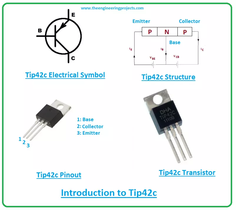
Hi Friends! I welcome you on board. Happy to see you around. In this post, I’ll detail the Introduction to Tip42c. Tip42c is a medium power transistor mainly used for amplification and switching purpose. It is made up of silicon material and falls under the category of PNP transistors. The voltage across collector and emitter terminals is 100V and the voltage across base and collector terminals is 100V. The 5V is the voltage across base and emitter terminals which projects the value of voltage required to bias this transistor. The 6A is collector current which indicates the value of loads this transistor can support. Just bear with me for a little while as I’ll be documenting the main features, pinout, applications, and datasheet of this tiny component Tip42c.

Introduction to TIP42C

  • Tip42c is a PNP medium power bipolar transistor mainly used for switching and amplification purpose.
  • It is composed of silicon material and comes in the TO-220 package.
  • It comes with three pins called the emitter, base, and collector. These pins are also known as transistor terminals that are connected with the external electrical circuit.
  • The small input current across one pair of terminals is used to generate large output current across other pairs of terminals.
  • Tip42c contains three layers where two are p-doped silicon layers and one is an n-doped silicon layer. The n-doped layer represents the base terminal where negative voltage is applied to start the transistor action. The two p-doped layers surround the n-doped layer.
  • As this bipolar transistor controls the small current to produce large current, the reason bipolar transistors are considered as a current-controlled device in contrast to FETs(field effect transistor) which is a unipolar transistor (conductivity happens due to one charge carrier) that are voltage-controlled devices.
  • Two current-gains are important while studying bipolar transistors. One is a common-emitter current gain which ranges from 15 to 75 in this case and common-base current gain which is a ratio between collector current to emitter current, this is normally called alpha.
Its value is always less than 1, commonly lies from 0.90 to 0.95 but more often than not its value is taken as unity.  

TIP42C Features

The following are the main features of device Tip42c
  • Name: TIP42C
  • Package: TO220
  • Material used: Silicon
  • Type: PNP
  • Power Dissipation: 65 W
  • Collector-Base Voltage = Vcb: 100 V
  • Collector-Emitter Voltage = Vce: 100 V
  • Emitter-Base Voltage = Veb: 5 V
  • Collector Current = Ic : 6 A
  • Operating Junction Temperature = Ti:  -65 to 150 °C
  • Transition Frequency = ft: 3 MHz
  • Common-emitter current gain = hfe: 15 to 75
These are the main features and the power ratings of the transistor Tip42c. Don't apply these ratings for more than the desired time, else they will influence the device reliability.
  • The Tip42c is a bipolar transistor which means two charge carriers are used for the conduction process inside the transistor. Both electrons and holes are used for the conductivity, however, holes are the majority carriers and electrons are the minority carriers. Which is the opposite in the case of NPN transistor where electrons are the majority carriers and holes are minority carriers.
  • This PNP transistor comes in TO-220 package with collector current 6A which demonstrates it can support the loads under 6A.
  • The junction temperature ranges from -65 to 150C and the transition frequency is 3MHz which is a measure of the transistor’s high frequency operating characteristics. It is denoted by ft.
  • The common-emitter current gain stands from 15 to 75 which is the capacity of the transistor it can amplify the small input current. It is called beta and is a ratio between output collector current to input base current.
  • And the only 5V is required to start the transistor action because 5V is the voltage across emitter and base terminals.
  • It is important to note that this PNP transistor is not preferred over its counterpart NPN transistor because the mobility of electrons in the NPN transistors is quicker and better than the mobility of holes inside the PNP transistor.
  • Moreover, in NPN transistors the current flows from the collector side to the emitter side in contrast to PNP transistors where current moves from the emitter side to the collector side.
  • The 65W is the power dissipation that indicates the energy released when this transistor starts working in the electrical circuit. This varies from transistor to transistor.

TIP42C Pinout

The Tip42c contains three terminals named: 1: Base 2: Collector 3: Emitter The following diagram shows the pinout of the transistor Tip42c.
  • All these terminals carry different doping concentrations and different working ability. The emitter side is more doped compared to the other two terminals and the collector side is lightly doped. The base side is 10-times more doped than the collector terminals.
  • This bipolar transistor is not symmetrical. This absence of symmetry is due to the different doping concentration of the emitter and collector terminals.
  • In bipolar transistors, the base terminal is responsible for the entire transistor action. When voltage is applied at the base terminal, it gets biased and starts controlling the number of holes in this case of PNP transistors and the number of electrons in the case of NPN transistors.
  • This base terminal acts like a control valve that controls the amount of current. The emitter terminal is highly doped and contains the entire current of the transistor. The emitter current is equal to the sum of the collector current and base current.
 

TIP42C Datasheet

When you’re working with tiny devices like Tip42c, it is wise to scan through the datasheet of the component that documents the main characteristics of the transistor. Click the link below and download the datasheet of Tip42c.

TIP42C Applications

The Tips42c is used in the following applications.
  • Used for switching and amplification applications
  • Used in motor control drivers
  • Employed in H-bridge circuits
  • Incorporated in voltage regulator circuits
  • Used to drive loads under 6A
That’s all for today. I hope you find this article helpful. If you’re unsure or have any question, you can pop your query in the section below, I’d love to help you the best way I can. Feel free to leave your valuable suggestions and feedback, they assist us to generate quality content customized to your exact requirements. Thank you for reading the article.

Introduction to C1815

Hello friends, I hope you all are doing great. In today's tutorial, we are gonna have a look at detailed Introduction to C1815. The C1815 is a transistor like other it is used to amplify acoustic frequency signal. Most transistors are coded for easy documentation through these titles can differ by builders. One or two erudition are typically trailed by a sequence of statistics, and then probably additional statistics. Consequently, a C1815 transistor can also be recognized as a 2SC1815 transistor. It is used as a switch to initiative loads below 150mA. The use of transistors aided the electronics manufacturing alteration quickly, and developments in expertise are permitting minor apparatuses to be used to production of slighter expedients. In today’s post, we will have a look at its shield, wreckages, implication, proposals, etc. I will also share some links where I have connected it with other microcontrollers. You can also get more material about it in comments, I will guide you more about it. So, let’s get started with a basic Introduction to C1815

Introduction to C1815

  • The C1815 is a transistor like other it is used to amplify acoustic frequency signal. It is used as a switch to initiative loads below 150mA.
  • It is manufactured from semiconductors constituents such as Silicon, Germanium, etc, it has three pinouts sometime extra.
  • It is used for swapping and strengthening of numerous signals. Additional statistics can also be found only from the part digits.
  • The '2S' ratio of the integer designates that the C1815 transistor is decent for high-frequency solicitations and is in Negative-Positive-Negative arrangement.

  • The first negative terminal of the transistor is associated with the negative sideways of a circuit, and monitor the movement of electrons to the positive area in the intermediate.

  • The second negative terminal of the transistor governs the electrons sendoff the positive, central area.

  • The semiconductor component that is used to develop the transistor decide that the transistor have NPN or PNP pattern.
  • Three leads on this transistor recognized the emitter, base, and collector. An emitter is a yield, the base is similar to the doorway which switches the input of the collector.
  • For instance, while a C1815 transistor is used in an audiovisual solicitation, the emitter directs the audiovisual output signal. This is managed by the base, which can be a squat audiovisual signal, and motorized by the collector, which might be a 5-volt power source.
  • By fluctuating the quantity of current at the base terminal of a transistor, the extent of power moving from the collector to the emitter can be organized.
  • For illustration, in numerical circuits, a transistor is on condition when it accepts 5-volts, and off when it takes fewer than that quantity.
  • Overall evaluations for a C1815 transistor comprise a power indulgence of 0.4 watts at an ambient temperature of 77° Fahrenheit (25° Celsius). The transistor consumes collector current of 0.15 amps. Quantity of voltage amid collector and base is 60 volts.

Pinout of C1815

  • These are pinout of C1815.
    Pin# Type                                         Parameters
    Pin#1 Emitter This pin is for the outward movement of current.
    Pin#2 Base The base governs the biasing of the transistor.
    Pin#3 Collector The collector is for the current inner drive. It is associated with the load.
    Lest see a diagram of the pinout.

Features of C1815

  • These are some features of C1815.
    • It is offered in cascading of TO-92.
    • It is like an NPN transistor.
    • The quantity of current across collector (Ic) is 150mA.
    • The value of voltage across the collector to the emitter(VCE) is 50V.
    • The quantity of voltage crossways its emitter and base (VEB) is 5V.
    • Voltage crosswise collector and base (VCB) is 60V.
    • Intemperance power crossways collector is 400mW.
    • Its frequency conversion is 80MHZ.
    • It lowermost current gain is 70 and extreme is 700.
    • Its extreme stowage and the employed temperature is -55 to +150 C.

Where we can use C1815

  • As it is C1815 transistor it can be used in acoustic intensifications phases, trivial acoustic amplifier, pre-amplifier and also in pre-amplifier phases.
  • It works as a switch in electronic circuits to run loads of 150mA such as to run relay, high power consuming transistors, LEDs and other industrial electronic circuits.
  • It works as a switch in electronic circuits to run loads of 150mA such as to run relay, high power consuming transistors, LEDs and other industrial electronic circuits.
  • We can use it to construct a Darlington pair.

Applications of C1815 

  • These are applications of C1815.
    • It is used in such instruments which use Sensor Circuits
    • It is used in Auditory Pre-amplifiers.
    • It is used in different audio Amplifier Phases.
    • It works as a switch for such circuits which use 150mA current.
    • It used in RF Circuits.
 So it was all about C1815 if you have any question about it ask in comments. I will explain to you further about it. Thanks for reading.

2SB772 Transistor Pinout, Features, Datasheet & Applications

Hello everyone! I welcome you on board. Hope you’re well. In this post today, I’ll detail the Introduction to 2sb772. 2sb772 is a PNP transistor that comes in the TO-126 package. It is mainly used for amplification and switching purposes. This is a bipolar junction transistor which means the conductivity is carried out by two charge carriers i.e. holes and electrons. And it comprises of two junctions where the base-emitter junction is forward biased and the base-collector junction is reverse biased in forward active mode. In this post, I’ll be discussing the working principle, pinout, datasheet, physical dimensions, power ratings, and applications of the device 2sb772. Let’s get started.

Introduction to 2SB772

  • The 2sb772 is a medium power PNP bipolar junction transistor mainly employed for switching and amplification purpose.
  • It comes with three main terminals called the emitter, collector, and base. All these terminals come with different functionality and different doping concentrations.
  • The emitter side is highly doped in contrast to the other two terminals and the collector is lightly doped. The base terminal is 10-times highly doped compared to the collector terminal.
  • 2sb772 is a semiconductor device made up of silicon material and it consists of three layers. Where one is an n-doped layer that stands between two p-doped layers.
  • The n-layer signals the base terminal and indicates that negative voltage supply is required to bias the base terminal and start the overall transistor action.
  • As this is a bipolar transistor, both electrons and holes play a vital role in the conductivity process.
  • And holes are majority carriers while electrons are minority carriers in this case in contrast to NPN transistors where electrons are major carriers and holes are minority carriers.
  • The bipolar transistors like this 2sb772 are the building blocks of modern electronics.
  • In some cases, however, the vacuum tubes are preferred over bipolar transistors since the mobility of charge carriers is far better in vacuum tubes which is suitable for high-power high-frequency applications like on-air television broadcasting.

2SB772 Datasheet

Before installing this component into your project, have a quick look at the datasheet that helps you get a hold of the main characteristics of the device. Click the link below and download the datasheet of 2sb772.

2SB772 Pinout

The 2sb772 carries three main terminals known as 1: Emitter 2: Collector 3: Base The following figure shows the pinout diagram of the 2sb772 transistor.
  • All these terminals are used for the external connection with the circuit. The emitter side carries the overall transistor current.
  • And in this PNP transistor current flows from the emitter to the collector terminal due to the movement of major charge carriers i.e. holes.
  • While the current flows from the collector to the emitter terminal in the case of NPN transistors due to the mobility of electrons.

2SB772 Working Principle

  • The working principle of this transistor is simple and quite similar to NPN transistors. In both NPN and PNP transistors, the base pin is mainly responsible for the overall transistor action.
  • And when a positive voltage is applied at the base terminal it gets biased and current flows due to the movement of holes.
  • When there is no current available at the base terminal, the transistor is turned ON and in that case, both collector and emitter pins are forward biased.
  • And when there’s current present at the base terminal, the device is turned OFF and both emitter and collector terminals are reverse biased.
  • Unlike other transistors, bipolar transistors are not symmetrical. Different doping concentrations of both emitter and collector sides are responsible for the lack of symmetry inside bipolar junction transistors.
  • Moreover, if we exchange the collector and emitter terminals, the common-emitter gain and common-current values will be less than they are normally observed.
  • The common-emitter current gain is called beta and is also known as the amplification factor. In this case, the amplification factor stretches from 30 to 300. This factor determines the amount of input current this transistor can amplify.

2SB772 Power Ratings

The following table shows the absolute maximum ratings of 2sb772.
Absolute Maximum Ratings BC639
No. Rating Symbol Value Unit
1 Collector-Emitter Voltage Vce 30 V
2 Collector-Base Voltage Vcb 60 V
3 Emitter-Base Voltage Veb 5 V
4 Collector Current Ic 3 A
5 Current Gain hfe 30 to 300
6 Power Dissipation Ptot 12.5 W
7 Storage Temperature Tstg -65 to 150 C
  • The collector-base voltage is 60V while the collector-emitter voltage is 30V. And the emitter-base voltage is 5V which means it requires a total 5V to start the transistor action and bias this device.
  • The power dissipation is 12.5W which determines the amount of energy this device releases during the working of this component. Storage temperature lies from -65 to 150 C and the junction temperature is 150C.
  • While working with this device make sure your ratings don’t exceed these absolute maximum ratings, else you’ll risk the component and thus the entire circuit.
  • Also, if you apply these ratings for more than the required time, they will affect device reliability.

2SB772 Alternatives

The following are the alternative to 2sb772.
  • BD186
  • KSB772
  • BD132
  • BD188
  • MJE232
  • BD190
  • MJE235
  • KSH772
Before you incorporate these alternatives into your circuit, double-check the pinout of the alternatives, as it's quite likely the pinout of the alternatives doesn't exactly match with the pinout of the 2sb772. The complementary NPN transistor to 2sb772 is 2sd882.

2SB772 Applications

This device is used in the following applications.
  • Used for amplification and switching purposes.
  • Incorporated in H-bridge circuits.
  • Employed in relay drivers.
  • Incorporated in the motor control circuit.
  • Used in voltage regulator circuits.
  • Used in Astable and Bistable multivibrators.
  • Used to support loads under 3A.

2SB772 Physical dimensions

The following diagram shows the physical dimensions of transistor 2sb772. These dimensions will help you identify the total space required for the entire project. That’s all for today. Hope you find this article helpful. If you are unsure or have any query you can pop your comment in the section below, I’d love to help you the best way I can. You’re most welcome to share your feedback and suggestions, they help us produce quality content customized to your exact requirements. Thanks for reading this post.

TIP41C Transistor Pinout, Features, Datasheet & Applications

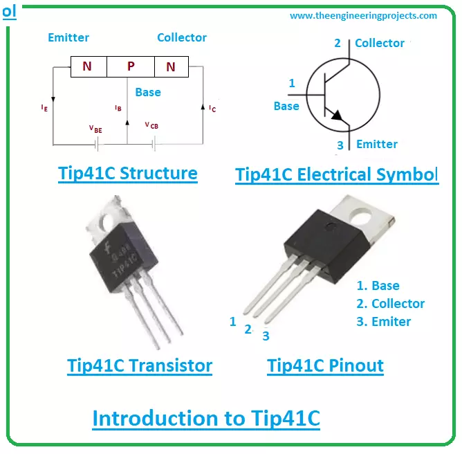
Hi Friends! Welcome you on board. Happy to see you around. In this post today, I’ll walk you through the Introduction to Tip41c. Tip41c is an NPN transistor that comes in the TO-220 package and is mainly used for amplification and switching purposes. It’s a high switching speed device with improved current gain and a high collector current around 6A that indicates the value of load this device can support. Both collector-base and collector-emitter voltages are 100V (higher than other bipolar transistors) and the emitter-base voltage is 5V which shows the only 5V is required to bias this component. Just stay with me for a little while as I’m going to detail the pinout, datasheet, applications, power ratings, working principle, and physical dimensions of this tiny device. Let’s jump right in.

Introduction to TIP41C

  • Tip41C is an electronic tiny device mainly used for switching and amplification purpose. It belongs to the category of NPN transistor and comes with high power around 65W, which is the amount of energy released during the working of this transistor.
  • This NPN transistor comes with three pins, also known as terminals, called the emitter, collector, and base.
  • The small input current across one pair of terminals is used to produce a large current across other pairs of terminals. This process is used for amplification purposes.
  • Tip41c is composed of three layers. One is a p-doped layer and the other two are n-doped layers that are made up of semiconductors (silicon material).
  • The p-doped layer sits between the two n-doped layers. And the p-doped layer is the base terminal and the P sign shows positive voltage is applied at the base terminal to start the transistor action.
  • This device is composed of two junctions. One is the base-emitter junction that is forward biased and the base-collector junction that is reverse biased in forward active mode.
  • The collector current is 6A which is much higher than other bipolar transistors available in the market. This current defines the amount of load this device can support.
  • And common-emitter current gain stretches from 15 to 75 which is the capacity of the transistor it can amplify the input current. It is a ratio between collector current and base current.
  • The transistor frequency is 3MHz which demonstrates how the current gain of the transistor is influenced by the input frequency.
  • This device controls the low input current and produces high output current, the reason this device is called a current-controlled device.
  • This is a bipolar transistor which means two charge carriers are used for the conductivity process i.e. electrons and holes. The electrons are major carriers in NPN transistors and holes are major carriers in PNP transistors.
 

TIP41C Datasheet

Datasheet of any component documents the characteristic and performance of the device through which you understand what the product is about and its power ratings. Click the link below to download the datasheet of Tip41c.

TIP41C Pinout

The Tip41c comes with three terminals named: 1: Base 2: Collector 3: Emitter The following figure shows the pinout diagram of Tip41c.
  • This device is manufactured in such a way, the collector side covers the entire emitter area, making electrons difficult to escape without being collected by the collector terminal.
  • All these pins come with different doping concentrations. The collector side is lightly doped and the emitter side is more doped compared to both base and emitter pin.
  • The collector pin is 10-times lightly doped compared to the base terminal. These pins are used for external connections with the electrical circuit.

TIP41C Working Principle

  • No matter the bipolar transistor you pick, the base pin is responsible for the transistor action in every bipolar transistor. When a positive voltage is applied at the base pin, it gets biased, initiating the transistor action.
  • And the current starts flowing from the collector to the emitter terminal in contrast to the PNP transistor where current flows from emitter to collector terminal.
  • The base pin works like a control valve that controls the number of electrons in this NPN transistor and the number of holes in the PNP transistor.
  • The bipolar transistors are not symmetrical. The lack of symmetry is caused by different doping concentrations of collector and emitter terminals.
  • The two most common current gains are used to demonstrate the nature and current amplification capability… one is a common-emitter gain that 10 to 75 in this case which is a ratio between the collector and base current.
  • It’s is also known as the amplification factor. This factor signals the capacity of transistors it can amplify the small input current. This factor is called beta.
  • Another important factor is a common-base current gain which is a ratio between collector and emitter current. The value of this gain is always less than 1. Most likely stretches from 0.5 to 0.95.

TIP41C Power Ratings

The table below shows the absolute maximum ratings of Tip41c.
Absolute Maximum Ratings of Tip41C
No. Rating Symbol Value Unit
1 Collector-Emitter Voltage Vce 100 V
2 Collector-Base Voltage Vcb 100 V
3 Emitter-Base Voltage Veb 5 V
4 Collector Current Ic 6 A
5 Current Gain hfe 15 to 75
6 Power Dissipation Ptot 65 W
7 Storage Temperature Tstg -65 to 150 C
  • You can see from the table, collector-base and collector-emitter voltages are 100V and the emitter-base voltage is 5V which means it requires 5V to start the transistor action.
  • Total power dissipation is 65W and common-emitter current gain lies from 15 to 75 that defines the capacity of transistor it can amplify the input current. The transition frequency is 3MHz and the storage temperature stands from -65 to 150C.

TIP41C Alternatives

The following are the alternatives to Tip41c.
  • MJE5180
  • 2SD1895
  • MJE5181
  • BC911
  • BD711
Cross-check the pinout of alternatives before you incorporate them into your project. It’s likely the pinout of the alternatives doesn’t exactly match with the Tip41c pinout. To remain on the safe side and to avoid any hassle later, double-check the pinout of the alternatives. The complementary PNP transistor to Tip41c is Tip42c.

TIP41C Applications

This NPN transistor is used in the following applications.
  • Used for amplification and switching purposes.
  • Used to drive load under 6A.
  • Incorporated to drive DC motors.
  • Used in Darlington pairs.
  • Employed for signal amplification and audio amplification.
 

TIP41C Physical dimensions

The following diagram shows the physical dimensions of Tip41c. That’s all for today. I hope you find this article helpful. If you have any question, you can pop your comment in the section below, I’d love to help you the best way I can. You’re most welcome to share your feedback and suggestions, they help us curate content tailored to your exact needs and requirements. Thanks for reading the article.

B772 Transistor Pinout, Features, Datasheet & Applications

Hi Guys! Hope you’re well today. Thank you for clicking this read. In this post today, I’ll walk you through the Introduction to B772. B772 is a medium power bipolar junction transistor mainly used for switching and amplification purpose and belongs to the PNP transistor family. It comes in the TO-126 package and carries a collector current of 3A which means it can support load under 3A. The 60V is the collector-base voltage and 30V is the collector-emitter voltage while 5V is the emitter-base voltage which means it requires 5V to bias the transistor and start transistor action. In this post, I’ll be discussing pinout, datasheet, working principle, power ratings, physical dimensions, and applications of B772. Let’s get started.

Introduction to B772

  • B772 is a bipolar junction transistor that falls under the category of PNP transistors.
  • It contains three pins called the emitter, collector, and base terminals. During the amplification process in the circuit, the small input current present at the base terminal is used to produce large output current at the remaining terminals.
  • This PNP transistor is made up of silicon material and comes in the TO-126 package.
  • B772 comes with three layers where two are p-doped layers and one is n-doped. The n-doped layer stands between two p-doped layers.
  • The two n-doped layers represent collector and emitter and one n-doped layer represents the base terminal and indicates the base terminal requires a negative voltage supply to start the transistor action.
  • You know it already, both electrons and holes play a crucial role in the conductivity process inside the transistor, in the case of PNP transistor holes are majority carriers and electrons are minority carriers in the case of NPN transistors.
  • In comparison, NPN transistors are preferred over PNP transistors because the mobility of electrons is better than the movement of holes in the PNP transistor. In rare cases, both PNP and its complementary NPN transistors are incorporated inside a single circuit.
  • This device is produced using planer technology that generates rugged high-performance components.
 

B772 Datasheet

The datasheet of any component exhibits the main characteristics of the device. It will help you get a hold of the current and voltage required for the emitter, collector, and base terminals. Click below to download the datasheet of B772.

B772 Pinout

B772 carries three main terminals that are known as: 1: Emitter 2: Collector 3: Base The following figure shows the pinout diagram of B772.
  • These terminals are used for the external connection with the electronic circuit. All these pins exhibit different doping concentrations and different functionality.
  • The emitter side is more doped compared to other terminals. Moreover, the emitter terminal contains the entire current of the transistor i.e. Ie = Ic + Ib

B772 Working Principle

  • B772 is a low saturation voltage and high current device where the base terminal is responsible for the overall transistor action.
  • The emitter and collector side is reverse biased when there is current present at the base terminal and in that case, the device is considered turned OFF.
  • And when there is no current at the base side, both collector and emitter are forward biased and the transistor is turned ON.
  • Recall, this is a PNP transistor, here the n-doped layer represents the base side that is negative. The negative voltage supply is applied at the base side to start the transistor working process.

B772 Power Ratings

The following table shows the absolute maximum ratings of the device B772.
Absolute Maximum Ratings B772
No. Rating Symbol Value Unit
1 Collector-Emitter Voltage Vce 30 V
2 Collector-Base Voltage Vcb 60 V
3 Emitter-Base Voltage Veb 5 V
4 Collector Current Ic 3 A
5 Current Gain hfe 30 to 300
6 Power Dissipation Ptot 12.5 W
7 Storage Temperature Tstg -65 to 150 C
  • You can see from the table, the 60V is the collector-base voltage and 30V is the voltage between collector and emitter. While the voltage between emitter and base is 5V.
  • Total power dissipation is 12.5W which signals the amount of energy released during the working of this transistor.
  • Junction temperature is 150C and storage temperature stands between 65 to 150C
  • These are called stress ratings. When you incorporate this device into your project, make sure ratings don’t surpass the absolute maximum ratings.
  • If they exceed the required ratings, it will damage the device and thus the entire project.
 

Difference between PNP and NPN transistors

  • Both NPN and PNP are bipolar junction transistors and work similarly with a few exceptions. The current directions and voltage polarities are reversed.
  • In the case of PNP transistor, the conductivity is carried out from the emitter to the collector side while in the case of NPN transistor the conductivity process is carried out from the collector to the emitter side.
  • Moreover, the holes are majority carriers in the case of PNP transistors and minority carriers in the case of NPN transistors. While electrons are majority carriers in NPN transistors and minority carriers in the case of PNP transistors.
  • And negative voltage is applied at the base pin in the PNP transistor and a positive voltage is applied at the base terminal in the case of NPN transistor.

B772 Alternatives

The following are the alternative to B772.
  • BD186
  • BD132
  • KSB772
  • BD188
  • BD190
  • MJE232
  • KSH772
  • MJE235
While working with the alternatives, cross-check the pinout of the alternatives, as it likely the pinout of the B772 might differ from the pinout of the alternatives. The complementary NPN transistor to D772 is D882.

B772 Applications

  • Used for medium-power switching and amplification applications.
  • Used in the motor control circuit.
  • Incorporated in relay drivers.
  • Incorporated in voltage regulator circuits.
  • Used to drive loads under 3A.
  • Employed in Astable and Bistable multivibrators.
  • Employed in H-bridge circuits.
   

B772 Physical dimensions

The following figure exhibits the physical dimensions of the component that help you identify and evaluate the total space required for the circuit. That’s all for today. Hope you find this article useful. If you have any query, you can pop your question in the section below, I’d love to help you the best way I can. Feel free to share your valuable suggestions and feedback in the comment section, they help us to customize our content based on your exact needs and requirements. Thanks for reading the article.

Introduction to 2SD882

Hi Fellas! Hope you’re doing well today. I welcome you on board. In this post today, I’ll detail the Introduction to 2SD882. 2sd882 is an NPN bipolar junction transistor used for amplification and switching purposes. It is a semiconductor device composed of silicon material and comes in the TO-126 package. As this is a bipolar transistor, here conductivity is carried out by two charge carriers i.e. electrons and holes where electrons are major charge carriers and holes are minority carriers. During the amplification application, the small input current across one pair of terminals is used to produce a large output current across other pairs of terminals. In this post, I’ll walk you through the working principle, pinout, power ratings, alternatives, applications, datasheet, and physical dimensions of the 2sd882 transistor.

Introduction to 2SD882

  • 2sd882 is a medium power transistor that belongs to the NPN transistor family. It contains two junctions… the base-emitter junction which is forward biased and the base-collector junction is reverse biased in forward active mode.
  • This NPN transistor is composed of three layers where one is a p-doped layer that sits between two n-doped layers.
  • 2sd882 carries three terminals called the emitter, collector, and base. The electrical circuit is connected with the transistor through these terminals.
  • It is a high current and low saturation voltage device with common-emitter current gain ranging from 30 to 300. The current gain demonstrates the value of current this transistor can amplify. And this current gain varies depending on the voltage and current characteristics of the transistors.
  • The collector-base voltage is 60V and the collector-emitter voltage is 30V. While the emitter-base voltage is 5V that indicates the amount of voltage it requires to bias the transistor and start the transistor action.
  • In bipolar junction transistors, two charge carriers are used i.e. holes and electrons. And in this NPN transistor current flows from the collector to the emitter side with electrons as major charge carriers and holes as minority carriers.
  • This NPN transistor is manufactured in such a way where the collector side surrounds the emitter side. In this construction, the electrons cannot escape the collector region emitted by the emitter terminal.
 

2SD882 Datasheet

The datasheet of any electronic device demonstrates the main characteristics of the component. This way you can get a hold of the current, voltage, and power ratings of the device. Click the link below to download the datasheet of 2sd882.

2SD882 Pinout

The 2sd882 comes with three pins known as: 1: Emitter 2: Collector 3: Base The following figure represents the pinout diagram of transistor 2sd882.
  • All these terminals come with different doping concentrations. The collector pin is lightly doped and the emitter pin is highly doped compared to other terminals.
  • The collector pin is 10-times less doped compared to the base pin. Moreover, the emitter side contains the entire current of the device.

2SD882 Working Principle

  • When a positive voltage is applied at the base pin, it gets biased and the current flows from the collector to the emitter terminal.
  • Recall, both electrons and holes play a key role in the conductivity process inside a transistor but holes are minority carriers and electrons are majority carriers.
  • It is observed bipolar devices like this transistor are not symmetrical components. This means exchanging the emitter and collector terminals will prevent the transistor from working in forward active mode and put both terminals in the reverse active mode.
  • This can affect and reduce the values of common-emitter current gain and common-base current gain.
  • The lack of symmetry is caused by the different doping concentrations of both emitter and collector terminals.
  • Common-emitter current gain is 30-300 in this transistor, which is denoted by beta and common-base current gain is always less than one which is denoted by alpha.
  • And switching the emitter and collector terminals will put the alpha value somewhere around 0.5 and the beta value less than 300.
  • Also, NPN transistors are preferred over PNP transistors since the mobility of electrons is far better and quicker than the movement of holes.

2SD882 Power Ratings

The following table demonstrates the absolute maximum ratings of 2sd882.
Absolute Maximum Ratings 2sd882
No. Rating Symbol Value Unit
1 Collector-Emitter Voltage Vce 30 V
2 Collector-Base Voltage Vcb 60 V
3 Emitter-Base Voltage Veb 5 V
4 Collector Current Ic 3 A
5 Current Gain hfe 30 to 300
6 Power Dissipation Ptot 12.5 W
7 Storage Temperature Tstg -65 to 150 C
  • The collector-emitter and collector-base voltages are 30 & 60 respectively.
  • And total power dissipation is 12.5W which projects the amount of power released during the working of this device.
  • The junction temperature is 150C and the storage temperature stretches from -65 to 150C.
  • While working with the component, make sure the ratings don’t exceed the absolute maximum ratings. Otherwise, they can damage the device, putting the entire project at risk.
  • Plus, don’t apply these ratings more than the required time, else they can affect device reliability.

2SD882 Alternatives

The following are the alternatives to 2sd882.
  • BD187
  • MJE802
  • BD185
  • BD189
  • BD349
  • MJE182
  • 2SC4342
  • 2SD1693
  • 2SD1712
  • TIP122L
  • BD131
  • 2SD1018
Before installing this device into your electrical circuit, cross-check the pinout of alternatives with the original 2sd882. It is likely the pinout of the 2sd882 might differ from the pinout of the alternatives. Be on the safe side and do your due diligence beforehand. The complementary PNP transistor to 2sd882 is 2sb772

2SD882 Applications

2sd882 is used in the following applications.
  • Used for switching and amplification purpose.
  • Employed to support loads under 3A.
  • Installed in the motor control circuit.
  • Employed in the switched-mode power supply.
  • Used in voltage regulator circuits.
  • Used in H-bridge circuits.
  • Incorporated in modern electronic circuits.
  • Used in Bistable and Astable multivibrators circuit.

2SD882 Physical dimensions

The following figure shows the physical dimensions of the 2sd882 device. By scanning the physical dimensions of this component you can audit the space required for your circuit and install the device appropriately. This is it. If you have any query, you can pop your question in the comment section below, I’d love to help you according to the best of my expertise. You are most welcome to share your valuable feedback and suggestions in the section below and help us create quality content tailored to your exact requirements. Thanks for reading the article.

Introduction to D882

Hi there! Hope this finds you well. I welcome you on board. Thanks for clicking this read. In this post today, I’ll be discussing the Introduction to D882 transistor.

D882 is a general-purpose transistor mainly famous for its high performance. It falls under the category of NPN transistor and is an ideal pick for commercial, educational, and hobbyists’ electronic projects. It comes in TO-126 with collector current 3A, projecting it can drive loads under 3A. There are three pins incorporated on the transistor which are used for external connections. The collector-emitter and collector-base voltages are 30V and 40V respectively with emitter-base voltage 5V, indicating only 5V are required to bias the component.

Read this post all the way through as I’ll walk you through pinout, datasheet, alternatives, working principle, power ratings, applications, and physical dimensions of this tiny electronic component D882.

Let’s jump right in.

Introduction to D882

  • D882 is a general-purpose transistor that belongs to the NPN transistor family. It comes with collector current 5A and is mainly used for switching and amplification purpose.
  • The amplification factor is 60-400. This factor indicates the amount of current this device can amplify.
  • This NPN transistor contains three pins called the emitter, collector, and base. The small current at the base terminal is amplified and produced across the remaining two terminals. This process is used for amplification purposes.
  • D882 consists of three layers where two are n-doped layers and one is a p-doped layer. This p-doped layer represents the base terminal which means a positive voltage supply is applied at the base terminal in contrast to the PNP transistor where the base terminal is negative indicating negative voltage supply is applied at the base terminal.
  • As this is an NPN transistor, here current flows from collector to emitter in opposite to PNP transistors where current flows from emitter to collector terminal.
  • This device controls the input current, the reason it’s known as a current-controlled device and is different than FETs (field effect transistor) that are voltage-controlled devices.
  • Though both holes and electrons play a vital role in the conductivity of the transistor, here in this NPN transistor electrons are majority carriers and holes are minority carriers, indicating major part of the conductivity inside the transistor is done by the movement of electrons which is far better than the movement of holes.
  • This NPN transistor is preferred over PNP transistors for the amplification purpose because electrons prove handy for conductivity compared to holes as they are fast carriers.

D882 Datasheet

The datasheet of any component gives you the characteristics of the device through which you can understand the main features of the component before employing it in your project. Click the link below and download the datasheet of D882.

D882 Pinout

D882 comes with three pins named as:

  1. Emitter
  2. Collector
  3. Base

The following picture shows the pinout diagram of D882.

These pins are also called terminals. The small input current at the base terminal is used to produce a large current at the emitter and collector terminals.

D882 Working Principle

  • The overall transistor action starts from the base pin. The base terminal behaves like a control valve that controls the number of electrons emitted from the emitter terminal which are then collected by the collector terminal that is coupled with a resistor to control the electrical current.
  • Recall, in the NPN transistor the positive voltage supply is applied at the base terminal.
  • The P-doped layer in the NPN transistor represents the base terminal and the other two n-doped layers represent emitter and collector terminals which are negative.
  • Also, this base terminal controls the number of holes in the PNP transistors, as holes are the majority carriers in PNP transistors.
  • When 5V is applied at the base terminal it gets biased and starts the transistor action. The small input current is used to create a large output current at the other two terminals.

D882 Power Ratings

The following table represents the absolute maximum ratings of the D882 transistor:
Absolute Maximum Ratings D882
No. Rating Symbol Value Unit
1 Collector-Emitter Voltage Vce 30 V
2 Collector-Base Voltage Vcb 40 V
3 Emitter-Base Voltage Veb 5 V
4 Collector Current Ic 3 A
5 Current Gain hfe 60 to 400
6 Power Dissipation Ptot 10 W
7 Storage Temperature Tstg -55 to 150 C
  • This device exhibits a collector current of 3A which is ideal for driving LED, bulbs, motors, and relays. The maximum power dissipation is 10W which makes it a valuable pick for the output stages of audio amplifiers.
  • It is important to note that these are the stress ratings which if exceeding the absolute maximum ratings, can badly affect the device and thus the entire project. Keep ratings during the working of this component below absolute maximum ratings.
  • One more thing… don’t apply these ratings for maximum time. If you apply these ratings more than the required time, can affect device reliability.

D882 Alternatives

The following are the alternatives to D882.

  • MJE802
  • BD349
  • BD185
  • BD189
  • MJE182
  • BD187
  • TIP122L
  • 2SC4342
  • 2SD1712
  • BD131
  • 2SD1693
  • 2SD1018

The PNP complementary to 2SD882 is 2SB772. It’s important to remember, before installing alternatives in your project, double-check the pinout of the alternatives which might differ from the pinout of the D882. This will save you from the hassle that might happen later.

D882 Applications

The D882 is mainly used in the following applications.

  • Used for amplification and switching purposes.
  • Used to drive loads under 3A.
  • Installed in H-bridge circuits.
  • Incorporated in voltage regulators and power supply circuits.
  • Used to drive motors and battery charger circuits.

D882 Physical dimensions

The following figure represents the physical dimensions of the D882. These dimensions help you evaluate the total space required for the entire electrical project.

That’s all for today. I hope you find this article helpful. You’re most welcome to share your feedback and suggestions in the comment section, they help us produce quality content customized to your exact needs and requirements. If you have any questions, you can pop your comment in the section below, I’d love to help you the best way I can. Thanks for reading the article.

Syed Zain Nasir

I am Syed Zain Nasir, the founder of <a href=https://www.TheEngineeringProjects.com/>The Engineering Projects</a> (TEP). I am a programmer since 2009 before that I just search things, make small projects and now I am sharing my knowledge through this platform.I also work as a freelancer and did many projects related to programming and electrical circuitry. <a href=https://plus.google.com/+SyedZainNasir/>My Google Profile+</a>

Share
Published by
Syed Zain Nasir