Hi Guys! Hope you’re well today. I welcome you on board. Happy to see you around. In this post today, I’ll detail the Introduction to TL081.TL081 is a high-speed general-purpose JFET input single operational amplifier that comes with high noise immunity and better offset characteristics. It carries high input impedance and low offset current. The offset voltage of this device makes it an ideal match for amplifier applications. It incorporates well-matched bipolar transistors and high-voltage JFET in a compact IC.
Read this post till the end as I’ll detail the complete Introduction to TL081 covering datasheet, pinout, features, and applications. Let’s jump right in.
Introduction to TL081
TL081 is a high-speed JFET input single operational amplifier that comes with high slew rates, ...
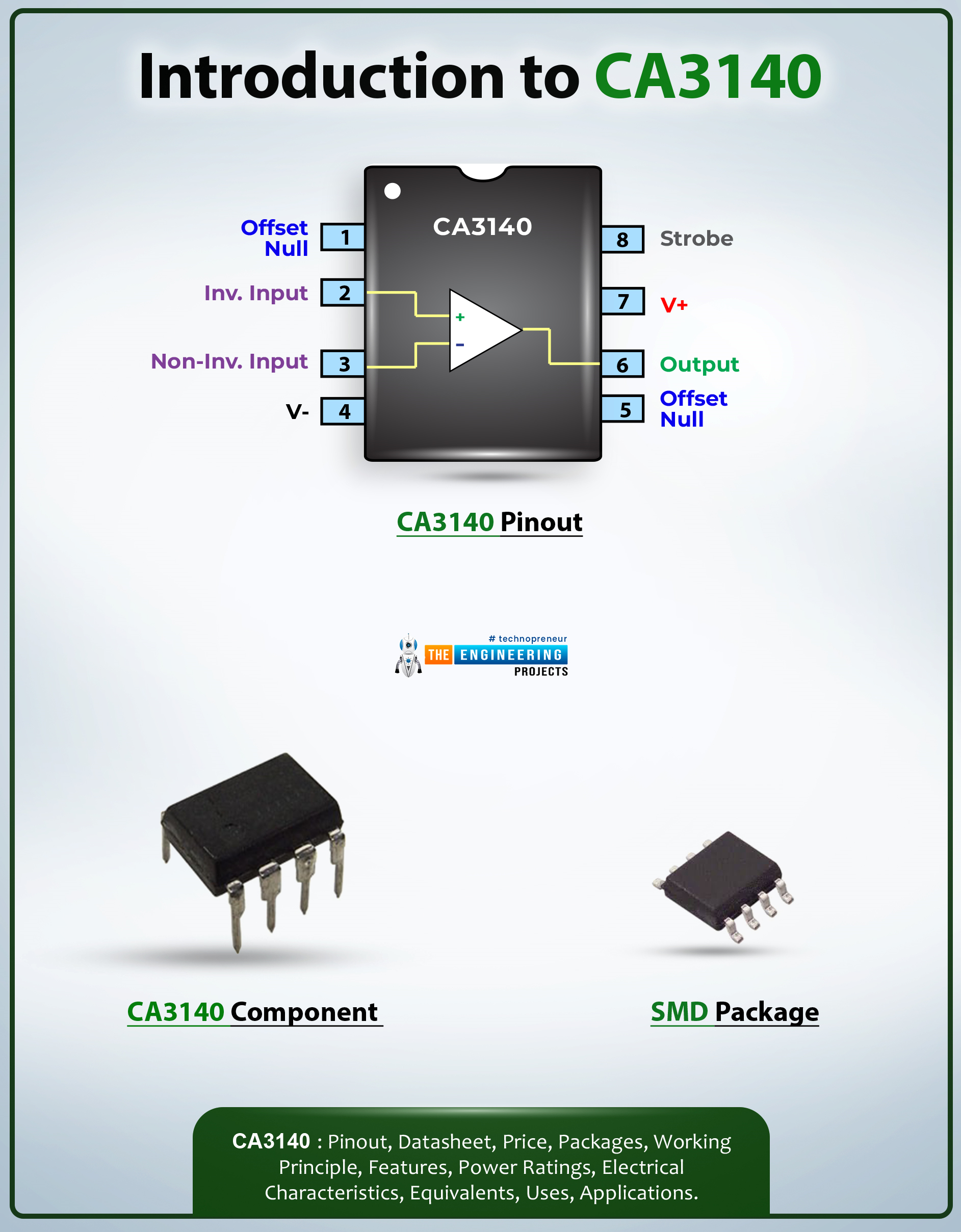
Hi Folks! I welcome you on board. Thank you for clicking this read. Happy to see you around. In this post today, I’ll walk you through the Introduction to CA3140.The CA3140 is a general-purpose op-amp that comes with a 4.5MHz frequency. It is a BiMOS Operational Amplifier incorporated with MOSFET Input/Bipolar Output that extends the advantages of both… high-voltage bipolar transistors and high-voltage PMOS transistors on a single integrated chip.
I suggest you read this post all the way through as I’ll detail the complete Introduction to CA3140 covering datasheet, pinout, features, and applications. Let’s jump right in.
Introduction to CA3140
The CA3140 is a general-purpose op-amp that comes with MOSFET Input/Bipolar Output and extends the advantages of both… high- ...
Hey Guys! Hope you’re well today. Happy to see you around. In this post today, I’ll detail the Introduction to 1n4734a.The 1n4734a is a Zener diode used as a low-current voltage regulator. It is composed of silicon material and is employed as a shunt regulator in many applications. This Zener diode conducts the current in both directions in contrast to a normal diode that conducts in one direction only i.e. conducts in forward biased condition only.
I suggest you read this post all the way through, as I’ll be discussing the datasheet, pinout, features, and applications of 1n4734a. Let’s jump right in.
Introduction to 1n4734A
The 1n4734a is a Zener diode used in clipping circuits with a high power rating.
It comes in the DO-41 package and is used as a low-current voltage regulat ...
Hello Friends! Happy to see you around. I welcome you on board. In this post today, I’ll walk you through the Introduction to 1n4742.The 1n4742 is a Zener diode used for clipping circuits with a high power rating. It is made up of silicon material and comes in the DO-41 package. The Zener diode conducts in both directions i.e. forward-biased condition and reverse-biased condition.
Read this post till the end as I’ll be discussing the datasheet, pinout, features, and applications of 1n4742. Let’s get started.
Introduction to 1N4742
The 1n4742 is a Zener diode that comes in the DO-41 package. It is made up of semiconductor material and is mainly used for clipping circuits with high power ratings.
There is a difference between a diode and a Zener diode. The simple diode conducts i ...
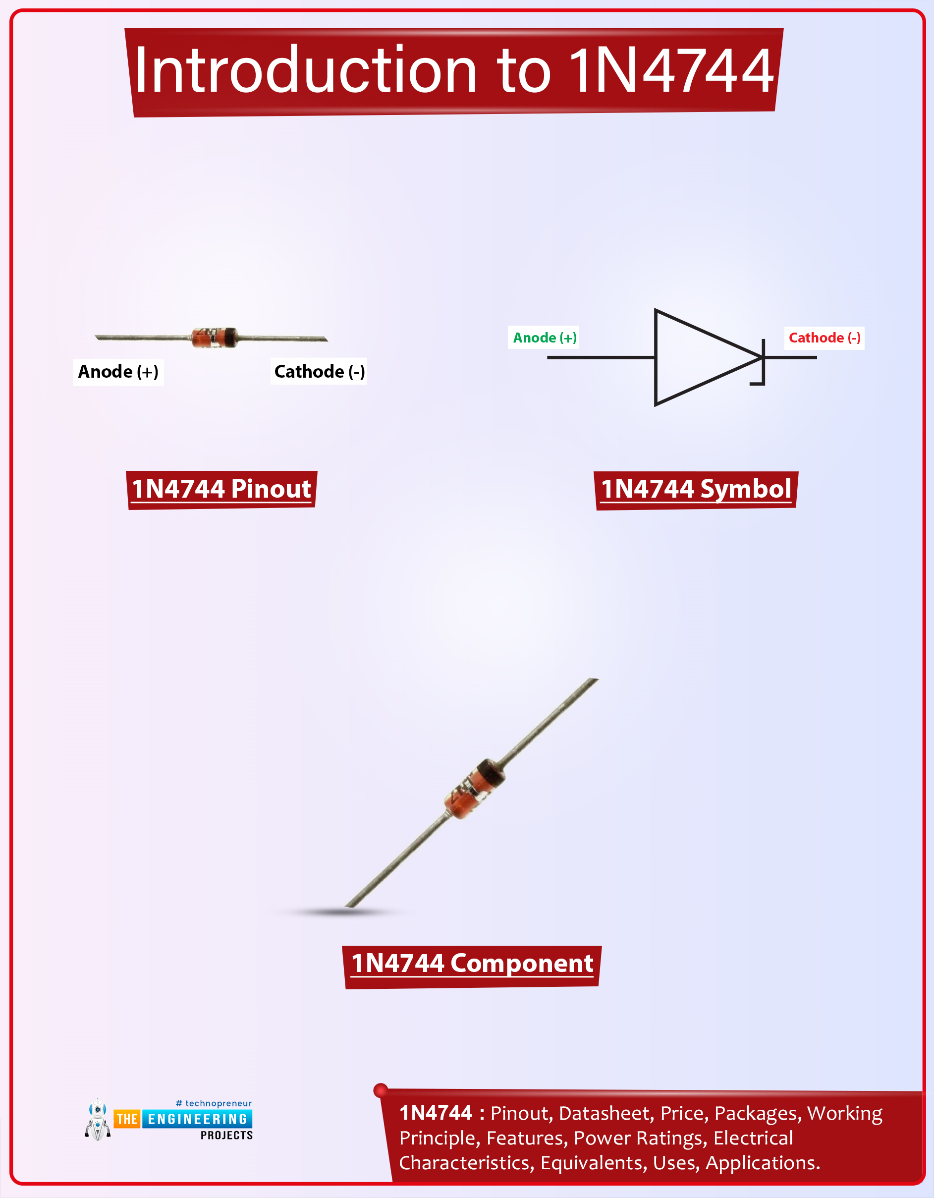
Hello Guys! I welcome you on board. In this post today, I’ll document the detailed Introduction to 1n4744.
The 1n4744 is a Zener diode that comes with a total power dissipation of 1W. It is used in high-power rating circuits for clipping purposes. This component is composed of silicon material and comes with a forward voltage drop of 1.2V. This Zener diode is a bit different than a regular diode in terms of current conduction. The 1n4744 conducts in both directions i.e. forward-biased and reverse-biased conditions. While the regular diode conducts in forward-biased condition only. Zener diodes are also employed to prevent the electrical circuits from overvoltage.
Read the entire post as I’ll detail the datasheet, pinout, features, and applications of 1n4744. Keep reading.
Introduc ...
Hi Guys! Hope you’re well today. I welcome you on board. Happy to see you around. In this post today, I’ll detail the Introduction to Arduino Sensor Shield.
Arduino Sensor Shield is a board compatible with the Arduino Boards and comes with the standard header layout. It is used to connect sensors, servos, LCD with the Arduino board without soldering. This board is connected with the Arduino Board using the jumper wires.
I suggest you read this post all the way through as I’ll be discussing the complete Introduction to Arduino Sensor Shield.
Let’s get started.
Introduction to Arduino Sensor Shield
Arduino Sensor Shield is a board used to connect sensors, servos, LCD with the Arduino Board without the requirement of soldering.
Using Arduino ...
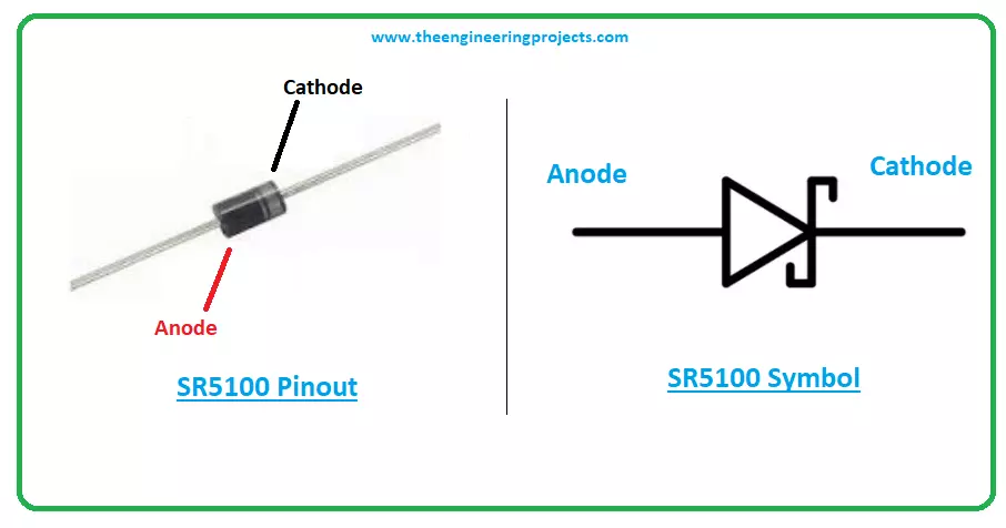
Hi Friends! Hope you’re well today. I welcome you on board. Happy to see you around. In this post today, I’ll walk you through the Introduction to SR5100.
The SR5100 is a Schottky diode used to generate extremely fast switching. It is also called a hot-carrier diode and is protected against overvoltage. It comes with a high surge current capability and low forward drop voltage. It contains a forward rectified current around 5 A and terminal resistance around 28 C/W. It is available in epitaxial construction with a peak reverse voltage of around 100 V.
You are most welcome to see the Introduction to 1n4744 and Introduction to 1n4742 that I have uploaded recently.
Read this post all the way through as I’ll detail the datasheet, pinout, features, ...
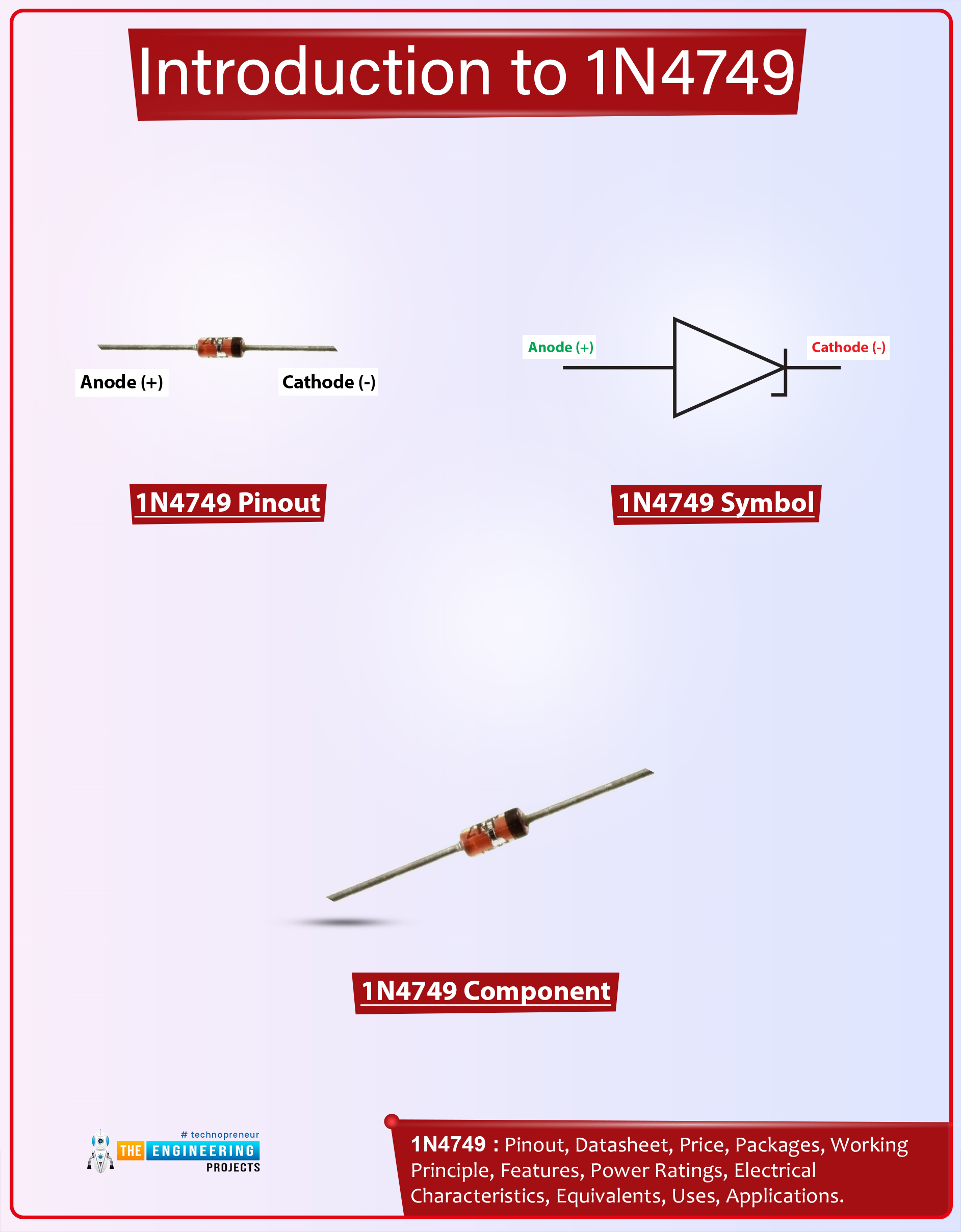
Hello Friends! Happy to see you around. I welcome you on board. In this post today, I’ll walk you through the Introduction to 1n4749.
The 1n4749 is a Zener diode made of silicon material. It is used for clipping circuits with high power ratings. It is also incorporated in voltage stabilizing circuits and voltage protection circuits. There is a slight difference between the normal diode and the Zener diode. In the normal diode, conduction is carried out in one direction only i.e. in forward biased condition. While in the case of the Zener diode, the conduction is carried out in both conditions i.e. forward biased condition and reverse biased condition. Zener diodes are also applied to keep circuits from overvoltage.
Read this post till the end as I’ll walk you through the complete Int ...
Hi Folks! Hope you’re well today. Happy to see you around. In this post today, I’ll detail the Introduction to SB5100.
The SB5100 is a Schottky diode used in electrical circuits to avoid overvoltage. It is also known as a hot-carrier diode and comes with low forward drop voltage. It is capable of high surge current and is used in power management and automotive applications.
You can go through the Introduction to 1n5822 and Introduction to 1n5821 that I have uploaded recently.
Read this entire post till the end as I’ll walk you through the datasheet, pinout, features, and applications of this tiny component SB5100.
Introduction to SB5100
The SB5100 is a Schottky diode, also known as a hot-carrier diode, mainly employed for extremely fast swi ...
Hi everyone! Hope you’re well today. I welcome you on board. In this post today, I’ll walk you through the Introduction to P6KE220A.The P6KE200A is a transient voltage suppressor (TVS) diode that uses clamping action to provide circuit protection against overvoltage. It is widely used in low-voltage supplied ICs and MOS technology due to its quick response to transient overvoltages. For P6KE200A the clamping voltage is 246V and the breakdown voltage is ranged from 190V to 210V.
I suggest you read this entire post till the end as I’ll detail the complete introduction to P6KE200A covering datasheet, pinout, features equivalents, and applications of this component P6KE200A.
Introduction to P6KE200A
The P6KE200A is a transient voltage suppre ...