CA3162 A/D Converter Datasheet, Pinout, Features & Applications

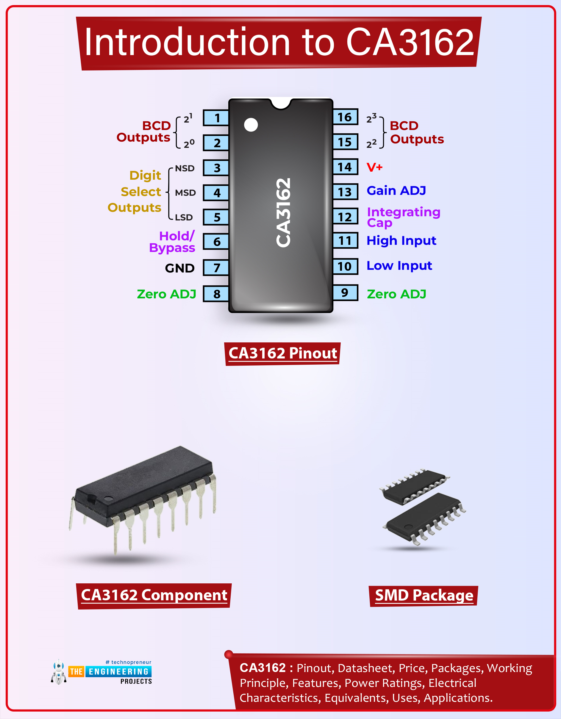
Hi Friends! I welcome you on board. Happy to see you around. In this post today, I’ll detail the Introduction to CA3162.

The CA3162 is a monolithic A/D converter, offering a 3-digit multiplexed BCD output. It comes with an ultra-stable internal band-gap voltage reference. With differential input, this device provides a choice of low-speed (4Hz) or high-speed (96Hz) conversion rate. It is a 16-pin device that provides dual slope A/D conversion.

I suggest you buckle up as I’ll walk you through the complete Introduction to CA3162 covering datasheet, pinout, features, and applications. Without further ado, let’s get started.

Introduction to CA3162

  • The CA3162 is a monolithic A/D converter that offers a 3-digit multiplexed BCD output. It is available with ultra-stable internal bandgap voltage reference.
  • To apply a complete 3-digit display, it is employed with the CA3161E BCD-to-Seven-Segment Decoder/Driver along with a minimum of external parts.
  • A/D converter is a device that converts analog input signals to digital output signals.
  • The environmental quantities are considered analog signals including temperature, sound, time, pressure, etc. are analog quantities.
  • Analog quantities provide value at every instant of time, making it almost impossible to monitor them with digital devices.
  • The reason we often have to convert analog signals to digital signals is so we can analyze this information using digital instruments like CA3162.

CA3162 Datasheet

While working with any component, it’s wise to read the datasheet of the component that details the main characteristics of the device. You can download the datasheet of this component CA3162 by clicking the link mentioned below.

CA3162 Pinout

The CA3162 is a 16-pin device. The pinout diagram of this device is shown below.

  • Pin 1 & 2 are BCD outputs. Pin 3,4,5 are digit select outputs. The input at pin 6 is used to determine the sampling rate. Pin 7 is ground while Pin 8 & 9 are zero adjustment pins which are used to display the zero setting of this device.
  • These pins are considered the starting point of any instrument.
  • Pin 10 & 11 are low input and high input respectively which means the input voltage applied on pins 10 and 11 is converted to a current which in return charges the integrating capacitor incorporated on pin 12 for a predetermined time interval.
  • Pin 14 is a voltage supply pin and pin 15 & 16 are again BCD outputs.

CA3162 Features

The following are the main features of CA3162 that help you understand how this device differs from its peers available in the market.

  • Dual Slope A/D Conversion
  • Multiplexed BCD Display
  • Ultra Stable Internal Band Gap Voltage Reference
  • Capable of Reading 99mV Below Ground with a Single Supply
  • Differential Input
  • Internal Timing - No External Clock Required
  • Choice of Low Speed (4Hz) or High Speed (96Hz) Conversion Rate
  • “Hold” Inhibits Conversion but Maintains Delay
  • Internal Timing
  • Overrange Indication
  • “EEE” for Reading Greater than +999mV

CA3162 Applications

CA3162E can be employed in a 7-segment display or LCD.

That’s all for today. Hope you’ve enjoyed reading this post. If you’re unsure or have any questions in your mind, you can approach me in the section below, I’ll help you the best way I can. Feel free to share your valuable suggestions and feedback around the content we share, and help us create quality content customized to your exact needs and requirements. Thank you for reading the post.

IRF830 MOSFET Datasheet, Pinout, Features, Equivalent & Applications

Hello Guys! Hope you’re well today. I welcome you on board. In this post today, I’ll walk you through the Introduction to IRF830.

The IRF830 is an n-channel power MOSFET where conduction is carried out by both electrons and holes but electrons are the major carriers and holes are the minority carriers. It is a high voltage and fast switching device that comes with low on-state resistance. You can also check this post on the Introduction to IRF730 that I’ve uploaded previously.

I suggest you buckle up and read this post all the way through as I’ll detail the complete Introduction to IRF830 covering datasheet, pinout, features, equivalent, and applications. Let’s get started:

Introduction to IRF830

  • The IRF830 is an n-channel power MOSFET where electrons are the major carriers and holes are the minority carriers.
  • It is widely used in amplification and switching applications of electrical circuits.
  • The MOSFET stands for Metal Oxide Silicon Field Effect Transistor which is produced by the controlled oxidation of a silicon semiconductor material. It is also known as the IGFET Insulated Gate Field Effect Transistor.
  • This device is an n-channel MOSFET which means the conduction is carried out due to the movement of electrons in opposed to the p-channel MOSFET where the conduction process is carried out by the movement of holes.
  • Know that, the conduction process is done by both the movement of electrons and holes but in the case of n-channel MOSFET the major carriers are electrons and in the case of p-channel MOSFET major carriers are holes.
  • With a maximum drain-to-source voltage of around 500V, this IRF830 MOSFET is a three-pin component made of gate (G) drain (D), and source (S) terminals. These terminals are used for the external connection with the electrical circuits.
  • In terms of the controlled value, the MOSFET is different from the BJT semiconductors. The MOSFETs are voltage-controlled devices while the BJT (bipolar junction transistors) are current-controlled devices.
  • These devices, however, are the same in terms of performance and efficiency. Both are high-speed and low-power loss devices.
  • The voltage at the gate pin controls the current between the source and drain terminals. The gate terminal behaves like a control valve that controls the conduction between source and drain terminals.
  • When a voltage signal is applied at the gate terminal, the current starts flowing between the source and drain terminals.

IRF830 Datasheet

Before applying this component to your electrical project, it’s better to go through the datasheet of the component that highlights the main characteristics of the device. You can download the datasheet of this component IRF830 by clicking the link mentioned below.

IRF830 Pinout

The IRF830 is an N-channel power MOSFET that contains three pins named:

  1. Gate
  2. Drain
  3. Source
  • The gate pin controls the current between the source and drain terminals when we apply a voltage signal on the gate pin
  • The following figure shows the pinout diagram of IRF830 MOSFET.

Know that… typically, the MOSFET is a four-pin device that comes with a Source (S), Gate (G), Drain (D), and a Body (B) / Substrate. The bodyside is always connected to the source terminal thus the MOSFET operates as a three-terminal device.

IRF830 Equivalent

The following are the equivalent of IRF830.

  • FTK480
  • 8N50
  • KF12N50

While working with the alternatives, always check the pinout as the pinout of the alternatives might differ from the pinout of this device.

IRF830 Features

The following are the main features of IRF830. These features will help you understand how this device is different from its peers available in the market.

  • Type = n-channel power MOSFET
  • Package = TO-220
  • Gate threshold voltage (VGS-th) = 10V (limit = ±20V)
  • Continuous Drain Current (ID) = 4.5A
  • Drain to Source Breakdown Voltage = 500V
  • Rise time is 16nS and fall time is 16nS
  • Drain Source Resistance (RDS) = 1.5 Ohms

One main disadvantage of this IRF830 MOSFET is its high on-resistance (RDS) value which stands around 1.5 ohms. Though this device is used for switching applications, it cannot be used in applications where high switching efficiency is needed… due to its high on-resistance.

IRF830 Applications

The IRF830 is used in the following applications.

  • Used in motor control and UPS.
  • LED dimmers or flashers.
  • Incorporated in high-efficiency DC to DC converters.
  • Used in inverter circuits.
  • Used in switching and amplifying applications.

That’s all for today. If you have any questions, you can approach me in the section below, I’d love to help you the best way I can. Feel free to keep us updated with your valuable feedback and suggestions around the content we share so we keep producing quality content customized to your exact requirements. Thank you for reading this post.

CA3080 Operational Transconductance Amplifier Datasheet, Pinout, Features & Applications

Hi Friends! Hope you’re well today. Happy to see you around. Thank you for clicking this read. In this post today, I’ll walk you through the Introduction to CA3080.

The CA3080 is an operational transconductance amplifier mainly used to convert the input voltage signal into an output current. It is widely used in variable gain amplifiers, frequency oscillators, current-controlled filters, and comparators. It carries an amplifier bias input which is utilized for linear gain control.

I’d recommend reading this entire post all the way through as I’ll detail the complete Introduction to CA3080 covering datasheet, pinout, features, and applications. Let’s jump right in.

Introduction to CA3080

  • The CA3080 is an operational transconductance amplifier (OTA) mainly employed in electrical circuits for converting the input voltage signal into an output current.
  • In other words, it is an amplifier where the differential input voltage generates an output current. The reason it is termed as a voltage-controlled current source.
  • This OTA amplifier is almost similar to the standard amplifier and it carries high impedance and can be employed with negative feedback. It is also applied in the sample and hold circuits.
  • The output of this OTA is different from the standard operational amplifier. In OTA the output is current as opposed to the standard amplifier where the output is a voltage.
  • Moreover, in linear applications, this OTA is used without negative feedback. And at higher differential input voltages OTA shows non-ideal characteristics due to the input stage non-linearity caused by the input stage transistors.
  • The transconductance of this device is directly related to the amplifier bias current means by increasing the bias current its transconductance would increase.
  • The CA3080 is available with a remarkable slew rate that makes it an ideal pick for the unity-gain voltage followers and multiplexer.
  • When used in multiplexer applications, this device consumes power only during the ON channel state. No power is consumed when the device is present in the OFF channel state.
  • This device features a total of 8 pins out of which pin# 8 is not connected while pin# 7 & 4 are voltage supply and ground respectively.

CA3080 Datasheet

Before embedding this device in your electrical project, it’s wise to go through the datasheet of the component that highlights the main characteristics of the device. You can download the datasheet of CA3080 by clicking the link below.

CA3080 Pinout

There are a total of eight pins incorporated into this device. The description of each pin is given below.

CA3080 Pinout
Pin No. Description Pin Name
1,8 Not connected NC
2 Inverting Input IN -
3 Non-inverting Input IN +
4 Ground GND
5 Amplifier bias input Ibias
6 Output Output
7 Voltage supply Vcc

The following figure shows the pinout diagram of CA3080.

Pin# 4 is a ground pin while pin# 7 is a voltage supply pin.

CA3080 Features

  • Slew Rate (Unity Gain, Compensated) around = 50V/µs
  • Adjustable Power Consumption Range = 10µW to 30µW
  • Flexible Supply Voltage Range = ±2V to ±15V
  • Fully Adjustable Gain

CA3080 Applications

  • Sample and Hold
  • Multiplier
  • Multiplexer
  • Comparator
  • Voltage Follower

That’s all for today. Hope you enjoyed this article. If you have any questions, you can pop your query in the comment section below, I’d love to help you the best way I can. Feel free to share your valuable suggestions about the content we share. They help us create quality content customized to your exact needs and requirements. Thank you for reading the article.

KA3525A PWM Controller Datasheet, Pinout, Features & Applications

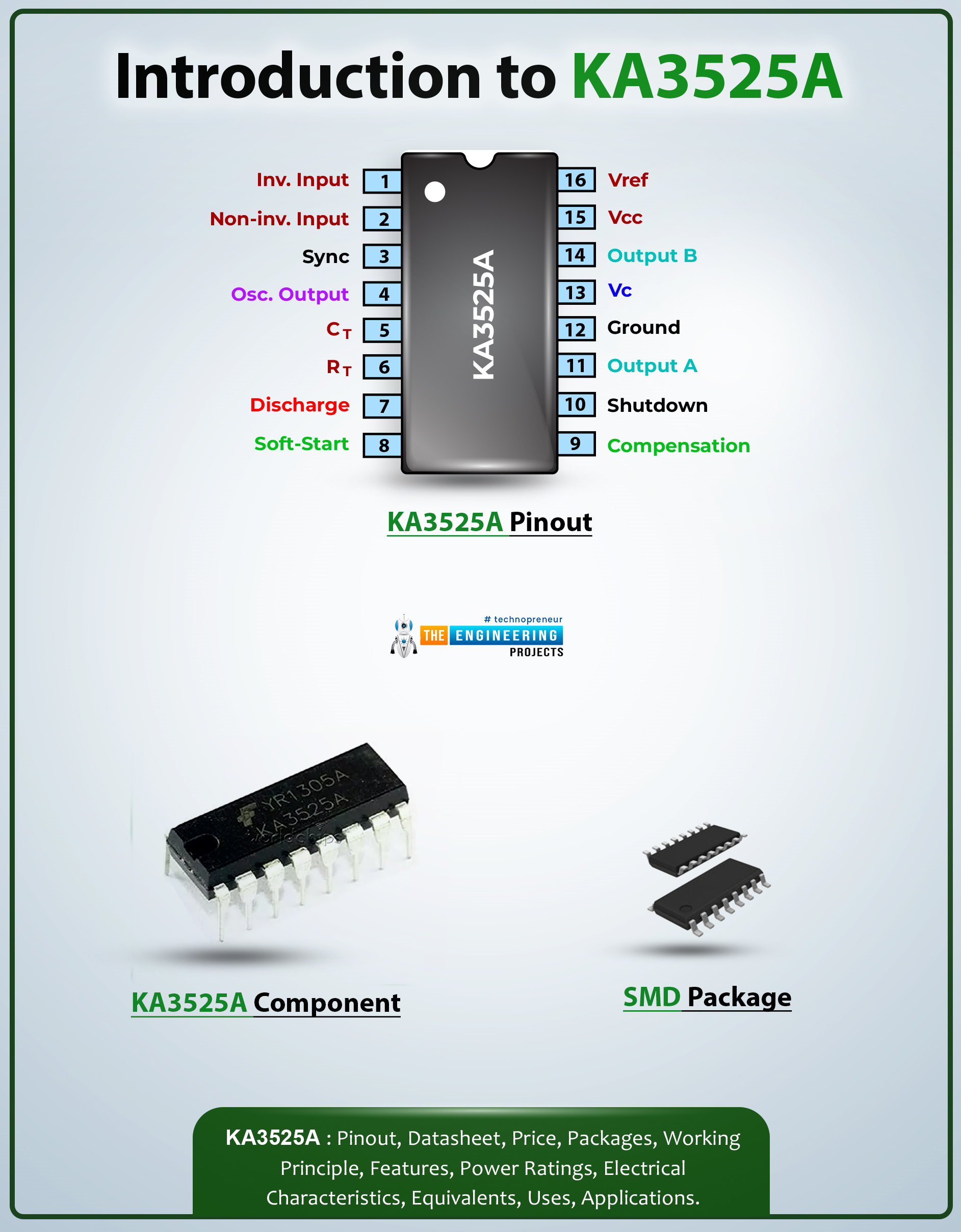
Hi Everyone! I welcome you on board. Happy to see you around. In this post today, I’ll walk you through the Introduction to KA3525A.

The KA3525A is a monolithic IC chip that features the control circuitry mainly required for a pulse width modulating regulator. This device comes with an error amplifier, voltage reference, pulse width modulator, an under-voltage lockout, an oscillator, the output driver, and a soft start circuit, all in one package.

I suggest you buckle up as I’m going to discuss the complete introduction to KA3525A covering datasheet, pinout, features, and applications. Let’s jump right in.

Introduction to KA3525A

  • The KA3525A is a monolithic IC chip that incorporates the control circuitry used for pulse width modulation.
  • During the PWM process, the control circuit inside the chip generates variable-width pulses against the amplitude of the input analog signal.
  • The PWM is a technique that reduces the power produced by the electrical signal by converting it into discrete several parts. Thus, controlling the value of current or voltage by the switch. This switch is located between the supply & load and controls the value of the input signal when we turn it ON and OFF at a fast rate.
  • The term duty cycle is associated with this PWM which is defined as the proportion of ON time of the entire input signal. If the signal remains 10% ON and 90% OFF, then the duty cycle tends to be 10%. If the signal remains 50% OFF and 50% ON, then the duty cycle is said to be 50%.
  • This is a 16-pin chip that requires a supply voltage of around 40V and features a reference output current of around 50mA.
  • The operating temperature ranges from 0 to 70 C while the storage temperature ranges from -65 to 150 C.
  • Power dissipation is 100mW and the output sink current is 500mA.
  • This pulse-width modulation regulator IC incorporates 16 pins.
  • This device generates two PWM signals that are a complement to each other.
  • This component is widely used in switch-mode power supply and other electronic circuits.
  • The output voltage is controlled by feedback circuitry that does it by comparing the feedback signal with a reference voltage.
  • This device features a shutdown protection circuit that turns off the PWM signal if the feedback signal reaches its limit.

KA3525A Datasheet

Before you use this device in your electrical project, it’s better to go through the datasheet of the device that features the main characteristics of the component. Click the link below to download the datasheet of KA3525A.

KA3525A Pinout

The following figure shows the pinout diagram of KA3525A.

  • Pin 1 represents the inverting pin and pin 2 represents a non-inverting pin.
  • If the voltage on the non-inverting pin is less than the voltage on the inverting pin, then the respective duty cycle increases.
  • Pin 3 is employed for the synchronization of two waves while Pin 4 is the output pin of an oscillator.
  • Pins 5, 6 & 7 are incorporated to adjust the frequency of PWM.
  • We can control the frequency of PWM by controlling the value of the discharge resistor, CT capacitor, and RT resistor.
  • Pin 8 SS is a soft start pin that enables the output signal after some time. The value of capacitance is directly related to the soft-start time.
  • Pin 9 is called a compensation pin employed to prevent rapid fluctuations in the output voltage signal.
  • Pin 10 is known as a shutdown pin. It shuts down the PWM signal when the current reaches its limit.
  • Pins 11 and 14 are known as the output pins used to provide input to the MOSFETs. KA3525A incorporates a built-in MOSFET driver circuit.
  • Pin 13 and 15 are called the power pins. Vc should range from 5-35 volts while Vin should stand between 8-35 volts.
  • Pin 16 is known as the reference pin used to adjust the reference voltage through pin 1 or 2.

KA3525A Features

The following are the main features of KA3525A.

  • Carries under-voltage lockout.
  • Available with Oscillator Sync Terminal.
  • Comes with 5V ± 1% Reference.
  • Comes with Deadtime Control.
  • Features Internal Soft Start.

KA3525A Applications

  • It is employed in consumer power electronics applications such as pure sine wave inverters.
  • Used to generate a regulated voltage in a boost converter and a buck converter.

That’s all for today. I hope you enjoyed reading this post. If you have any questions, you can pop your query in the section below, I’d love to assist you the best way I can. You’re most welcome to share your valuable suggestions and feedback about the content we share so we keep sharing quality content customized to your exact needs and requirements. Thank you for reading the article.

CA3130 MOSFET Op-Amp Datasheet, Pinout, Features & Applications

Hello Friends! Hope you’re well today. I welcome you on board. Thank you for clicking this read. In this post today, I’ll detail the Introduction to CA3130.

The CA3130 is a BiMOS Operational Amplifier that comes with MOSFET. BiMOS is a term that defines the combination of both CMOS and bipolar op-amp technology into a single integrated circuit. CMOS op-amp is highly efficient and consumes less current while bipolar op-amp carries high bandwidth. Overall CA3130 is a device that combines the advantages of both bipolar and CMOS op-amp means it consumes less power and carries high bandwidth.

I suggest you buckle as I’ll discuss the complete Introduction to CA3130 covering datasheet, pinout, features, and applications. Let’s get started.

Introduction to CA3130

  • The CA3130 is a BiMOS Operational Amplifier that incorporates MOSFET. It is widely used in Mobile jammers and oscillator circuits.
  • Incorporated in a frequency generator, CA3130 carries an input terminal current of around 1mA and a maximum output voltage of around 13.3V.
  • The common-mode rejection ratio of this device is 80 dB. This rejection ratio is the ability of the device to turn down common-mode signals. It is a ratio between differential mode gain and common-mode gain.
  • The CA3130 comes with high input impedance due to the presence of built-in MOSFETs. This also projects when the output voltage of the sensor is attached to the non-inverting and inverting pin of the op-amp, the resulting output voltage of the sensor doesn’t change its value.
  • If you are pondering for a device with less power consumption, fast sample rate, high input impedance, and high bandwidth, then this CA3130 op-amp might be the right fit for you.

How to Use CA3130

  • CA3130 carries both inverting and non-inverting pins.
  • The non-inverting pin is directly related to the inverting terminal and the output pin means when the voltage at the non-inverting pin is high then both the inverting pin and output pin will be high.
  • The CA3130 operates as a single supply voltage with a range of 5V to 16V and as a dual supply mode with a range of ±2.5V to ±8V.
  • Here in this example, we will take a single supply voltage with a power supply of 5V, as this is the most commonly used circuit.
  • In this circuit design, the pin 8 Vcc is attached to the 5V voltage supply while pin 4 is grounded where the potential difference is zero. A sample CA3130 circuit is given below.
  • The rise time of this device is 0.09uS and the CMRR is 80dB which makes it an ideal pick for voltage followers and high-frequency applications.

CA3130 Datasheet

Before you install this component in your project, it’s wise to scan through the datasheet of the component that details the main characteristics of the device. Click the link below and download the datasheet of CA3130.

CA3130 Pinout

The following table exhibits the pin description of CA3130.

Absolute Maximum Rating of TL081
Pin No. Rating Symbol
1 Used to set the offset voltage Offset Null Pin
2 A fixed voltage is applied to this pin Inverting Pin IN -
3 A variable voltage is applied to this pin Non-inverting Pin IN +
4 Ground (zero potential difference) Vcc -
5 Used to set the offset voltage Offset Null Pin
6 The output pin of the op-amp Output
7 Voltage supply pin that gets voltage range 5 to 16V Voltage supply pin Vcc+
8 Used to turn off the output stage Strobe

The following figure represents the pinout diagram of CA3130.

  • Pin 4 is the ground pin while pin 7 is the voltage supply pin.

CA3130 Features

  • Sink current Max. = 20mA
  • Input Terminal current = 1mA
  • Common Mode Rejection Ratio (CMRR) = 80dB
  • Comes with a wide power supply range
  • Singe supply – 5V to 16V
  • Dual supply – ±2.5V to ±8V
  • Maximum Output Voltage = 13.3V
  • Op-amp incorporated with MOSFET at the output
  • Source current Max. = 22mA
  • Supply current = 10mA

CA3130 Applications

  • Incorporated in mobile jammers
  • Employed in Oscillator circuits
  • Employed in DAC circuits
  • Used in voltage follower circuits
  • Used in Peak Signal/Noise detectors
  • Used in frequency generator/distorter

That’s all for today. Hope you enjoyed reading this article. If you’re unsure or have any questions, you can approach me in the comment section below, I’d try to help you according to the best of my expertise. Feel free to leave your valuable suggestions or feedback about the content we share so we keep sharing quality content customized to your exact needs and requirements. Thank you for reading this post. Stay tuned!

SB560 Schottky Diode Datasheet, Pinout, Features & Applications

Hi Friends! Hope you’re well today. I welcome you on board. Thank you for clicking this read. In this post today, I’ll detail the Introduction to SB560. The SB560 is a Schottky diode, also known as a hot-carrier diode, mainly incorporated in extremely fast switching applications. It comes with low forward drop voltage and is used in the high-frequency operation. A highly reliable and efficient device, SB560 is a high forward surge capability component available in the DO-201AD package. This device carries a maximum RMS voltage of 42V while the maximum repetitive peak reverse voltage is 60V. I suggest you go through this entire post till the end, as I’ll detail the Introduction to SB560 covering datasheet, pinout, features, and applications. Let’s jump right in.

Introduction to SB560

  • The SB560 is a Schottky diode used in extremely fast switching applications. It is also known as a hot-carrier diode.
  • When semiconductor material combines with the metal, they generate Schottky diode. This diode is a two-terminal device where these terminals are used for the external connection with the circuit.
  • One terminal is known as anode made of metal material while the other terminal is called cathode made of semiconductor material.
  • The anode side is positive while the cathode side is negative. And current only flows in one direction. This diode blocks the current in the opposite direction. The current flows from the anode pin to the cathode pin.
  • This Schottky diode is also known as a hot-carrier diode. In an unbiased condition, this device possesses low electronic energy that results in the construction of a barrier that restricts the movement of electrons. Due to the formation of this barrier, Schottky diodes are also called hot-carrier diodes.
  • Schottky diode and common diode operate in a similar fashion considering the flow of current. Both favor current flow in one direction and restrict the current flow in another direction. These devices are different considering the voltage required to power up these diodes.
  • Though both devices require 2V DC source voltage, the Schottky diode needs only 0.3V, leaving behind 1.7V to supply power to the diode. While common diode needs only 0.7V, leaving behind 0.3V to supply power to the diode.

SB560 Datasheet

While working with the electrical devices, it’s better to go through the datasheet of the component that details the main characteristics of the component. You can easily download the datasheet of this component SB560 by clicking the link below.

SB560 Pinout

The following figure shows the pinout diagram of SB560. The SB560 is made of two terminals called anode and cathode. The anode side is positive while the cathode side is negative. Current flows from the anode terminal to the cathode terminal.

SB560 Features

  • Applied for over-voltage protection
  • High current capability device
  • High surge current capability device
  • Polarity = Cathode band
  • average forward rectified current = 5A
  • Package = DO-201AD
  • Maximum RMS voltage = 42V
  • Mounting position = Any
  • Repetitive peak reverse voltage = 60V
  • Comes with low forward voltage drop
  • Low power loss and highly efficient device
  • Low cost and high-reliability device

SB560 Schottky Diode Construction

  • Schottky diode is formed when the semiconductor material is joined with metals like tungsten, platinum, chromium, and molybdenum.
  • When these two materials are joined they constitute a barrier that blocks the movement of electrons.
  • Recall, the formation of a barrier is due to the low electronic energy in the unbiased condition.
  • Commonly, the n-type semiconductor material is used to form the Schottky diode.
  • P-type semiconductor materials are also used for making the Schottky diode but they are not preferred over n-type semiconductor materials because the former comes with low forward drop voltage.
  • The anode side of the diode is composed of metal while the cathode side is made of semiconductor material. And current flows from the positive anode side to the negative cathode side.

SB560 Applications

  • Used in low voltage inverters and DC/DC converters.
  • Used to control the electronic charge.
  • Used in freewheeling and logic circuits.
  • Used for signal detection.
  • Used in polarity protection and high-frequency applications.
  • Used in sample-and-hold circuits.
  • Used in solar systems and radio frequency applications.
  • Used for extremely fast switching applications.
That was all about the Introduction to SB560. I hope you find this article useful. If you’re unsure or have any question, you can ask me in the comment section below, I’d love to help you the best way I can. You’re most welcome to share your valuable suggestions around the content we share so we keep producing quality content. Thank you for reading the article.

FR107 Fast Recovery Diode Datasheet, Pinout, Features & Applications

Hello Everyone! Hope you’re well today. Happy to see you around. In this post today, I’ll walk you through the Introduction to FR107.

Fr107 is a fast recovery diode mainly used for converting alternating current to direct current. It can support loads under 1A and carries a peak inverse voltage of 1,000 V.

Read this post all the way through as I’ll detail the complete Introduction to FR107 covering datasheet, pinout, features, characteristics, and applications. Let’s get started.

Introduction to FR107

  • Fr107 is a fast recovery diode mainly used in fast-switching applications. It comes with two terminals called an anode and a cathode. The grey-colored band identifies the cathode side while the other side is the anode.

  • A highly efficient and reliable device, FR107 comes with a low forward drop voltage.
  • It’s a high-current capability device that weighs 0.33 grams.

The diode conducts in forward biased condition and blocks the current in reverse biased condition. When the diode steps into the reverse biased condition from the forward biased condition, it supports the flow of current for a few nanoseconds. The diode reverse recovery time is defined as the time taken by the diode to regain its blocking capability in the reverse biased condition where it doesn’t support the flow of current. The reverse recovery time of this diode is 500ns.

FR107 Datasheet

Before you apply this component to your electrical project, it’s better to go through the datasheet of the component that details the main characteristics of the component.

Click the link given below and download the datasheet of FR107:

FR107 Pinout

The following figure shows the pinout diagram of FR107.
  • This tiny component is composed of two terminals named anode and cathode terminal. The anode pin is positive and the cathode pin is negative. The current enters the diode from the anode pin and it leaves the diode from the cathode pin. Moreover, current flows from the anode pin to the cathode pin.
  • The cathode pin can be identified with the grey-colored band on it. And the other side is called the anode.
  • The following figure shows the electrical symbol of the FR107.
  • The triangle side with the line is called the cathode while the other side is the anode.

FR107 Features  

  • Package = DO-41
  • Low forward voltage drop
  • Used for fast-switching applications
  • Highly efficient
  • Comes with high Reliability and low Leakage
  • High current capability device
  • Weight = 0.33 grams

FR107 Characteristics

  • Polarity = Cathode band
  • Recurrent Peak Reverse Voltage Max. = 1000 V
  • Reverse recovery time = 500 ns
  • Typical Junction Capacitance = 15 pF
  • Average Forward Output Current Max. = 1 A
  • Forward Voltage Drop per element at 1.0A DC Max = 1.3 V
  • Operating and Storage Temperature Range = -65 to 150 °C

FR107 Applications

  • Used in fast-switching applications.
  • Supports loads under 1A.
  • Mixing signals.
  • Isolating signals from a supply.
  • Controlling the size of a signal.

That’s all for today. I hope you find this article helpful. If you have any questions, you can approach me in the section below. I’d love to help you the best way I can. Feel free to share your valuable suggestions around the content we share so we keep producing quality content customized to your exact needs and requirements. Thank you for reading the article.

FR106 Fast Recovery Diode Datasheet, Pinout, Features & Applications

Hello Everyone! I welcome you on board. Hope you’re well today. In this post today, I’ll detail the Introduction to FR106.

The Fr106 is a fast recovery diode mainly employed in fast-switching applications. It supports loads under 1A and carries a peak inverse voltage of 800 V.

I suggest you read this post all the way through as I’ll walk you through the complete Introduction to FR106 covering datasheet, pinout, features, characteristics, and applications. Let’s jump right in.

Introduction to FR106

  • Fr106 is commonly known as a fast recovery diode mainly employed in fast-switching applications. This is a two-terminal device named anode and cathode.
  • The gray-colored band at one side of the diode indicates the cathode side while the other side is the anode terminal.

  • FR106 is a highly efficient and reliable device. Plus, it carries a low forward drop voltage. It’s a high-current capability device that weighs 0.35 grams.
  • The diode conducts in one direction only i.e. from anode to cathode in forward biased condition and it doesn’t support the flow of current in the opposite direction in reverse biased condition.
  • When diode conducting in forward biased condition switches to reverse condition… it, for a split second, favors the flow of current due to its forward-biased condition. This is called the diode reverse recovery time which is termed as the time required for the diode to regain its blocking ability in the reverse biased condition.
  • The reverse recovery time, in this case, is 250 ns.

FR106 Datasheet

Before you employ this component in your project, it’s wise to scan through the datasheet of the component that highlights the main characteristics of the component.

You can download the datasheet of FR106 by clicking the link below.

FR106 Pinout

The following figure represents the pinout diagram of FR106.

  • FR106 comes with two pins called anode and cathode. These pins are also named as terminals that are used for external connection with the electrical circuit.
  • The anode pin is positive and is the area from where current enters the diode while the cathode pin is negative and is the place from where current leaves the diode.
  • The current moves in one direction only in the diode i.e. from the anode terminal to the cathode terminal.
  • The following figure shows the electrical symbol of FR106.

The line on the triangle represents the cathode terminal while the anode side is the anode terminal.

FR106 Features 

  • Package = DO-41
  • Used for fast switching applications
  • Carries low forward voltage drop and highly efficient
  • Comes with high Reliability and low Leakage
  • High current capability device
  • Weight = 0.35 grams

FR106 Characteristics

  • Polarity = Cathode band
  • Reverse recovery time = 250 ns
  • Forward Voltage Drop per element at 1.0A DC Max = 1.3 V
  • Recurrent Peak Reverse Voltage Max. = 800 V
  • Average Forward Output Current Max. = 1 A
  • Typical Junction Capacitance = 15 pF
  • Storage and Operating Temperature Range = -65 to 150 °C

FR106 Applications

  • Supports loads under 1A.
  • Mixing signals.
  • Used in fast switching applications.
  • Controlling the size of a signal.
  • Isolating signals from a supply.

That’s all for today. I hope you enjoyed this article. If you’re unsure or have any questions, you can pop your comment in the section below. I’d love to help you the best way I can. Feel free to share your valuable suggestions and feedback, they help us create quality content. Thank you for reading the article.

TL084 Op-Amp Datasheet, Pinout, Feature & Applications

Hi Guys! Hope you’re well today. I welcome you on board. Happy to see you around. In this post today, I’ll detail the Introduction to TL084. TL084 is a JFET input Op-Amp that carries low offset current and high input impedance. Available with better offset characteristics and high noise immunity, TL084 comes with a suitable offset voltage that makes it an ideal pick for amplifier applications. I suggest you read this post all the way through as I’ll walk you through the complete Introduction to TL084 covering datasheet, pinout, features, and applications. Without further ado, let’s get started.

Introduction to TL084

  • The TL084 is available in Quad Package which means it comes with four separate op-amps that can operate independently.
  • This op-amp carries low noise and harmonic distortion that makes it an ideal pick for the audio pre-amplifiers.
  • The bipolar transistors and high-voltage JFET are incorporated that are responsible for the device's low bias current and high input impedance.
  • Previously, I’ve uploaded Introduction to LM324 op-amp that is almost similar to TL084 as both are available in quad package and carry four op-amps inside.
  • Both operate in a similar manner, however, the area where they differ is the voltage required for the working of these op-amps. The TL084 requires 7 V for its operation while LM324 requires a common 5V supply to put it in running condition.
  • While using TL084, make sure you terminate the unused op-amp in this Quad package. Since, if not terminated, they might develop some stay capacitance that can get some noise, hence affecting the overall performance of this device.
  • Moreover, unused op-amp utilizes more power, thus decreasing the device efficiency.

TL084 Internal Design

  • Op-amps are famous for their high input impedance which means it doesn’t distort the initial signal applied to the input pin.
  • The op-amp input stage is considered as the most complex stage of the amplifier, because if handled inappropriately, it may result in the damage of the entire circuitry.
  • While working with the supply voltage signals make sure, the voltage applied to the input pin should never exceed the rail voltage else it will generate a short circuit by producing the latch-up condition.
  • Moreover, the differential input voltage rating must be higher than the voltage difference between the inverting and non-inverting pins.
  • It is important to note that TL084 is not a rail to rail op-amp which means output voltage will not be reaching the maximum negative or maximum positive value when the device is saturated.
  • You will always get the 2V less than the supply voltage due to the voltage drop occurred by the transistors inside the op-amp.
  • Op-amps carry a very large open-loop gain but this gain is commonly occupied with the noise, the reason most circuits are designed using closed-loop gain.
  • The closed-loop gain works in such a way it keeps feeding the input signal with the feedback signal which results in the restriction of gain value and the noise accompanied by it.
  • Know that… negative feedback is preferred over positive feedback due to its stable and predictable behavior.

TL084 Datasheet

While incorporating this device into your electrical project, it’s wise to have a look at the datasheet of the component that details the main characteristics of the component. You can download the datasheet of TL084 by clicking the link below.

TL084 Pinout

The following are the 14 pins embedded in this op-amp.
Absolute Maximum Ratings BC639
Pin No. Rating Pin name
4 Power supply Vcc(+)
13 Ground GND
3,5,10,12 The input non-inverting pins of this Quad Op-amp Input non-inverting Pins
2,6,9,13 The input inverting pins of this Quad Op-amp Input inverting pins
1,7,8,14 The output pins of the this Quad Op-amp Op-amp output pins
  • The following figure shows the pinout diagram of TL084.
  • Pin 4 is the positive supply rail of the op-amp while pin 13 is the negative supply rail of the op-amp.

TL084 Features

The following are the main features of TL084.
  • Operating Voltage Min. = 7V
  • Input Bias Current = 20pA
  • JFET Input Op-Amp Quad Package
  • Input Offset Voltage = 3mV
  • Common mode rejection ratio (CMRR) = 86dB
  • Typical operating voltage range = +18V to -18V
  • Available in SO-14, 14-pin PDIP, TSSOP packages
  • Gain = 200 V/mV
  • Used for output short circuit protection
  • Carries bandwidth = 4MHz

TL084 Applications

  • Employed in amplifier circuits.
  • Employed in audio pre-amplification.
  • Used in audio/noise filter circuits.
  • Used in buffer application.
  • Incorporated in multi-stage voltage generators.
  • Used in a circuit requiring high input impedance.
That’s all for today. I hope you find this article helpful. If you have any questions, you can ask me in the section below, I’d love to help you the best way I can. Share your valuable suggestions and feedback around the content we share, so we keep producing quality content customized to your exact needs and requirements. Thank you for reading the article.

TL081 Op-Amp Datasheet, Pinout, Feature & Applications

Hi Guys! Hope you’re well today. I welcome you on board. Happy to see you around. In this post today, I’ll detail the Introduction to TL081.

TL081 is a high-speed general-purpose JFET input single operational amplifier that comes with high noise immunity and better offset characteristics. It carries high input impedance and low offset current. The offset voltage of this device makes it an ideal match for amplifier applications. It incorporates well-matched bipolar transistors and high-voltage JFET in a compact IC.

Read this post till the end as I’ll detail the complete Introduction to TL081 covering datasheet, pinout, features, and applications. Let’s jump right in.

Introduction to TL081

  • TL081 is a high-speed JFET input single operational amplifier that comes with high slew rates, and low offset and input bias currents.
  • It features a low offset voltage temperature coefficient with a supply voltage of around +-18V and an input voltage of around +-15V.
  • Plus, it incorporates internally trimmed offset voltage and needs low supply current
  • It has the ability to maintain a fast slew rate and a large gain bandwidth.

TL081 Datasheet

Before you incorporate this device into your electrical project, it is wise to have a look at the datasheet of the device that features the main characteristics of the component. Click the link below and download the datasheet of TL081.

TL081 Pinout

There are a total of 8 pins incorporated in this op-amp as described below.

Absolute Maximum Ratings TL081
Pin No. Description Pin Name
1,5 Used to set the offset voltage
2 Inverting Input IN -
3 Non-inverting Input IN +
4 Ground GND
6 Output Output
7 Voltage Supply Vcc
8 Not connected NC

The following figure shows the pinout diagram of TL081.

Out of 8 pins on the integrated circuit, 7 are associated with particular functions while one pin (pin no. 8) is not connected.

TL081 Features

The following are the main features of TL081.

  • Wide differential and common-mode voltage range
  • Low input bias and offset current
  • Input Bias Current = 200pA
  • GBP - Gain Bandwidth Product = 3 MHz
  • Latch-up free operation
  • High slew rate = 16 V/us
  • Supply Voltage: 7V to 36 V
  • Power Dissipation = 670mW
  • Available with internal frequency compensation
  • CMRR - Common Mode Rejection Ratio = 70 dB to 86 dB
  • Output short-circuit protection
  • High input impedance
  • Operating Supply Current = 1.4 mA
  • Comes in 8-pin PDIP, SOIC Packages

TL081 Absolute Maximum Ratings

The following table shows the absolute maximum ratings of TL081.

Absolute Maximum Ratings TL081
No. Rating Symbol Value Unit
1 Supply Voltage Vcc +-18 V
2 Input Voltage Vin +-15 V
3 Differential Input Voltage Vid +-30 V
4 Power Dissipation Ptot 680 mW
5 Output short-circuit duration Infinite
6 Available Package PDIP, SOIC Packages
7 Storage Temperature Range Tstg -65 to 150 C
  • The values of all voltages, excluding differential voltage, are measured with respect to the ground of the supply voltages where the midpoint between VCC+ and VCC- is a zero reference level.
  • It is important to note that the input voltage magnitude should never cross the supply voltage magnitude. The supply voltage here, in this case, is +-18V while the magnitude of the input voltage is +-15V.
  • Power dissipation is 680mW and the storage temperature range is -65 to 150C.
  • Differential voltages are considered as the non-inverting input terminal with respect to the inverting input terminal.
  • Moreover, the output is shorted to ground or to either supply. Temperature and/or supply voltages must be in control so the dissipation rating is not exceeded.
  • Short-circuits can cause destructive dissipation and excessive heating.

TL081 Applications

  • Incorporated in audio pre-amplification.
  • Used in amplifier circuits.
  • Used in circuit requiring high input impedance.
  • Sample and Hold Amplifiers
  • Peak Detectors
  • Active Filters
  • Comparators
  • Function Generators

That’s all about the Introduction to TL081. I hope you find this article helpful. If you’re unsure or have any questions, you can approach me in the section below, I’d love to help you the best way I can. Share your valuable suggestions and feedback around the content we share, they help us generate quality content customized to your exact needs and requirements. Thank you for reading the post.

Syed Zain Nasir

I am Syed Zain Nasir, the founder of <a href=https://www.TheEngineeringProjects.com/>The Engineering Projects</a> (TEP). I am a programmer since 2009 before that I just search things, make small projects and now I am sharing my knowledge through this platform.I also work as a freelancer and did many projects related to programming and electrical circuitry. <a href=https://plus.google.com/+SyedZainNasir/>My Google Profile+</a>

Share
Published by
Syed Zain Nasir