Interfacing Arduino with HC-05

Hello friends, i hope you all are fine and enjoying. Today i am going to share a new tutorial which is Interfacing Arduino with HC05 Bluetooth module. First of all lets have a little introduction about HC-05 Bluetooth module. HC-05 is a bluetooth module, which was designed for wireless data communication. This little module is capable of both sending and receiving data but it performs only one thing at a time, which means at a particular time it can only send or receive data but can't do the both tasks.

In order to send or to receive data, you have to make one module as a master and the other module as a slave. If both the modules are acting as master then, data will not transmit and if both the modules are acting as a slave then, again data will not transmit or receive. The hardware of Bluetooth module contains a large no of features. For example it is much sensitive and it is sensitive up to -80dBm and it catches a Bluetooth signal even from far away. If you wish to transmit data through it then, it also have much power to transmit data to a wider range. You can image its transmitting power from the digits that it has transmitting power of +4dBm. This module operates on a low voltages, that's why the power rating of this module is very low. The hardware of the module comes with a integrated antenna and also its hardware contains edged pins. These edged pins gives us the ease that it becomes very easy to plug in or plug out the wires. and also if you are going to use it within a circuit then, it becomes very easy to connect the cable with module. Above was a little introduction about Bluetooth module and its features. now lets move to the basic theme of our project, which is to do interfacing between arduino and HC-05.

Note:

  • If you have HC-06 or any other module in HC series then you don't need to get worried as they all work quite same. So you can also follow this tutorial for other HC series bluetooth modules.

Pin Configuration of HC-05

HC-05 Bluetooth module has total 6 pins. A simple HC-05  Bluetooth module is shown in the image given below and you can also see its pin configuration from this image. The pin configuration and the purpose of each pin is listed below as:

  1. They pin#1 is abbreviated a KEY pin. The function of this key is to show paired devices. In HC-05 module this pin is used to perform the module in AT mode.
  2. Pin#2 of HC-05  module is named as VCC pin. This module requires 3.3 volts to operate. If you will connect it directly with 5 volts then, this module will burn out.
  3. Pin#3 of this module is named as GND. At this pin the common ground of the circuit is provided.
  4. pin#4 is named as TXD. This pin is used when you have to transmit data to some external device. Asynchronous data transfer is performed by this module.
  5. pin#5 is named as RXD. This pin is used when the module have to receive wireless data from some external source. Asynchronous data is received through this module.
  6. The last pin of the module which is in fact pin#6 of the module and it is named as STATUS pin. The basic function of this pin is to check the status of the Bluetooth module. If the module is connected to some other device then, output of the system becomes HIGH and if the connection of Bluetooth drops then, this module generates a output pulse.

Interfacing with Arduino

So, now let's start with interfacing Arduino with HC05 bluetooth module. Its quite easy to interface as it works on Serial protocol. As mentioned above it has two pins named as TX and RX through which we can send or receive the data. Moreover, it works exactly the same as any mobile's bluetooth, you can connect your mobile with any device and can share data between these devices, similarly you can share the data with this device as well.
  • First of all, connect your HC05 bluetooth module with Arduino as shown in the below figure.
  • In the above figure, the connections are quite easy , we have provided power to the bluetooth module from Arduino and also connected TX pin of bluetooth module with RX pin of Arduino and RX pin of bluetooth module with TX of Arduino.
  • Now we are done with the connections so next part is to upload the code into Arduino.

Code for interfacing HC-05 with Arduino

Now upload the below code into your Arduino and you are ready to get the first data from your Bluetooth module.

Applications of HC-05 Module

  • The biggest application is that it is used to transmit or receive data wirelessly.
  • You can play your favorite sound tracks through bluetooth in your car using this module.
  • The modern Android phones contains a wireless GPS option. IN fact this module is being used in that phones and it works to seek the bluetooth location.
  • This module makes you able to chat with some android phone using Bluetooth.
Alright friends, that all for today. If you have any question, fell free to ask. Till next tutorial Take Care!!! :)

JRC4558 Op-Amp Datasheet, Pinout, Features, Alternatives & Applications

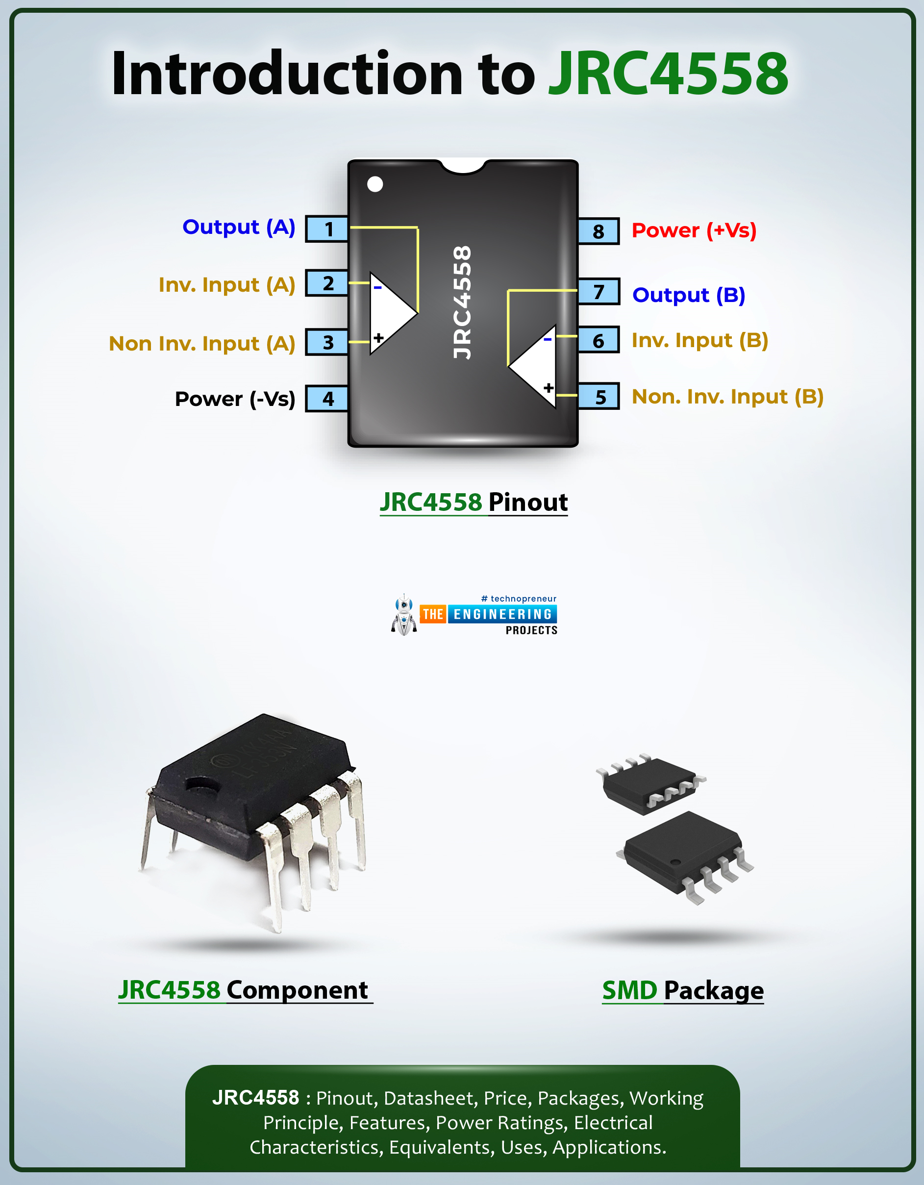
Hi Guys! Happy to see you around. I welcome you on board. Thank you for clicking this read. In this post today, I’ll walk you through the Introduction to JRC4558.

The JRC4558 is a single silicon-chip monolithic dual operational amplifier. This amplifier is a high-performance device and is internally compensated. It is widely used in sample and hold amplifiers and pedal circuit designs. The JRC4558 is available with a remarkable input impedance of around 5 MO, a high voltage gain of around 100 dB, and a good slew rate of around 1.7V/µs.

I suggest you buckle up as I will walk you through the complete introduction to JRC4558 covering datasheet, pinout, features, alternatives, and applications. Let’s jump right in.

Introduction to JRC4558

  • The JRC4558 is a single silicon-chip monolithic dual operational amplifier that comes with high voltage gain and good input impedance.
  • It is applied in portable instrumentation and Intrusion Alarm Systems.
  • There are a total of eight pins incorporated on the device, where PIN 8 is the voltage supply pin and pin no 4 is the ground pin. And you’ll get two outputs at the same time.
  • There are two inputs i.e. input A and input B and both inputs contain one inverting input (-) with Voltage V- and non-inverting input (+) with voltage V+.
  • The ideal op-amps are different from the real op-amps used in this chip. The ideal op-amp comes with infinite gain while the voltage gain of this device is finite and is around 100dB.
  • The slew rate of this device is around 1.7V/µs which is achieved when the output voltage of the amplifier reaches its maximum rate of change.
  • This chip is incorporated with two independent, good input impedance and internally frequency compensated operational amplifiers that are carefully designed to run over a wide range of voltages from a single power supply.
  • The JRC4558 produces an output signal that is much larger than the potential difference at the input.
  • It is also applied in general-purpose operational amplifier circuits like differential amplification, comparators, and mathematical operations.
  • This device is carefully designed and requires only a 5V standard voltage supply to operate in electronic circuits. You don’t need to include an additional -5V supply to run this device.
  • Moreover, it is also employed in single-supply voltage systems, amplification blocks, and transducer amplifiers.
  • This device is capable of performing two different operations at the same time as it incorporates two op-amps on board.
  • The versatility of this device makes it a good pick for analog circuits.
  • It is widely used in scientific devices and industrial and consumer applications.
  • This device can be used individually or as a component of most complex integrated circuits.

JRC4558 Datasheet

Before applying this device to your electrical project, it’s wise to go through the datasheet of the component that contains the main characteristics of the component. Click the link below and download the datasheet of JRC4558.

JRC4558 Pinout

The following figure shows the pinout diagram of JRC4558.

The JRC4558 comes with a total of 8 pins as mentioned below in the table.

Pin Description of JRC4558
Pin No. Pin Description Pin Name
1 The output pin of Op-amp A OUT (A)
2 The Inverting input pin of the Op-Amp A Inverting Input (A)
3 The Non-Inverting Input Pin of Op-Amp A Non- Inverting Input (A)
4 Ground or Negative supply terminal Power (-Vs)
5 The non-inverting Input Pin of Op-Amp B Reference
6 The Inverting input pin of the Op-Amp B Output
7 The output pin of Op-amp B Power (+Vs)
8 Positive supply terminal +VS

JRC4558 Features

The following are the main features of the JRC4558.

  • No. of Amplifiers = 2
  • Voltage Gain = 100 dB
  • Device Slew Rate = 1.7V/µs
  • Input Impedance = 5 MO
  • Available Bandwidth = 3MHz
  • Operating Temperature Max = 70°C
  • Supply Voltage Range = ± 5V to ± 15V
  • of Pins on the component = 8
  • Operating Temperature Min = 0°C
  • Available Package = 8-Pin DIP and SOP Package

JRC 4558 Alternatives

The following are the alternatives to JRC4558.

  • LM158
  • LM358
  • LM358A
  • LM2904Q
  • LM158A
  • LM2904
  • LM747
  • LM4558

JRC4558 Applications

The JRC4558 is used in the following applications.

  • Applied in Sample and Hold Amplifiers
  • Used in Portable Instrumentation
  • Employed in Instrumentation Amplifiers
  • Used in Long-Duration Timers/Multivibrators
  • Incorporated in Intrusion Alarm System
  • Employed in Photocurrent Instrumentation
  • Used in Comparators and Function Generators

That’s all for today. I hope you’ve enjoyed reading this article. If you are unsure or have any queries, you can pop your question in the section below. I’d love to help you the best way I can. Feel free to share your valuable suggestions and feedback around the content we share, so we keep sharing quality content customized to your exact needs and requirements. Thank you for reading the article.

LM2576 Buck Converter Datasheet, Pinout, Features & Applications

Hi Everyone! I welcome you on board. Thank you for clicking this read. In this post today, I’ll walk you through the Introduction to LM2576.

LM2576 is a step-down voltage regulator, also known as a buck converter, mainly employed as a pre-regulator in linear regulators. The customized output version of this buck converter gives you the ability to set the output voltage as you like better. It is available with a remarkably good load and line regulation. Moreover, it is used to drive load under 1A and is available in fixed output voltages with 3.3V, 5V, 12V, and 15V.

I suggest you buckle up and read this post all the way through, as in this post I’ll detail the Introduction to LM2576 covering the datasheet, pinout, features, and applications. Let’s jump right in.

Introduction to LM2576

  • LM2576 is a voltage regulator, also called a buck converter, mainly used as a pre-regulator in linear regulators.
  • It is a simplified version of switching power supplies where it houses all functions needed to step down the circuit voltage.

  • This buck converter comes with an integrated switch that drives load under 1A.
  • LM2576 is available with remarkable load regulation and load line.
  • LM2576 is available in two versions: version with fixed output voltage featuring 3.3V, 5V, 12V, & 15V and version with adjustable output that comes with the ability to choose your desired output.
  • It is also known as the DC-to-DC power converter mainly used to step down the voltage from the input supply to its output load. The current is increased during this occurrence of voltage regulation.
  • This buck converter comes with a fixed-frequency oscillator of around 52 kHz. It is also available with an in-built frequency compensation method.
  • Frequency compensation is used to minimize the oscillation and vibration in the electrical circuit. Resistance-capacitance networks are applied for this frequency method to work.
  • Apart from the excellent load and line regulation, this component is available with a manual shutdown option using an external ON/OFF pin.

LM2576 Datasheet

Before you apply this component to your electrical project, it’s better to go through the datasheet of the component that features the main characteristics of the device. You can download the datasheet of LM2576 by clicking the link below.

LM2576 Pinout

The following figure shows the pinout diagram of lm2576.

LM2576 is available with five terminals:

  1. ON/OFF: This pin is used to shut down the voltage regulator when the input supply current is decreased to 50uA. The threshold voltage is 1.3V. When the voltage on this pin is set to below the threshold voltage, it will turn on the voltage regulator. When the voltage on this pin goes above the threshold voltage it will turn off the device. And when this pin is connected to the ground or leave it open, it will remove the shutdown feature from the device. Whether you connect this pin to the ground or leave it open, in both cases the regulator remains turned on.
  2. VIN: This pin is connected to the bypass capacitor that reduces the voltage transients along with providing the switching current.
  3. Output: This terminal behaves like an internal switch where voltage potential goes back and forth between (Vin – Vsat) and -0.5V. The Vout/Vin is this pin duty cycle. The coupling is reduced due to the presence of PCB copper attached to this pin.
  4. Ground: This is the ground pin.
  5. Feedback: For the feedback loop, this pin defines the regulated output voltage.

LM2576 Features

The following are the main features of LM2576.

  • Output Voltage available for variable type regulator = 1.23V to 37V
  • Internal Oscillator frequency = 52-kHz (this is a Fixed Frequency)
  • Output Current = 3A
  • Used as a switch-mode step-down voltage regulator
  • Comes with In-built Current Limit and Thermal Shutdown Protection
  • Output Voltage available for fixed voltage regulator = 3.3V, 5V, 12V or 15V
  • Maximum Input Voltage =  40V
  • Available packages = TO-263 & TO-220

LM2576 Applications

The following are the main applications of LM2576.

  • Incorporated as a pre-regulator in linear regulator
  • Used in On-card switching regulators.
  • Employed to drive load under 1A.
  • Employed in a simple efficient step-down regulator.
  • Used in a positive-to-negative converter.

That was all about the Introduction to LM2576. Hope you’ve enjoyed reading this article. If you have any queries, you can pop your question in the section below, I’d love to help you the best way I can. Feel free to share your valuable feedback and suggestions around the content we share, so we keep producing quality content customized to your exact needs and requirements. Thank you for reading the article.

1n4734 Zener Diode Datasheet, Pinout, Features & Applications

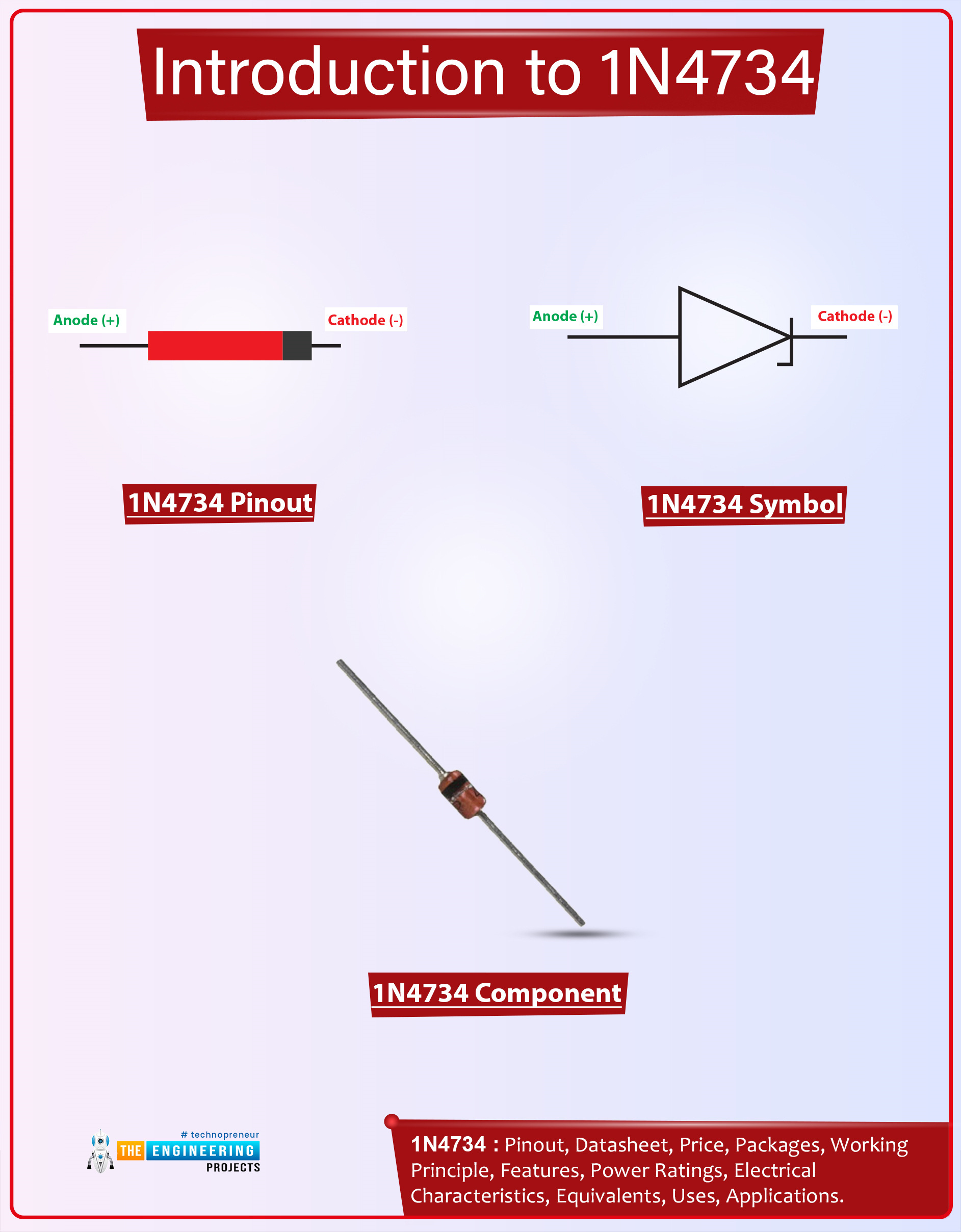
Hi Folks! I hope you’re well today. I welcome you on board. In this post today, I’ll walk you through the Introduction to 1n4734.

The 1n4734 is a silicon planner power Zener diode that is employed as a low current voltage regulator. It is incorporated as a shunt regulator in many applications. This Zener diode conducts the current in both directions in contrast to the regular diode that conducts in one direction only i.e. regular diode conducts in forward biased condition only. This Zener diode conducts in both conditions forward biased condition and reverse biased condition. Power dissipation in this Zener diode is 1W and standard Zener voltage tolerance is ±10%.

I suggest you read this entire post till the end, as I’ll detail the complete Introduction to 1n4734 covering datasheet, pinout, main features, and applications. Let’s dive in.

Introduction to 1N4734

  • The 1n4734 is a Zener diode employed as a low-current voltage regulator. It is also employed in clipping circuits with high power ratings. This Zener diode is made of semiconductors and is used in voltage protection circuits.

  • The current flows from the anode side to the cathode side in the regular diode in a forward-biased condition. On the other hand, in the case of the Zener diode, current conducts in both conditions i.e. forward biased condition and reverse biased condition. Forcing regular diodes to conduct in both conditions will damage the device.
  • The Zener diode is normally used in modern electronics and is constructed by plenty of different voltages.
  • While picking the Zener diode there are two parameters that you should consider… one is the power dissipation and the other is the power Zener voltage. When a higher reverse voltage is applied to the Zener device it creates the Zener voltage.
  • Some Zener diodes experience sharp and highly doped p-n junction when they undergo a Zener effect or Clarence Zener.
  • The power dissipation inside the Zener diode is used to identify the amount of current flow. More power dissipation results in more current flow. Power dissipation in this Zener diode is 1W.
  • Zener diodes are utilized to generate low-power supply rails using higher voltages. Reference voltages in the electrical circuits are also produced by these Zener diodes.
  • In some electrical circuits, there is a limit to the applied voltage. The voltage applied above this limit can damage the device. These Zener diodes are used in those circuits to prevent circuits from overvoltage.

1N4734 Datasheet

Before you apply this component to your project, it’s wise to have a look at the datasheet of the component that contains the main characteristics of the device. Click the link below if you want to download the datasheet of 1n4734.

1N4734 Pinout

The following figure shows the pinout diagram of 1n4734.
  • The 1n4734 comes with two terminals named anode and cathode. The anode terminal is positive while the cathode terminal is negative.
  • The current enters the diode through the positive anode terminal while the current leaves the diode through the negative cathode terminal.
  • The current flows in both conditions in 1n4734 i.e. forward biased condition and reverse biased condition.

1N4734 Features

The following are the main features of the 1n4734 Zener diode.
  • Package = DO-41
  • Zener Voltage (VZ) = 5.1V
  • Used as shunt regulators.
  • Power dissipation (PZ) = 1W
  • Zener regulator current (Izt) = 49mA

1n4734 Applications

  • Used in voltage protection circuits.
  • Used as voltage protection for Microcontrollers.
  • Used as a low current voltage regulator.
  • Used for clipping circuits with high power ratings.
  • Used in voltage stabilizing circuits.

That’s all for today. I hope you’ve enjoyed reading this article. If you’re unsure or have any questions, you can ask me in the section below, I’d love to help you the best way I can. Feel free to share your thoughts and feedback around the content we share, so we keep sharing quality content customized to your needs and requirements. Thank you for reading the article.

7 Most Commonly used Types of PCB (Printed Circuit Board)

Hello everyone, how are you doing and I hope everybody is doing great.  i am going to discuss today the Types of PCB (Printed Circuit Board). Thank you, everyone, for coming back to our website and it means so much. we are grateful for your engagement and most importantly for choosing to educate yourself over anything else in the world.

PCB circuit boards are everywhere and we daily use dozens of circuit boards and interact with them. There is no doubt in saying that the PCB has made our lives easier and advanced. For example, the first thing in the morning your alarm goes off, and wherever you hit snooze, every time you send a signal through its circuit board.  And probably the list goes on as you turn the light on off etc.

Let's begin!

What is PCB

The abbreviation of the Printed circuit board is PCB, and it is the core of electronic products. But all of them are not equal. They are available in different types and made from different materials and specifications for a wide range of applications. Since the early 1900 PCBs are manufacturing and there is a major evolution of PCB happened in the last few years. PCB is a board that interconnects different electronic and electrical components. It is necessary for building a circuit. This article will bring a deeper understanding of the types of the circuit board and help you in finding the most suitable PCB for your needs. If you are working on some electronics project and want to design or fabricate PCB / PCBA, then we would suggest you to try PCBWay Fabrication House. They have an experienced team, eager to guide you throughout the process. & they always provide excellent results as per your requirements.

Different Types of Circuit board

  • As I mention before that printed circuit board comes in a different size because of their characteristics and different requirements.
  • The copper rails on circuit boards are used to connect different points of locations. They are easy to recognise.
  • Their design makes them different from each circuit.
  • Most of the PCBs are made of fibreglass, composite epoxy, and other composite materials.
  • For simple electronics most of the time only one or single layer PCB use. But for the sophisticated or complex one such as motherboards and computer graphics card multi-layers PCBs used.
Now let's find about the types of circuit boards in details.

Single Sided PCBs

A single-sided circuit board is the simplest one and made out after a different process. Let's find out.
  • It is the least complicated one.
  • Contain one layer of substrate or base material
  • One layer of the substrate is covered with the thin layer of metal or copper (it is excellent conductor)
  • After the copper base painting usually a protective solder mask is applied.
  • A silkscreen coat is applied to complete the look
Since the circuit board is single sided, it is easy to design and manufacture. All of the components are located on one side of the board. They can be purchased on low cost and especially for high volume orders. Their cost is low as compared to other circuit boards. They are used in a variety of applications like cameras, radio, printers, calculator etc.

Double Sided PCBs

Double Sided Printed circuit boards are more common as compare to single sided PCBs. Because of their high properties.
  • Both sides have metal conductive layers and parts are connected to both sides
  • Electric components are separated evenly on the entire board
  • Holes are drilled through the board to connect to the other side too.
  • For connecting both sides used through holes or with the surface-mount.

What is Through Hole

Through holes in double-sided PCBs means that small wires (known as leads) are fed through the holes with each end of the leads and then joined to the right component.

What is Surface Mount

In the surface mount wires are not used as connectors. Alternatively, small leads are soldered directly to the board. Simply put, that board itself is used as a wiring surface for the many components.
  • Less space
  • Allowing the board to complete more function by freeing up space
  • Lighter weight and higher speed than through hole
Double-sided PCBs are used in complex applications as comper to single sided PCBs. It demands a medium level of complexity. The applications that used double sided or double layers PCBs are power supplies, HVAC systems, LED lighting and Vending machines etc.

Multi Layers PCBs

The Multi Layers PCBs are more complex than double sided PCBs. It consists of a series of three or more double layers.  These are using advanced technology in double sided boards.
  • More than two layers of the substrate on the board
  • The insulating material used on every layer
  • The same latest technology of double sided is used to connect the different components
  • The largest multilayer PCB was fifty layers thick.
All the applications that are using multi layers PCBs are data storage, file servers, satellite etc.

Rigid PCBs

Rigid Circuit boards are made of the solid substrate like printed circuit boards. Printed circuit board are not just classified based on layers and sides.
  • It prevents the board from twisting.
  • A most common example is a rigid motherboard
  • The main difference is the number of layers
  • Rigid PCBs consist of different rigidity
Rigid PCBs can be simple to multi-layers of PCBS. These PCBs can be used everywhere where it needs for PCB.  This type of circuit board is solid and inflexible. Fibreglass is one of the best options because it keeps the board from bending and stops any type of damage.

Flex PCBs

Flex is a short form of flexible. You can guess it with a name that it will make the flexible PCBs with the flexible plastic.
  • Fit into different shapes
  • Bend the board anytime and keep it safe
  • Costly than other designs
  • PCBs are light in weight and used in advanced technology
 

Rigid-Flex PCBs

As shows in name that it is the combination of rigid and flex. It is the last type a litle bit confusing but the main concept behind it was to use it with the strongest boards.
  • Bothe flexibe and rigid
  • Circuit board is rigid but its connect layers with the flex circuit board
  • Difficult to make
  • Consist of multi layers of flexible PCBs

It have many advantages of using over flex and rigid PCBs. These are found in cell phone applications, digital cameras and automobile etc.

1N5819 Schottky Diode Datasheet, Pinout, Features & Applications

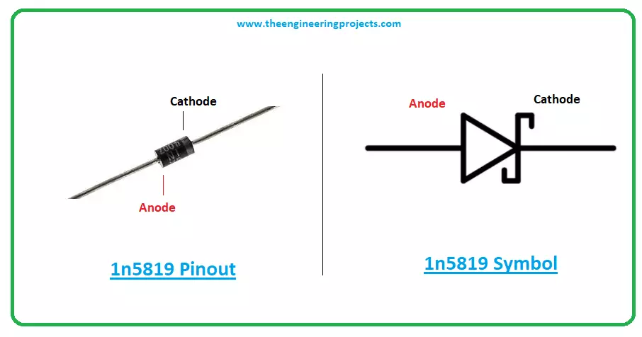
Hello Friends! Happy to see you around. Thank you for clicking this read. In this post today, I’ll document the Introduction to 1n5819. The 1n5819 is a Schottky diode, also called hot-carrier diode, employed for extremely fast switching. This diode is formed when the metal material is combined with the semiconductor material. This combination results in the formation of a barrier that blocks the flow of electrons. The reason this is also called a hot-carrier diode. I suggest you read this post all the way through, as I’ll walk you through the complete introduction to 1n5819 covering datasheet, pinout, features, equivalents, and applications. Let’s get started.

Introduction to 1N5819

  • The 1n5819 is a Schottky diode used for fast switching applications.
  • With high switching speed and low forward drop voltage, this device is employed in high-frequency applications like DC-DC inverters.
  • This diode features low electronic energy in an unbiased condition that is responsible for the creation of a barrier inside the diode that in return blocks the movement of electrons. The formation of a barrier is the reason these Schottky diode devices are also known as a hot-carrier diode.
  • The regular diodes and Schottky diodes are similar devices in terms of the current flow. Both favor the movement of current in one direction only i.e. from the anode terminal to the cathode terminal.
  • These devices are different in terms of the voltage required to power up these devices. Output 2V DC voltage source applied to the diodes, Schottky diodes require only 0.3V, leaving behind 1.7V to power up the diode while regular diode requires only 0.7V leaving behind 1.3V to power up the regular diode.
Know that… where less power dissipation is required these Schottky diodes can be replaced with the MOSFETs.

1N5819 Datasheet

Before working with this component, it’s wise to go through the datasheet of the component that features the main characteristics of the device. You can download the datasheet of this device by clicking the link below.

1N5819 Pinout

The picture below shows the pinout diagram of 1n5819.
  • The component 1n5819 is composed of two terminals. These terminals are used for the external connection with the electrical circuit.
  • One terminal is called anode that is positive while the other terminal is called cathode that is negative.
  • The positive anode is made of metal material while the negative cathode is composed of semiconductor material.
  • The conduction process is carried out from the anode terminal to the cathode terminal. An anode is an area from where current enters the diode and a cathode is the side from where it leaves the diode.

1N5819 Features

The following are the main features of 1n5819 that help you understand how this device is different from its peers available in the market.
  • Diode type = Schottky diode
  • Semiconductor used = n-type
  • RMS Reverse Voltage = 28V
  • Average forward current = 1A
  • Forward Voltage Drop = 600mV at 1A
  • Forward Surge Current = 25A
  • Peak reverse voltage = 40V
  • Available package = DO-41

1n5819 Schottky Diode Construction

  • This Schottky diode is made of metal and semiconductor material. The anode side is composed of metal while the cathode side is made of semiconductor material.
  • The n-type semiconductor is used for the construction of the Schottky diode. The n-type semiconductor is a material where electrons are the majority carriers while the holes are minority carriers. You can also use p-type semiconductor material for the making of this Schottky diode but n-type materials are preferred over p-type material since the latter carries low forward drop voltage.
  • When metals like tungsten, molybdenum, chromium, and platinum are attached with the n-type semiconductor material they constitute Schottky diode.
  • In the Schottky diode, the current moves from the anode terminal to the cathode terminal and this diode blocks the movement of current in the opposite direction.
  • The forward drop voltage on the Schottky diode is mainly related to the nature of metal and the semiconductor material used for the formation of a barrier that restricts the movement of electrons.

1N5819 Applications

The 1n5819 is used in the following applications.
  • Used to control the electronic charge.
  • Used in freewheeling and logic circuits.
  • Used in sample-and-hold circuits.
  • Used in polarity protection and DC/DC converters applications.
  • Used for signal detection and extremely fast switching applications.
  • Used in radio frequency applications and solar systems.
  • Used in high-frequency and low voltage inverters.
That was all about the Introduction to 1n5819. Share your valuable suggestions and feedback around the content we share and help us create quality content based on your requirements. If you have any questions related to this article, you’re most welcome to ask in the comment section below, I’d love to help you the best way I can. Thank you for reading this article.

IRF840 MOSFET Datasheet, Pinout, Features, Equivalent & Applications

Hi Fellas! I hope you’re well today. Happy to see you around. In this post today, I’ll walk you through the Introduction to IRF840.

The IRF840 is an n-channel power MOSFET. It is a fast switching and high voltage device that is available with low on-state resistance. As this is an n-channel MOSFET here conduction process is exercised by the movements of the electrons. In other words, though conduction is carried out by both the movement of holes and electrons, electrons are major carriers in this case.

I suggest you read this entire post till the end as I’ll discuss the complete Introduction to IRF840 covering datasheet, pinout, features, equivalent, and applications. Let’s jump right in.

Introduction to IRF840

  • The IRF840 is an n-channel power MOSFET that supports loads up to 8A and 500V. It is a fast-switching and high-voltage device that requires 10V across the gate terminal to initiate the conduction process.
  • This IRF840 MOSFET is a three-terminal device made of gate (G) drain (D) and source (S) terminals. The external circuits are connected with these MOSFETs through these terminals.

  • This is an N-channel MOSFET, here the conduction process is exercised by the flow of electrons in contrast to the P-channel MOSFET where the conduction process is carried out by the flow of holes.
  • It is important to note that conduction is a process that is carried out inside MOSFET by the movements of both electrons and holes but electrons are major carriers in the n-channel MOSFET devices while holes are major carriers in the p-channel MOSFET devices.
  • The MOSFET stands for Metal Oxide Silicon Field Effect Transistor. It is also known as the IGFET Insulated Gate Field Effect Transistor. It is made by the controlled oxidation of a silicon semiconductor material.
  • MOSFETs and BJTs (bipolar junction transistors) are considered as different semiconductors as BJT is a current-controlled device while the MOSFET is a voltage-controlled device.
  • The voltage applied at the gate terminal usually is directly related to the current between the source and drain terminals. The gate terminal voltage controls the current at the drain and source terminals. Simply put, the gate terminal acts like a control valve that controls the current between two terminals.

IRF840 Datasheet

Before incorporating this device into your electrical project, it’s better to scan through the datasheet of the component that features the main characteristics of the device. You can download the datasheet of this component IRF840 by clicking the link given below.

IRF840 Pinout

The IRF840 is an N-channel power MOSFET. It is a fast-switching device that comes with three pins known as:

  1. Gate
  2. Drain
  3. Source

Recall, the gate terminal controls the current between the source and drain terminals.  The gate terminal initiates the conduction process when we apply the biased voltage of around 10V at the gate terminal.

The following figure shows the pinout diagram of IRF840 MOSFET.

Mind it… generally, the MOSFET is a four-pin component that contains four terminals called:

  1. Source (S)
  2. Gate (G)
  3. Drain (D)
  4. Body (B) / Substrate.

The bodyside is always connected with the source pin. So we generally call the MOSFET a three-terminal device.

IRF840 Features

  • Type: N-Channel fast switching Power MOSFET
  • The rise time and the fall time are 23nS and 20nS respectively
  • Gate threshold voltage (VGS-th) = 10V (limit = ±20V)
  • Continuous Drain Current (ID) = 8A
  • Drain Source Resistance (RDS) = 0.85 Ohms
  • Available package = TO-220
  • Drain to Source Breakdown Voltage = 500V

IRF840 Equivalent

The following are the equivalent of IRF840.

  • 8N50
  • FTK480
  • KF12N50

IRF840 Applications

The IRF840 is used in the following applications.

  • Used in Inverter Circuits and DC-DC Converters.
  • Incorporated in High-Speed switching applications.
  • Used for switching high-power devices.
  • Employed in Control speed of motors and LED dimmers or flashers.

That was all about the Introduction to IRF840. Hope you enjoyed reading this article. If you’re unsure or have any questions, you can pop your query in the section below. I’d love to help you the best way I can. You’re most welcome to share your thoughts about the content we share so we keep sharing quality content based on your needs and requirements. Thank you for reading the article.

1N5818 Schottky Diode Datasheet, Pinout, Features & Applications

Hi Guys! I hope you’re doing well today. I welcome you on board. In this post today, I’ll walk you through the Introduction to 1n5818.

The 1n5818 is a Schottky diode. It is also known as a hot-carrier diode that is employed for extremely fast switching applications. It carries high forward surge capability and low forward drop voltage, making it a suitable pick for high-frequency applications. It is available in the DO-201AD package and comes with very small conduction losses.

I recommend you buckle up as I’ll discuss the complete introduction to 1n5818 covering the datasheet, pinout, features, and applications. Without further ado, let’s get started.

Introduction to 1N5818

  • The 1n5818 is a Schottky diode that is incorporated in extremely fast switching applications. It is also known as a hot-carrier diode.
  • It is available in the DO-201AD package and comes with low forward drop voltage and high forward surge capability.

  • MOSFETs semiconductors are the appropriate alternatives to these Schottky diodes and where less power dissipation is needed, MOSFETs replace these Schottky diodes.
  • Low electronic energy in an unbiased condition is responsible for the formation of a barrier on these Schottky diodes that restricts the movement of electrons. This barrier formation is the main reason these diodes devise are also named hot-carrier diodes.
  • Know that… generally, both the Schottky diode and regular diode are the same devices in terms of the current flow i.e. both devices support the conduction process in one direction only and restrict it in the opposite direction. And current flows from the anode pin to the cathode pin.
  • These devices, however, stand different in terms of the voltage required to power up these devices. Both components receive 2V DC source voltage out of which the Schottky diode requires only 0.3V leaving behind 1.7V to power up the diode devices. And regular diode requires only 0.7V, leaving behind only a 1.3 potential difference to power up the component.

1N5818 Datasheet

Before applying this component to your circuits, it’s wise to read the datasheet that details the main characteristics of the device. Click the link below and download the datasheet of 1n5818.

1N5818 Pinout

  • The following figure shows the pinout diagram of the 1n5818 device.
  • This power diode carries two terminals called an anode and a cathode. The external circuits are connected with the diodes through these terminals.
  • And current flows from the anode terminal to the cathode terminal.
  • The anode terminal is positive while the cathode terminal is negative.
  • The current enters the diodes from the anode pin while it leaves the diode from the cathode pin. Again, the current flows in one direction only.
  • You cannot force this device to flow current in the opposite direction. Doing so will damage the device and thus the entire project.

1n5818 Schottky Diode Construction

  • The 1n5818 is made by the mixture of metal with the semiconductor material which results in the creation of a barrier.
  • When metals like platinum, tungsten, chromium, and molybdenum are joined with the n-type semiconductor material, they create a Schottky diode. The n-type semiconductor is the semiconductor material where electrons work as major carriers and holes work as minority carriers.
  • The Schottky diode comes with two terminals called anode and cathode. The anode side is positive and the cathode pin is negative. The anode pin is made of metal material and the cathode pin is made of semiconductor material. Know that... the current enters the diode from the anode side and it exits the diode from the cathode pin. The current moves from the positive anode side made of metal to the negative cathode side made of semiconductor material.
  • The forward drop voltage of the Schottky diode is mainly dependent on the nature of the metal and semiconductor material that is used to create the barrier that blocks the movement of electrons.
  • Both n-type and p-type semiconductor materials can be employed to operate as a cathode terminal in Schottky diode, but n-type materials are preferred over p-type material because the latter carries with low drop voltage.

1N5818 Features

  • Guarding for overvoltage protection
  • Very small conduction losses
  • Carries high surge capability.
  • Contains low forward drop voltage.
  • Extremely fast switching
  • Available in package DO-201AD.
  • Low forward voltage drop
  • High-frequency operation
  • Protected against overvoltage.

1N5818 Applications

  • Employed in radio frequency applications.
  • Applied in solar systems.
  • Incorporated to control the electronic charge.
  • Used in high-frequency and low-voltage inverters.
  • Used in sample-and-hold circuits.
  • Used for signal detection and extremely fast switching applications.
  • Used in polarity protection and DC/DC converters applications.
  • Used in freewheeling and logic circuits.

That was all about the Introduction to 1n5818. If you’re unsure or have any questions, you can pop your question in the section below, I’d love to help you according to the best of my expertise. You’re most welcome to share your valuable suggestions and feedback around the content we share and keep helping us produce quality content customized to your exact needs and requirements. Thank you for reading the article.

1N4004 Datasheet, Pinout, Features, Equivalents & Applications

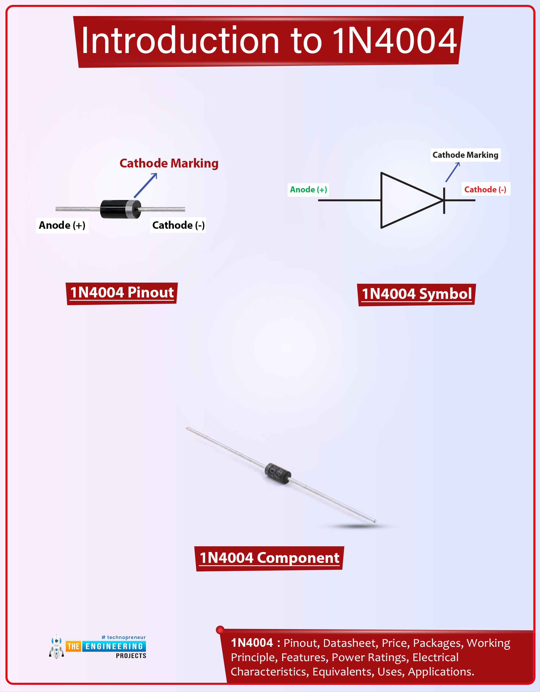
Hi Guys! I welcome you on board. Happy to see you around. In this post today, I’ll walk you through the Introduction to 1n4004.

The 1n4004 is a diode that allows the current to flow in one direction only. It blocks the flow of current in the opposite direction. It comes with two terminals called anode and cathode and current always flows from the anode terminal to the cathode terminal. This device comes with a reverse peak voltage of around 400V and it can support loads under 1A.

I’d recommend reading the Introduction to 1n4007 that I’ve uploaded previously. This diode is almost similar to the device 1n4004 that I’m going to stretch in this post.

I suggest you buckle up as I’ll discuss the complete introduction to 1n4004 covering datasheet, pinout, features, equivalents, and applications. Let’s jump right in.

Introduction to 1N4004

  • The 1n4004 is a diode device that allows the current flow in one direction only. There are terminals on this device that are mainly used for the external connection with the electrical circuits.

  • The grey-colored band on one side represents the cathode terminal. Current always flows from the anode pin to the cathode pin.
  • The 1n4004 is available with a high current capability and low forward drop voltage.
  • Used in current flow regulators, 1n4004 comes in the DO-41 package. And it is a rectifier diode that carries a PN junction. This rectification capability of the device is mainly used to convert AC to DC current.
  • It is employed in general-purpose rectification applications and is electrically compatible with other rectifier diodes.

1N4004 Datasheet

Before applying this device to your electrical project, it’s better to scan through the datasheet of the component that details the main characteristics of the component. Click the link below and download the datasheet of 1n4004.

1N4004 Pinout

The following figure shows the pinout diagram of 1n4004.

 
  • The 1n4004 is a two-terminal device. These terminals are called anode and cathode which carry opposite charges on them. The anode pin is positive while the cathode terminal is negative. The current enters the diode from the anode positive pin and it leaves the diode from the cathode negative pin.
  • The following diagram shows the electrical symbol of 1n4004 where a triangle with a line on one end indicates the presence of a cathode terminal.

And current flows from the anode terminal to the cathode terminal.

1N4004 Features

The features of any device basically demonstrate the specialty of the device based on which this device stands out from the other rectifier diodes available in the market. The following are the main features of the device 1n4004.

  • Non-repetitive Peak  current = 30A
  • RMS reverse voltage = 280V
  • Low forward drop voltage
  • Comes with high current capability
  • Low reverse leakage current = 5uA.
  • Comes in DO-41 Package
  • Average forward current = 1A
  • Peak repetitive reverse voltage = 400V

1N4004 Applications

  • Incorporated as a protection device
  • Used in Half Wave and Full Wave rectifiers
  • Used in Current flow regulators
  • Employed to prevent reverse polarity problem

That’s all for today. I hope you’ve enjoyed reading this article. If you’re unsure or have any questions you can pop your comment in the section below. I’d love to help you the best way I can. Feel free to share your valuable suggestions and feedback about the content we share so we keep sharing quality content customized to your exact requirements. Thank you for reading the article.

TL082 Op-Amp Datasheet, Pinout, Feature & Applications

Hello Guys! I hope you’re well today. Happy to see you around. Thank you for clicking this read. In this post today, I’ll walk you through the Introduction to TL082.

The TL082 is a wide bandwidth dual JFET input operational amplifier. High speed, low cost this device comes with internally trimmed offset voltage. It is available with a fast slew rate, a large gain bandwidth, and a low supply current.

I suggest you buckle up as I’ll discuss the complete Introduction to TL082 covering datasheet, pinout, features, and applications. Let’s get started:

Introduction to TL082

  • The TL082 is a high-speed, low-cost, wide bandwidth and dual JFET input operational amplifier.
  • This component is available with an internally trimmed offset voltage. It comes with a fast slew rate and low supply current.
  • This JFET input device extends low offset and input bias current.
  • The TL082 is electrically compatible with LM1558 and is used to enhance the overall performance of the LM1558 device.
  • With high input impedance and low total harmonic distortion, this device features low noise and offset voltage drift.
  • This amplifier is widely used in audio pre-amplification, sample and hold amplifiers, peak detectors and active filters.

TL082 Datasheet

Before you apply this device to your electrical project, it is better to scan through the datasheet of the device that details the main characteristics of the component. You can download the datasheet of TL082 by clicking the link below.

TL082 Pinout

This device comes with 8 pins as described below.

Absolute Maximum Rating of TL082
Pin No. Rating Symbol
1 Output of op-amp A Output A
2 Inverting Input A Input A
3 Non-inverting Input A Input A
4 Ground V-
5 Inverting Input B Input B
6 Non-inverting Input B Input B
7 Output of op-amp B Output B
8 Voltage supply V+

The following figure shows the pinout diagram of TL082.

Pin 4 is a negative voltage supply or ground while pin 8 is a positive voltage supply.

TL082 Features

The main features of TL082 are mentioned below which will help you understand how this device is different from other operational amplifiers available in the market.

  • Carries Low input bias current = 50 pA
  • Available with Low input noise current = 0.01 pA/Hz
  • Comes with Fast settling time to 0.01% = 2us
  • Contains internally trimmed offset voltage = 15 mV
  • Carries Low input noise voltage = 16nV/vHz
  • Exhibits Low supply current = 3.6 mA
  • Features Low 1/f noise corner = 50 Hz
  • Comes with Wide gain bandwidth = 4 MHz
  • Features High input impedance = 1012?
  • Exhibits High slew rate = 13 V/µs
  • Comes with Low total harmonic distortion = =0.02%

TL082 Applications

TL082 is used in the following applications.

  • Used in function generators and comparators.
  • Used in amplifier circuits.
  • Used in high-speed integrators.
  • Used in other electrical circuits with low input offset voltage.
  • Used in a circuit requiring high input impedance.
  • Used in audio pre-amplification.
  • Used in a sample and hold amplifiers.
  • Used in peak detectors and active filters.

That’s all for today. I hope you find this read useful. If you’re unsure or have any questions, you can pop your comment in the section below, I’d love to help you the best way I can. You’re most welcome to share your valuable suggestions and feedback about the content we share so we keep sharing quality content customized to your exact needs and requirements. Thank you for reading the post.

Syed Zain Nasir

I am Syed Zain Nasir, the founder of <a href=https://www.TheEngineeringProjects.com/>The Engineering Projects</a> (TEP). I am a programmer since 2009 before that I just search things, make small projects and now I am sharing my knowledge through this platform.I also work as a freelancer and did many projects related to programming and electrical circuitry. <a href=https://plus.google.com/+SyedZainNasir/>My Google Profile+</a>

Share
Published by
Syed Zain Nasir