Hey Everyone! Hope you’re well today. I welcome you on board. In this post today, I’ll walk you through the Introduction to Arduino MKR Vidor 4000.
The Arduino MKR Vidor 4000 is a powerful board with which you can develop your own controller board. The inclusion of FPGA makes this device unique and separate from other Arduino boards available in the market. With this FPGA feature, you can do audio and video processing which is not possible with other Arduino boards.
Using this device, you can design a real-time computer reading sensor information and the best part is this board is compatible with all other Arduino boards. With this board, you can make all pins PWM signals (on the FPGA block side) for handling the speed of motors. Moreover, you c ...
Hi Pupils, Welcome to another Experiment of Proteus at The Engineering Projects. Previously, we saw what are the Junction Field Effect Transistors. Today we'll learn about some of the applications of Junction Field Effect Transistors.
Just before the Experiment, it is useful to revise that:
Transistors are three terminal, unipolar Devices. The terminals of Junction Field Effect Transistor are named as :
Drain
Source
Gate
The Gate Terminal is common to both Source and Drain.
Prior to start, let's clear some Concepts about Junction Field Effect Transistor.
Resistor
Resistor is an electrical device. we define the resistors as:
"A Resister is a two terminal Passive electrical device that shows the electrical resistance and is useful in almos ...
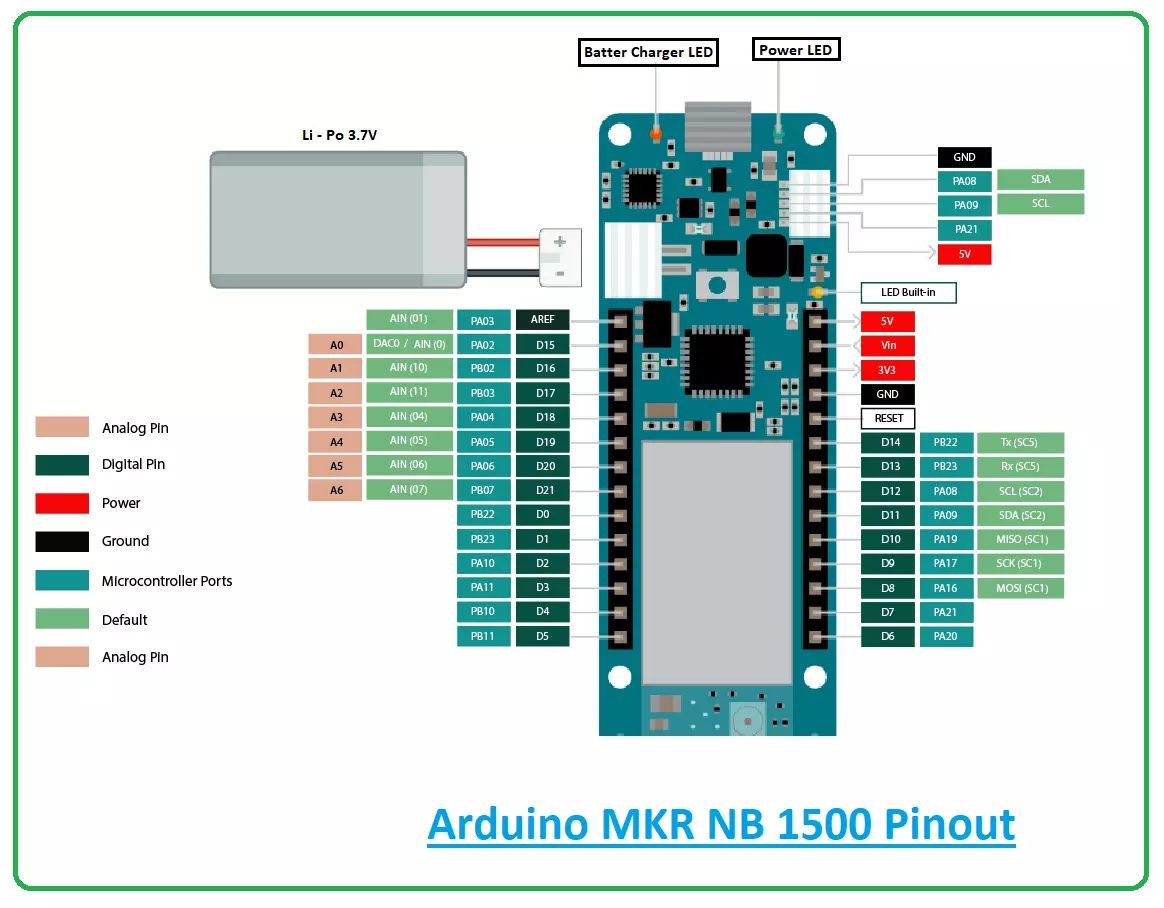
Hi Guys! Hope you’re well today. Happy to see you around. In this post today, I’ll walk you through the Introduction to Arduino MKR NB 1500.
The Arduino MKR NB 1500 is mainly developed for working in remote areas where no power or internet connection is available. This board is based on a SAMD21 Cortex-M0+ 32bit low power microcontroller and comes with an operating voltage of 3.3V.
Admit it.
The Arduino board is a remarkable addition to the development of many automation and embedded projects. These boards are incorporated with a series of digital and analog pins that can be connected with the expansion boards or other breadboards.
Most of the Arduino boards are integrated with 8-bit Atmel AVR microcontrollers. And all these boards incorporate ...
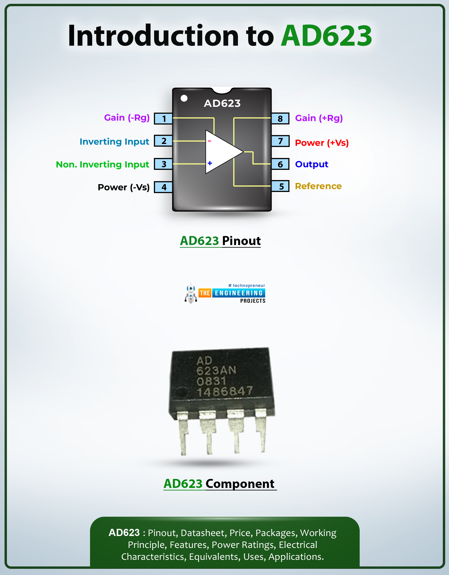
Hi Friends! I welcome you on board. Happy to see you around. In this post today, I’ll walk you through the Introduction to AD623.The AD623 is an instrumentation amplifier integrated with a rail-to-rail feature. It is mainly used in battery-operated applications due to the low current of 500uA.
It features a bandwidth of around 800 kHz which doesn’t require impedance matching since it incorporates buffer amplifiers that are attached to their input pins.
I suggest you buckle up as I’ll detail the complete Introduction to AD623 featuring datasheet, pinout, features, equivalents, and applications.
Let’s jump right in.
Introduction to AD623
The AD623 is an instrumentation amplifier that falls under the category of differential amplifiers that incorporate buffer amplifiers attache ...
Hi Folks! Hope you’re well today. Happy to see you around. In this post today, I’ll walk you through the Introduction to Arduino Pro Micro.
Arduino Pro Micro is an Arduino compatible microcontroller board that is based on ATmega32u4. It operates at a frequency of 16MHz and 5V. It comes with 4 analog pins, 12 digital I/O pins, and 5 PWM pins. Moreover, it also supports serial communication UART with pins Rx and Tx.
Arduino is an open-source platform provided by Arduino.cc that offers both hardware and software customization. Open-source means you can use, edit, or customize the board and software based on your requirements.
Arduino boards are introduced in 2005 in Italy with the aim to provide a single platform where non-tech persons can get a h ...
Hello Everyone! Hope you’re well today. I welcome you on board. In this post today, I’ll walk you through the Introduction to Arduino USB Host Shields.
With Arduino USB host shield you can interface the USB device to your Arduino board. This USB host shield is based on MAX3421E which is mainly known as the USB host controller that contains the analog circuitry and digital logic required to apply the USB full speed peripheral to USB specifications rev. 2.0.
Moreover, this shield is compatible with TinkerKit which projects you can plug this TinkerKit module with the Arduino Boards.
Introduction to Arduino USB Host Shields
Arduino USB host shield is used to connect a USB device with the Arduino Board. Simply put, USB host shields provide the USB ...
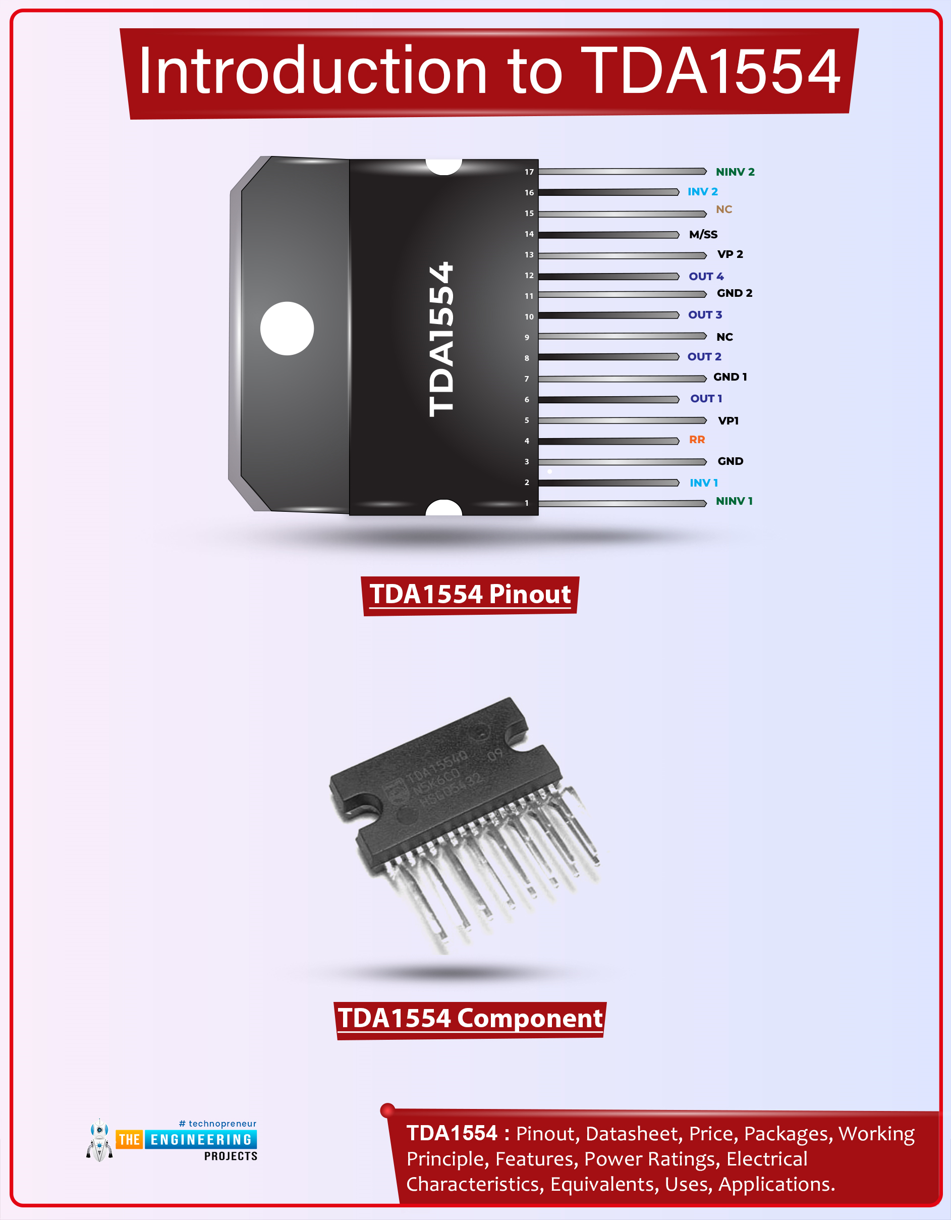
Hi Guys! Hope you’re well today. I welcome you on board. In this post today, I’ll walk you through the Introduction to TDA1554.The TDA1554Q is an integrated class-B output amplifier mainly used for car radio applications. This device features 4 x 11 W single-ended or 2 x 22 W bridge amplifiers. It comes in a 17-lead single-in-line (SIL) plastic power package.
I suggest you buckle up and read this entire post till the end as I’ll discuss the complete Introduction to TDA1554 covering datasheet, pinout, features, and applications.
Let’s get started.
Introduction to TDA1554
TDA1554 is a 4*11W single-ended or 2*22W power amplifier IC which means the internal circuitry features a 4*11W single-ended or 2*22W bridge amplifier.
It is an integrated class-B output amplifier that comes ...
Hi Friends! I welcome you on board. Happy to see you around. In this post today, I’ll walk you through the Introduction to Arduino Pico.
Arduino Pico is the world’s smallest Arduino compatible board, as said by Arduino Official Page. Because of its small size & low weight, it is normally used in autonomous projects i.e. drones, robots, quadcopters etc. where size is the real issue.
Arduino boards are introduced in modern electronics, to make projects economical and easy to design. A common man with no prior knowledge about programming can get hands-on experience with them. This smallest Pico version is readily available to turn your innovative thoughts into reality.
I suggest you read this post all the way through as I’ll detail the complete I ...
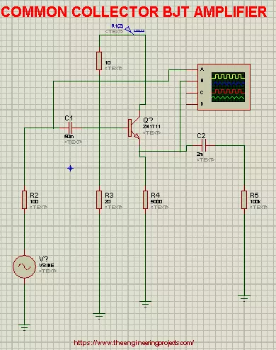
Hi Mentees, Welcome to a new tutorial at The Engineering Projects. Today You will unearth about Common Collector bipolar Junction Transistor Amplifiers. Before this, we learnt about two types of Configurations of Transistors named Common Emitter BJT Amplifiers and Common Base BJT Amplifiers.
In this tutorial We'll discuss about:
Introduction of Common Collector BJT Amplifier.
Basic Concepts for the Common Collector BJT Amplifiers.
Implementation of Common Collector BJT Amplifiers in Proteus ISIS.
Characteristics and advantages of Common Collector BJT Amplifiers.
So that, you can get the best understanding about the topic and its practical implementation.
Introduction
1st of all, We'll have a brief definition of the Common Collector Ampl ...
Hi Everyone! Hope you’re well today. Happy to see you around. In this post today, I’ll walk you through the Introduction to TDA2005.TDA2005 is a 20-watt Class B dual audio amplifier integrated chip. It comes in a Multiwatt11 package and is carefully designed for car radio applications. It can support the current up to 3.5A which is quite high which makes it a suitable pick for constructing power booster amplifiers.
I suggest you read this post all the way through as I’ll detail the complete Introduction to TDA2005 covering datasheet, pinout, features, and applications.
Let’s jump right in.
Introduction to TDA2005
TDA2005 is a 20-watt Class B dual audio amplifier integrated chip. It is particularly designed for car radio applications.
...