Hello Learners! welcome from the team of The Engineering Projects. We hope you are having a productive day. We are working on a series of Blogs based upon the core knowledge about Digital Logic Gates and Circuits. In this tutorial, we'll know about the SR Flip Flops and after brief introduction we will simulate SR Flip Flops in Proteus. Let's have a glimpse on the topics of today:
What are Flip Flops?
What are the types of Flip Flop?
How does we design the Truth Table of SR Flip Flops?
What are further classes of SR Flip Flips?
Implementation of SR Flip Flops in Proteus.
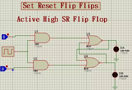
Flip Flops
Flip Flops are extremely important Circuits of Digital Logic Design. We Introduce the Flip Flops as:
"Flip Flops are type of sequential Logic Circuit that co ...
Hello Everyone! Hope you’re well today. Happy to see you around. In this post today, I’ll walk you through the Introduction to Arduino Uno WiFi Rev 2.
Arduino Uno WiFi Rev 2 is a microcontroller board based on ATmega4809 and carries an ECC608 crypto chip to ensure a secure and safe WiFi connection. The board contains 14 digital I/O pins, 5 PWM pins, 6 analog pins, one SPI protocol, one I2C, and one UART communication protocol.
I suggest you read this entire post till the end as I’ll detail the complete Introduction to Arduino Uno WiFi Rev2 covering pinout, pin description, features, programming, and applications.
Let’s jump right in.
Introduction to Arduino Uno WiFi Rev 2
The Arduino Uno WiFi Rev 2 is a microcontroller board that is mainly ...
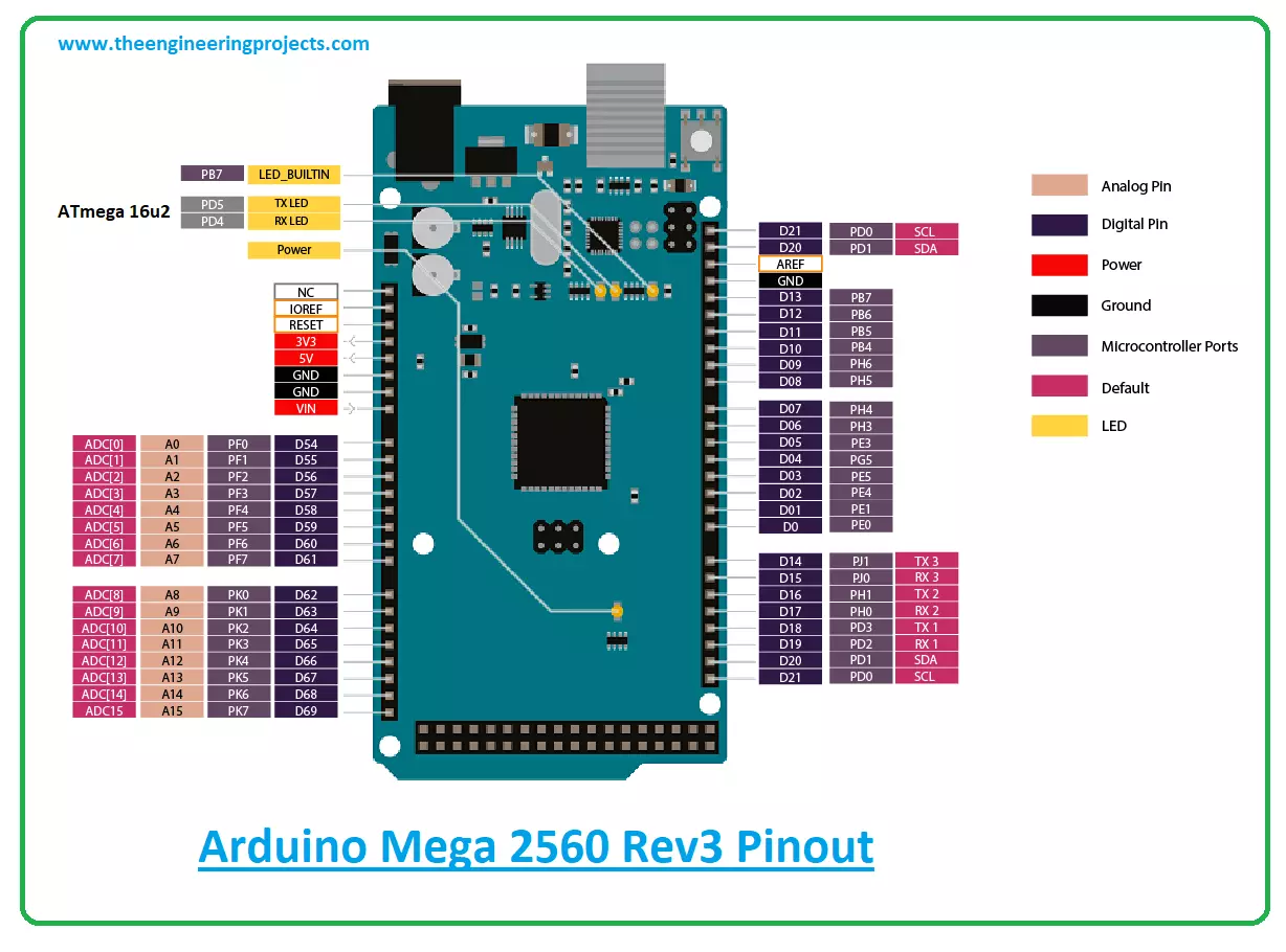
Hi Friends! Hope you’re well today. In this post today, I’ll walk you through the detailed Introduction to Arduino Mega 2560 Rev3.The Arduino Mega 2560 Rev3 is a microcontroller board that is based on the ATmega2560 microcontroller.
The Arduino boards are widely used in the automation industry and embedded projects. Other boards like Arduino Uno, Arduino Nano, Arduino Every, Arduino Beetle all seem a good pick for the projects that require little memory to store the program. However, when the nature of projects becomes complex, requiring more memory and a rich set of I/O interfaces, the Arduino Mega 2560 Rev3 comes into play. In order to power up these Arduino boards, we need to use a Power supply for electronics or we can also use the USB port on ...
Hello Learners, hope you are doing well. I am here with a new tutorial. We'll discuss about Junction Field Effect transistors. In this tutorial, we will learn the basic Introduction to JFET nad will also have a look at its practical Implementation and simulation in Proteus.
Basically, Junction Field Effect is a type of transistor, similar to Bipolar Junction Transistors but they have different characteristics due to some reasons as discussed below:
Introduction to JFET
We Define the JFET as:
"Junction Field Effect transistors or simply JFET is the semiconductor ,Voltage Control, three terminal device that is present in both configurations either N channel or P channel."
JFET are named so because the the operation of JFET relies on the Field of th ...
Hi Guys! Hope you’re well today. Happy to see you around. In this post today, I’ll walk you through the Introduction to Arduino Nano 33 IoT.
Arduino Nano 33 IoT is mainly used in basic IoT applications. The Internet of things is one of the most exciting and robust developments in the field of information technology.
Using this technology you can interface a network of physical things with software, sensors, or other technologies to develop communication and data exchange between devices and other systems using the internet.
For example, you can control the room temperature by interfacing the sensors in your rooms with your smartphone through WiFi. Traditional systems including control systems, wireless sensor networks, embedded systems, and hom ...
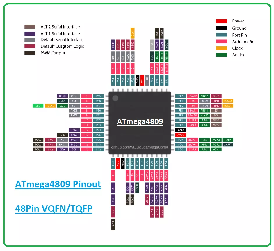
Hi Guys! I welcome you on board. Happy to see you around. In this post today, I’ll walk you through the Introduction to ATmega4809.
The ATmega4809 is a type of microcontroller that belongs to the megaAVR® 0-series. It features an AVR® processor with a clock speed running at up to 20 MHz. It comes with a Flash memory size up to 48 KB, 256 bytes of EEPROM, and 6 KB of SRAM. It is available in 28-, 32-, 40-, or 48-pin packages.
I suggest you buckle up as I’ll detail the complete Introduction to ATmega4809 covering datasheet, pinout, features, power ratings, and applications.
Let’s get started.
Introduction to ATmega4809
The ATmega4809 microcontroller belongs to the megaAVR® 0-series that contains an AVR processor.
The series carries low power ...
Hi Guys! Hope you’re well today. I welcome you on board. In this post today, I’ll walk you through the Introduction to Arduino Nano 33 BLE.
Arduino Nano 33 BLE is an advanced version of Arduino Nano board that is based on a robust and powerful processor the nRF52840 from Nordic Semiconductors, a 32-bit ARM® Cortex™-M4 CPU. It comes with a crystal oscillator frequency of around 64MHz. It features 32 times bigger program memory than the Arduino Uno board, helping you store programs with much larger memory. With this device, you can produce a lot more variable as it comes with RAM that is 128 times bigger than the RAM of Arduino Uno.
Before you move further, I recommend you read this article on the Introduction to Arduino Nano which we have publish ...
Hi Guys! I welcome you on board. Happy to see you around. In this post today, I’ll give you a detailed Introduction to Arduino MKR WiFi 1010.
The Arduino MKR Wifi 1010 is a solution to your basic IoT applications. Using this device, you can develop a WiFi-connected sensors network or can produce a BLE device connected to your cell phone. This board is based on the SAMD21 microcontroller and comes with a clock speed of around 32.768 kHz (RTC), 48 MHz. There are 8 digital pins, 13 PWM pins, and 7 analog pins incorporated on the board. The operating voltage is 3.3V while the voltage through USB or Vin is 5V.
I suggest you read this post all the way through, as I’ll detail the complete introduction to Arduino MKR Wifi 1010 covering pinout, pin descr ...
Hi Guys! Hope you’re well today. I welcome you on board. In this post today, I’ll walk you through the Introduction to Arduino MKR WAN 1310.
The Arduino MKR WAN 1310 includes Lora connectivity that can perform very long-range transmission operations consuming low power.
This device is an ideal pick for the hobbyists requiring to develop IoT devices using the minimum networking experience using low power devices.
The MKR WAN 1300 is incorporated with the Microchip® SAMD21 which is the low-power processor, the MKR family’s characteristic crypto chip (the ECC508), and the Murata CMWX1ZZABZ LoRa® module.
Before you read further, I recommend you have a look at Introduction to Arduino Nano Every and Arduino MKR Vidor 4000 that I have uploaded previo ...
Hi Guys! I welcome you on board. Thank you for clicking this read. In this post today, I’ll detail the Introduction to Arduino Nano Every.
Arduino Nano Every is a tiny powerful board that is based on the ATMega4809 AVR processor. It comes with a clock speed of around 20MHz and flash memory of around 48KB. It carries two 15 pin connectors on each side of the board that are pin-pin compatible with the Arduino Nano Every.
The low price and small size make this board an ideal pick for the range of electrical projects like electronic musical instruments, low-cost robots, and general development of the small parts of the large projects.
Needless to say, Arduino has been a cornerstone of many electronic projects ranging from simple student projects to ...