Hello everyone! I hope you all will be absolutely fine and having fun. Today, I am going to elaborate about the Introduction to LM324. It is an Operational Amplifier (Op-amp) consists of four channels. Its a low cost device having true differential inputs.For single supply applications LM 324 are superior to the other operational amplifiers. LM-324 is capable of operating at the minimum voltage up to 3V and at the high voltage levels up to 32V.
One of the major advantage of LM-324 is that common mode input range includes negative supply which eliminates the need of external biasing. Negative power supply voltage is also included in output voltage range. This device is lead (Pb) free, halogen free and RoHS compliant. It consists of four amplifier ...
Hello everyone I hope you all will be absolutely fine and having fun. Today, I am going to share my knowledge on Introduction to TL494. It supports all of the functions that are necessary for the Pulse Width Modulation (PWM) control circuits. Power supply control is the basic purpose of the TL494 device. It has an output control circuit, a flipflop, dead time comparator, two different error amplifiers, 5V reference voltage, oscillator and a PWM comparator. TL 494 operates properly between the frequency of 1kHz to 300kHz.
The Dead Time Comparator (DTC) provides around 5% of dead time. Both of the error amplifiers display a common-mode voltage from -0.3V to (Vcc-2)V. If we provide a sawtooth wave at the CT terminal and terminate RT to the referenc ...
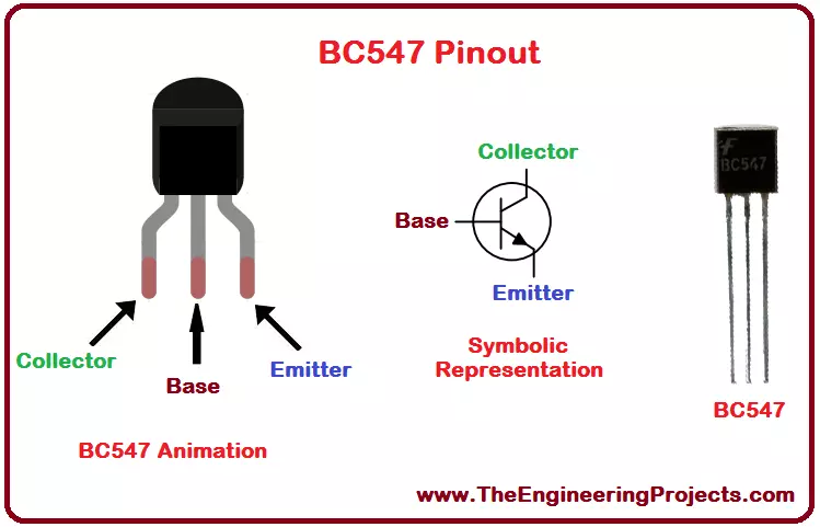
Hello everyone! I hope you all will be absolutely fine and having fun. Today, I am going to give you a detailed Introduction to BC547. It is an NPN bipolar junction transistor (BJT), mainly used for switching and current amplification.
Its maximum current gain is around 800. So, let's have a detailed overview of BC 547.
Introduction to BC547
BC547 is a 3-Terminal NPN Bipolar Junction Transistor(BJT), mostly used for switching purposes and current amplification.
BC547 Pins(Terminals) from left to right are called:
Collector.
Base.
Emitter.
Depending on the voltage applied at Base Terminal, BC547 can operate in two states, named:
Forward Biased.
Reverse Biased.
BC547 as Reverse Bias ...
Hello everyone! I hope you all will be absolutely fine and having fun. Today, I am going to give you an Introduction to LM741. It belongs to the series of general purpose amplifiers. It supports larger range of input voltages. LM741 provides high gain and short circuit protection as well. Its pins configuration is very similar to UA709 and there is no need of frequency compression in LM 741.
LM741 can be used as a comparator in order to determine the levels of applied input voltages i.e. either smaller or larger input voltages are applied at its input terminal. LM741 is an op-amp IC having 8 different pins, which will be explained later in this tutorial. LM-741 has a very wide range of applications e.g. function generator, comparator, DC amplifie ...
Hello everyone! I hope you all will be absolutely fine and having fun. Today, I am going to share my knowledge with all of guys about Introduction to IRF540. It is basically an N-Channel power Metal Oxide Silicon Field Effect Transistor (MOSFET) and operates in enhancement mode.
MOSFET is a lot sensitive in comparison to an FET (Field Effect Transistor) due to its very high input impdence. IRF540 can perform very fast switching as compared to the normal transistor. It is based on HEXFET technology and operates on the temperature ranging from -55 degrees celsius to 175 degree celsius. If we need some switching application between different signals or to perform any of amplification process, MOSFET IRF540 will be the best option in this case bec ...
Hello everyone! I hope you all will be absolutely fine and having fun. Today, I am going to explore my knowledge about Introduction to LM317. It is basically a positive voltage regulator having three terminals. It can a supply a current more than 1.5A and voltage in a range of 1.25V to around 37V. You should also have a look at this LM 317 Calculator.
For the adjustment of output voltage only two external resistors are required. It has improved standards of line regulation as well as load regulation. Full overload protection e.g. current limiting, area protection can be achieved using LM317. If its adjusting terminal is disconnected, even then all of the protection circuits will work properly. We can also use LM317 as precision current regulator ...
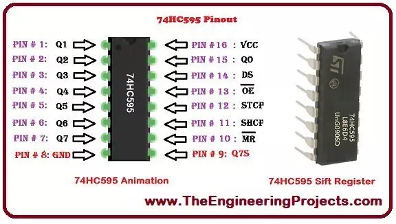
Hello everyone! I hope you will be absolutely fine and having fun. Today, I am going to explain all of you about Introduction to 74HC595. It is basically a shift register. It has an ability to store and to shift the data of 8 bits. First of all the data is written on the register serially and then it goes to the storage register. All of the output lines are controlled by this register.
74HC595 register is a very high speed device based on Complementary Metal Oxide Semiconductor (CMOS). 8 bit data register receives the data from the input DS. This data is then transferred from the input shift register to the output shift register. 74HC595 has a vey wide range of applications in daily life. It can be used as serial to parallel data converter, can ...
Hello everyone! I hope you will be absolutely fine and having fun. Today, I am going to give an Introduction to 2N3904. It is basically an NPN transistor made up of silicon material. It acts as a general purpose amplifier and switch. You should also have a look at Introduction to 2N2222, which is also an NPN transistor and considered as 2N3904 equivalent.
It is mostly used for lower power amplifiers and switching applications. Its major functional area is enclosed in TO-92 package. Its a silicon NPN general purpose bipolar junction (BJT) transistor designed for switching purpose as well as for an amplifier. Its can bear lower amount of current, lower power and medium voltage levels. It is most commonly used BJT due to its smaller size, wide avai ...
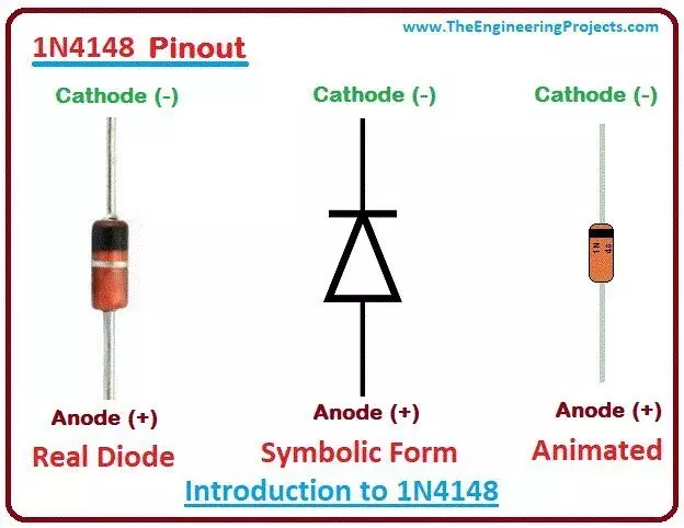
Hello everyone! I hope you will be absolutely fine and having fun. Today, I am going to give an Introduction to 1N4148. It is basically a diode used for fast switching purposes. Switching diodes are usually single P-N diodes and their functionality is similar to that of normal switch.
Below a specific voltage, switching diodes i.e. 1N4148 has high resistance. Whereas as above that specific voltage they show a low resistance. It is a most commonly used diode due to its smaller size, easy availability and low cost. Good switching diode can be chosen by its maximum reverse recovery time and its power dissipation ranging from 80mW to 1kW. Switching diodes such as 1N4148, 1N4007 etc. have very wide range of applications specially in Embedded Systems ...
Hello everyone! I hope you will be absolutely fine and having fun. Today, I am going to give you an Introduction to 2N2222. It is the most commonly used Negative-Positive-Negative (NPN) Bipolar Junction Transistor (BJT) available in the market now a days. 2N2222 can be used for different purposes e.g. switching and amplification of analog signals. I hope you have enjoyed the previous post on Introduction to ULN2003.
The major functional area of 2N2222 is enclosed in TO-18 package. Due to the low cost and small size it is the most commonly used transistor. One of its key features is its ability to handle the high values of currents as compared to the other similar small transistors. Normally it is capable of switching a load current of 800mA whic ...