Introduction to JFET
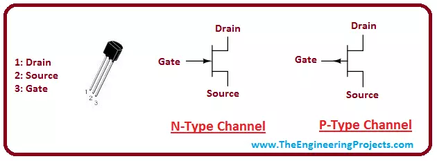
Hello Guys! I hope you are doing great and having fun. I am back to give you a daily dose of knowledge that will enhance your learning skills and put you ahead of others. Today, I am going to give you details on the
Introduction to JFET. It is a Junction Field Effect Transistor that consists of three terminals named drain, source and gate. It comes in two configurations called the P-Type channel and the N-Type channel. I'll give you brief details on JFET and try to cover as many aspects as possible. Let's get started:
Introduction to JFET
- JFET (Junction Field Effect Transistor) is a uni-polar voltage-controlled device that consists of three terminals called drain, source and gate.
- Unlike bipolar junction transistors which are bipolar current-controlled devices in which a small amount of base current is used to control a large amount of current at the collector and emitter side, JFET is a uni-polar voltage-controlled device in which voltage applied to the gate terminal allows the current to flow through JFET, resulting in input applied voltage equals to the current flowing through the transistor.
- In JFET, gate is always negatively biased as compared to source.
- As compared to bipolar junction transistors, JFET are uni-polar because current carriers in case of JFET are either electrons or holes while bipolar junction transistors are operated by the movement of both electrons and holes.
- The operation of JFET depends on the electric field created by input applied voltage, hence it is called Field Effect Transistor.
- JFET can be classified into two types on the bases of their operation i.e. N-Type and P-Type JFET.
- In JFET, current carrying path between drain and source is called channel which contains no pn-junction. Channel can be made up of P-Type or N-Type semiconductor.
- Current flowing through this channel widely depends on the input voltage applied to the gate terminal of JFET.
- Field effect transistors generally comes in two types JFET (Junction Field Effect Transistors) and MOSFET( Metal Oxide Semiconductor Field Effect Transistors)
- As stated earlier, JFET contains no pn-junction, instead it comes with channel that consists of N type or P type semiconductor that passes between source and drain terminals of JFET.
JFETs are classified into two main configurations.
- N-Type Configuration
- P-Type Configuration
1: N-Type Configuration
- In N-Type configuration current flowing through the channel is negative i.e. current flow is carried out by the flow of electrons which are also termed as donor impurities.
- The measure of conductivity of electron in N-Type configuration is much higher than the holes in P-Type configuration, because electrons come with high level of mobility than holes. Hence, in terms of conductivity, N-Type configuration is more efficient than P-Type configuration.
- Channel is a conducting path between drain and source. Within this channel, there lies a third terminal called Gate at which input voltage is applied that is used to control the current flowing through the JFET.
- As channel is resistive in nature, resulting in creating the voltage gradient which becomes less positive as we move from drain to source terminal. This less positive voltage makes drain terminal high reverse biased and source terminal low reverse biased. This bias creates a depletion region whose width is directly proportional to the bias itself.
- The current carrying path between source and drain is controlled by the voltage applied to the gate terminal. In an N-Type configuration of JFET this gate voltage is negative while in case of P-Type configuration it is positive.
- It is important to note that gate current in reverse biased condition in the JEFT is practically zero, while base current in Bipolar junction transistor always comes with a value greater than zero.
N-Type Channel Biasing
- Following is the figure shows N-Type semiconductor with P-Type material which forms the reverse biased PN-junction that creates a depletion region around the gate terminal of JFET.
- Depletion region will be created in the absence of external voltages. JFET are also termed as depletion mode components.
- The depletion region will create a voltage gradient of some thickness which ultimately limits the flow of current, hence results in increasing the overall resistance of FET.
- It is clear from the figure above that most part of depletion region lies between the gate and drain terminals which least part lies between the gate and source terminals which means resistance between gate and drain terminal appears more than the resistance between gate and source terminals.
- In the absence of external input voltage at gate and small voltage at the drain and source Vds allows the saturation current to flow between drain and source.
- The amount of current flowing through the pn-junction will be restricted by the depletion region around the pn-junction.
- It is important to note, if we apply negative voltage at the gate and source Vgs terminals, it will cause the depletion region to grow which ultimately restricts the flow of current, hence results in decreasing the overall conduction of transistor.
- If the voltage applied at the gate terminal Vgs appears to be more negative, it will allow the depletion region to increase and results in decreasing the overall width of channel. The moment comes when applied voltage at gate terminal appears to be negative to the point that will squeeze the channel and won't allow a fraction of current to flow between source and drain terminals.
- The negative voltage applied to the gate terminal at which no current flows between drain and source terminals is called "Pinch-off Voltage".
- In pinch off region negative voltage at the gate terminal Vgs controls the overall conductivity of the channel. This is the reason JFET are called voltage controlled devices.
- Voltage appears at the gate terminal must not be positive, otherwise it will make resistance zero and allows the current to flow between gate terminal instead of source terminal. Positive voltage at the base terminal can damage the transistor at large.
2: P-Type Configuration:
- In P-Type configuration current flowing through the channel is positive i.e. current flow is carried out by the flow of holes which are also termed as acceptor impurities. Both N-Type and P-Type configurations come with same characteristics with some exceptions.
- Current carriers in N-Type configuration are electorn, hence current appears to be negative
- Current carriers in P-Type configuration are holes, hence current appears to be positive.
- Biasing voltage in P-Type configuration comes with reverse polarity.
- The voltage applied at the gate terminal is used to control the current flowing between source and drain. As JFET is a voltage controlled device and no current flows through gate terminals Ig=0. Hence in that case, current flowing out from source terminal will be equal to the current flowing into the drain terminal i.e. Is=Id
V * I Curves of N-Channel JFET
Following figure depicts the four region of operation of JFET.
- Ohmic Region: Region is called ohmic region when Vgs=0. In this region JFET operates like a voltage controlled resistor.
- Pinch off or Cut-off Region: It is region at which voltage applied to the gate is negative to the point which causes depletion region to increase and allows the current carrying width to decrease till it disappears, resulting in maximum resistance to appear and current flowing through the channel will be zero.
- Active or Saturation Region: The region that is controlled by gate voltage Vgs and where JFET becomes good conductor is called active region. Vds has no effect on active region.
- Breakdown Region: Region is termed as breakdown region where voltage between source and drain appears to be maximum to the point where it breaks the resistive channel and allows the current to flow between the channel.
V * I Curves for P-Type JFET
- The curves for P-Type configuration appear to be same with one exception i.e. Increase in positive voltage at the gate terminal will decrease the current at the Drain terminal Id.
Formula for Drain Current and Drain-Source Channel Resistance
- Drain current at the saturation region can be calculated as follows:
Id= Idss * [ 1 - Vgs / Vp ]
- Id lies between zero to Idss.
- Similarly, if we know drain source voltage Vds and drain current Id, we can calculate the drain-source channel resistance.
Rds = ?Vds / ? I d = 1 / gm
- Here gm represents the "transconductance gain"
Different Modes of Operation of FETs:
FETs can be classified into three different modes of configuration.
- Common Source Configuration
- Common Gate Configuration
- Common Drain Configuration
1: Common Source Configuration CS:
Common source configuration is an analogous to the common emitter configuration in the bipolar junction transistors. In this configuration input voltage is applied to the gate terminal and output we get is from the drain terminal. This mode of operation comes with amplified voltage and high impedance, hence it is mostly used in high audio frequency amplifies. As this is an amplifying circuit, it allows the output to be diverted 180º from its input.
2: Common Gate Configuration CG:
Common gate configuration is an analogous to the common base configuration in the bipolar junction transistors. In this configuration input voltage is applied to the source terminal and output appears at the drain terminal while gate is connected to ground. In this configuration impedance will be low as compared to common source configuration. This configuration is mostly used in high frequency and impedance matching circuits. Unlike common source configuration, here "output signal is in phase with the input signal"
3: Common Drain Configuration CD:
Common drain configuration is an analogous to the common collector configuration in the bipolar junction transistors. In this configuration input voltage is applied to the gate and output signal is collected from the source. It is important to note there is no signal applied to the drain terminal. Vdd simply depicts the bias voltage. Similar to common gate configuration, here "output signal is in phase with the input signal"
Comparison between BJT and JFET
-
- Both, bipolar junction transistors and uni-polar field effect transistors encompass same characteristics with some exceptions.
- BJT are bipolar devices i.e. they are operated by the movement of both electrons and holes. JFET are unipolar devices i.e. they are operated by the movement of either electrons or holes.
- As compared to Bipolar junction transistors, JFET comes in much smaller form and can be used in many tiny electronic chips.
- One major feature that differentiates between bipolar junction transistors and JFET is the input impedence. It is very high in case of JFET while it appears very low in bipolar junction transistors.
Applications
- JFET are widely used in many electronic appliations. They are mainly used for amplification purpose.
- JFET are used to obtain high frequency audio signal.
- They are useful for obtaining impedance matching circuits.
That's all for today. I hope you have got a clear idea about JFET. However, if still you feel any doubt or query in understanding the concept of JFET, you can ask me in the comment section below. I'll be glad to help you in this regard. Your feedback and suggestion will be highly appreciated. It will help us give you quality work that resonates with your needs and expectations. Stay tuned!
Introduction to BF259
Hello Friends! I am back again to fill your appetite with more knowledge and skills. Today, I am going to explain the details on the
Introduction to BF259. It is a bipolar NPN (negative-positive-negative) silicon transistors which comes in metal casing. It consists of one P layer that lies between the two layers of N doped semiconductor. I am going to cover all aspects related to this bipolar transistor. Let's get started and have a look, how it works and what are the applications it finds useful.
Introduction to BF259
- BF259 is a bipolar silicon transistor which is made up of two N doped layer and one P doped layer.
- It is mainly a three terminal device which consists of emitter base and collector.
- P terminal of the transistor acts like a base while other two sides of P layers act as emitter and collector respectively.
- Small current at the base is used to control a large amount of current at the collector and emitter side.
- The power it can dissipate is 1 W, while transition frequency is about 75 MHZ.
- DC collector current is 100mA.
- Maximum power dissipation across collector is 0.5 W.
- BF259 is also considered as a current operated device.
- Maximum collector base voltage is 300 V and is denoted by Vcb.
- Maximum collector emitter voltage is 300 V and is denoted by Vce.
- It comes with lots of major applications but mainly it is used for switching and amplification purpose.
1. BF259 Pinout
BF259 NPN silicon transistor consists of three terminals.
1: Emitter
2: Base
3: Collector
Actual pinout of this NPN transistor is given in the figure below
- The base current is used to control the large amount of current on the collector and emitter side.
- The way the base current impact the emitter and collector current is used for the amplification applications.
- This bipolar transistor will turn ON when current flows from emitter and collector.
2. Mechanical Outline of BF259
The mechanical outline of bipolar silicon transistor BF259 is shown in the figure below:
- All the dimension are given in mm.
- You must take these dimension into consideration before you plan to make a circuit so these dimension properly fit in the circuit.
3. Circuit Diagram of BF259
The circuit symbol of BF259 is shown in the figure below:
- This NPN silicon transistor comes with a positive base side and negative emitter side.
- Emitter current is the sum of base and collector current.
- Small amount of current at the base side is used to handle the large amount of current at the emitter and collector side.
- Main difference between NPN and PNP transistor is, Current will sink into the base side in case of PNP transistor while current from the base side will source to the transistor in case of NPN transistor.
- Transistor current can be found by dividing the collector current to the base current. It is also called beta current and is denoted by ß. Beta has no units as it is a ratio between two currents.
- Value of beta is used for the amplification purpose. Beta value ranges between 20 to 1000, however, its standard value is 200.
- The ratio between collector current to the emitter current is called current gain of the transistor and is denoted by alpha a.
- The value of alpha ranges between 0.95 to 0.99, however, in most of the cases it is considered as 1.
4. Absolute Maximum Rating BF259
The maximum absolute rating of BF259 is shown in the figure below.
- Units of current and voltage are mA and V receptively.
- These rating are important for many engineering projects.
5. Applications
- BF259 is also called high voltage video amplifier and is mostly used for high voltage video output.
- It is also used for the audio output stages.
- These transistors are the main drivers for horizontal deflection circuits.
That's all for today. If you have any question you can easily ask in the comment section below. I'll try my best to help you solve your queries. Your suggestion and feedback will be highly appreciated. Stay tuned for next article.
Introduction to 2n4402
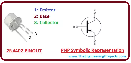
Hey guys! I aspire you a prosperous life filled with joy and happiness. Today, I am going to uncover the details on the
Introduction to 2n4402. It is basically a PNP (Positive-Negative-Positive) silicon transistor where N doped layer lies between the two P doped layer. It consists of three terminals i.e. emitter, base, collector. Here N represents the base of the transistor and two P layers represents the emitter and collector respectively. I'm going to cover all aspects related to this transistor. Let's hop on the board and dive in the details of this silicon transistor.
Introduction to 2n4402
- 2n4402 is a bipolar silicon transistor, where one layer of N doped semiconductor is sand-witched between the two layers of P doped semiconductor.
- It works in a way, the small current at the end of the base is used to control a large amount of current at the end of collector and emitter.
- PNP transistor works in a similar way to NPN transistor with the exception of current carriers. In case of NPN transistors, current carriers are electron while current carriers in the case of PNP transistors are holes and direction of current and polarities of voltage will be reversed in this case.
- In PNP transistor, P letter represents the polarity of voltage applied to the emitter which is positive and N letter shows the polarity of voltage applied to the base which is negative. In order to conduct in PNP transistor, Emitter will always be more positive than base and collector.
2n4402 Pinout
2n4402 consists of three pins
- 1: Emitter
- 2: Base
- 3: Collector
- Unlike NPN transistors, here current flows from emitter to collector and current carriers are holes.
PNP Circuit Symbol
- Following is the circuit symbol of PNP transistor. It consists of two P layers and one N layer.
- The polarity at the emitter side is positive with respect to both base and collector.
- The base of this transistor is negative with respect to emitter.
- Current flowing through the emitter side is the sum of current flowing through collector and base.
- Small amount of current at the base side is used to control the large amount of current at the collector and emitter side.
- PNP and NPN works in similar way with the exception of current direction and medium used for the flow of current.
- In PNP transistor current flows from emitter to collector and current carriers in this case are holes which are collected by the collector.
PNP Transistor Configuration
- Transistor configuration of PNP 2n4402 transistor is shown in the figure below:
- Emitter is positive with respect to collector and base
- Small amount of base current is used to control the large current at the collector and emitter side.
- Current carriers are holes which are collected by the collector.
Transistors as a Matched Switch
- In most of the cases, PNP transistors replace the NPN transistor with the only exception in the direction of current and polarities of voltages.
- Like NPN transistor, PNP transistor can also be used as a switching device.
- You might think what is the point of using PNP transistor while there are lots of NPN transistors out there that can be used as a switch or for amplification purpose. However, taking two types of transistors come with a lot of advantage in designing the power amplifier circuit.
- Class B-amplifiers come with a two pair of NPN and PNP transistor, where both transistors are used to control the current flowing in both directions at any instant of time. Transistors are called "Complementary Transistors" which use both NPN and PNP transistor of identical characteristics.
- In Class B-amplifiers, both transistors work in a similar way i.e. NPN transistors conducts for the positive half cycle and PNP transistor conducts for the negative half cycle of the transistor. This results in flowing the power at the load out put in both directions. PNP transistors will switch on when it sinks current to its base side and it will switch off when current at the base side stops to flow.
Applications of 2n4402
- These transistors are mainly used for voltage and power amplification.
- In combination with NPN transisters, these PNP transistors form a perfect bond through which current flows alternately from both sides of NPN and PNP transistors.
That's all for today. I hope you'd enjoyed our article. If you have any query or question you can easily ask in the comment section below. I'd be glad to help you in this regard. Your suggestion and feedback will be highly appreciated. Stay tuned for next article.
Introduction to Resistors
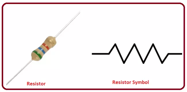
Hey guys! I hope you are doing good and having fun. Today, I am going to unlock the details on the
Introduction to Resistors. Resistor is a two terminal component that is used to restrict the flow of current. Resistors are widely used in electrical circuits. They come in different forms ranging from variable resistors to fixed resistors. Depending on the feature of resistors, both are used in many applications. I am going to cover all aspects relating to resistors. Let's get started.
Introduction to Resistors
- A resistor is a two-terminal device that is used to resist the flow of current. It is one of the most commonly used components in electrical circuits.
- Resistance of any resister is described in ohms. Ohm is denoted by the Greek letter omega. Each resister has a different value of resistance which tells us how strongly it resists the flow of current. More the value of resistance more is the capability of resisting the current.
- Resistance will be considered as one ohm if the potential difference between the two ends of the conductor is 1 V and a current flowing through it is 1 Ampere.
- Resistance can be derived from Ohm's law which indicates voltage is directly proportional to the current flowing through the conductor.
V= I * R
- Each resistor comes with two wires, also called as leads. Between these two leads there lies a ceramic part which actually resists the flow of current. Resistor consists of three colored strips that indicate the value of resistance.
- Some resistors come with four colored strips. In such case, fourth strip indicates the value of tolerance. Tolerance is the value of the deviation of resistance from its given value on the resistor. Gold color of forth strip indicates tolerance is 5% and silver color indicates tolerance is 10%. Where there is no forth strip, tolerance is considered as 20%. Suppose, if resistance has 50-ohm resistance with no forth strip. Then tolerance of such resistor can be 50 ±20%.
- Resistance of any resistor also depends on its resistivity, its length and cross-sectional area.
- Resistors also indicate temperature coefficient. Temperature coefficient is known as a resistance due to the change in temperature. There are two types of temperature coefficients. Positive temperature coefficient and negative temperature coefficient. If resistance increases with the increase in temperature then it is called positive temperature coefficient and if resistance decreases with the decrease in temperature then it is called negative temperature coefficient.
How to Limit Current using Resistance
- Main purpose of resistance is to limit the current flowing through the component.
- Suppose, if we want to connect the LED with the direct DC source i.e. Battery, then it will burn out right away the moment you connect the LED with the battery.
- Because battery will allow a large amount of current to flow through the LED which will burn it out.
- LED can be avoided from any severe damage if we put the resistor between the battery and LED. It will control the amount of current flowing through the LED.
- Value of resistance you use depends on the current rating of the battery. You need to use the resistor with high resistance if current rating of a battery is high.
- We can calculate the resistance by using Ohm's Law. Suppose we have LED that comes with voltage rating of 12 voltage and current rating of 100mA or 0.1 A. From Ohm's Law
V=IR
R= V/I
R=12/0.1= 120 O
- In order to avoid LED from damaging we need resistor with resistance of 120 O
Combination of Resistors
Resistors can also be used in combination. There are classified into two types according to their combination.
Resistors in Parallel
- If resistors are connected parallel to each other, then total resistance will be equal to the sum of reciprocal of all resistance.
1/R= 1/R1+1/R2+1/R3............1/Rn
Resistors in Series
- If resistors are connected in series, the total resistance will be equal to the sum of all resistance.
R= R1+R2+R3+R4..........Rn
Power Dissipation
- The power consumed by any resistor at any moment is defined as
- P= VI= V(V/R)= V²/R
- Most of the resistors are classified on their ability of power dissipation. Resistors who dissipate a large amount of energy are called as power resistors and are mostly used in power supplies, power amplifiers, and power conversion circuits.
- Power resistors are physically larger than normal resistors and their value cannot be directly identified by the reading color strip method.
- Resistors pertain to severe damage if their average power dissipation is greater than thier power rating. It results in permanently alternating the resistance.
- Excessive power dissipation can also damage the whole circuit. In order to avoid burning of the circuit, flameproof resistors are used that suddenly open the circuit before power dissipation gets too high.
How to Calculate Resistance of any Resistor
There are two different ways to calculate the resistance:
Reading the Color Bands
- First method to calculate the resistance is by reading the color bands of the resistor.
- Each strip of color on the resistor represents a specific digit.
- Different colors corresponding to their digit values are given below.
- In the above figure, the first strip is brown and corresponding digit to brown is 1.
- The second strip is black, and the corresponding digit to black is 0.
- The third strip is orange and the corresponding digit to orange is three which actually shows the number of zeros.
- Forth strip is made of gold which indicates tolerance is ±5%.
- So overall resistance of this resistor is 10,000±5 % ohm.
Using a Multimeter
- Second method to measure the resistance is by using the multimeter as an ohmmeter. Mainly multimeter performs three functions. It is used to measure current voltage and resistance.
- Put the black probe on the COM port of multimeter. And put the red probe into the VOmA.
- You can measure the resistance of any resistor by holding the resistor with the two separate probes of the multimeter. Before calculating the resistance, you need to set the dial to ohm which is denoted on the multimeter by the symbol O.
Types of Resistors
Resistors come in different forms, sizes, and shapes. Resistors are used in different applications depending on the current rating voltage and resistance. Let's discuss resistor types and their applications. Resistors are mainly classified into two types:
- Linear Resistors
- Non-Linear Resistors
1. Linear Resistors
- Resistors are termed as linear resistors where current is directly proportional to the applied voltage.
- Resistance of these resistors changes with the change in temperature and voltage.
- In order words, resistors which follow Ohm's law are linear resistors.
- Linear resistors are further classified into two types
- Fixed Resistors
- Variable Resistors
1.1 Fixed Resistors
1.1.1 Carbon Composition Resistor
- Carbon composition resistors comprise of rigid resisting element incorporated with lead wire. The resistor body is covered with plastic or paint.
- The resistive element at the mid of the lead wires contains fine carbon and insulating material which is usually ceramic. The resistance of such resistors is measured as the ratio of ceramic to carbon.
- Resistance value widely depends on the concentration of carbon value. More is the concentration of carbon, lesser will be the resistance.
- Carbon composition resisters come with poor stability and 5% tolerance.
- These resistors are become obsolete because of their high price but still they are used in wielding controls and power supplies.
- Resistance of such resistors varies from few ohms to 22 mega-ohms.
1.1.2 Carbon Pile Resistor
- A carbon pile resistor consists of layers of carbon discs that are placed between two metal plates.
- Resistance between the plates can be changed by changing the clamping pressure.
- These resistors are widely used in radio transmitters.
- A carbon pile resistor can also be used in generators, where it adjusts the current to keep the voltage in certain state.
1.1.3 Carbon Film Resistor
- A carbon film resistor consists of amorphous carbon which provides relatively large resistance.
- These resistors encompass low noise as compared to carbon composition resistor.
- A carbon film resistor comes with a power rating that ranges between 0.125 to 5 W with resistance 1 ohm to 10 mega-ohm. These resistors are used in areas where high stability is required.
1.1.4 Thick Film Resistor
- Thick film resistors come in the shape of SMD(Surface mount device).
- Both, think and thin film resistors are manufactured in a same way but main difference is the resistive element that is used in thick film resisters is relatively very large than used in thin films.
1.1.5 Thin Film Resistor
- Thin film resistor consists of ceramic rod and resistive material.
- A very thin layer of conducting material is being placed on the insulating rod that is made of glass or ceramic material. This method of making thin film is called vacuum deposition.
- When thin film resistor is manufactured, it doesn't give an accurate value of resistance.
- Resistance value can be made accurate by the process called laser trimming.
- These resistors come in the tolerance range that lies between 1% to 5% and encompass much less noise level than thick film resistors.
- Compared to thick film resistors, thin film resistors are highly expensive.
1.1.6 Wire Wound Resistors
- Wire wound resistors are widely used in many electrical applications. They are manufactured by winding a metal wire around fibreglass core or ceramic material. Whole assembly is being formed where two ends of wire are welded with rings and are covered with high layer of molded plastic or paint.
- These resistors have capability to bear high temperature upto 450 ºC.
- As wire wound resistors are same like coil so they inherit high value of inductance as compared to other resistors.
- Both, carbon composition resistors and wire wound resistors are used in same application except where high frequency is required. High frequency response of carbon composition resistors is better than wire wound resistors.
1.2 Variable Resistors
- Resistors are termed as variable resistors whose values can be adjusted manually by screw, knob, or dial.
- These resistors come with sliding arm that is attached to the shaft.
- Resistance value can be changed by rotating the sliding arm.
- They are mainly divided into two types:
1.2.1 Rheostats
- Rheostat resistors are also known as variable wound resistors or tapped resistors.
- Rheostat is a manual operated three terminal device which is mainly used to restrict the current value.
- In order to make rheostat, Nichrome resistance is being wound around a ceramic core, then they are placed in a covered shell.
1.2.2 Potentiometer
- A potentiometer is a three terminal device that consists of tapping points that are adjusted by a rotation of shaft.
- It can be used to provide a potential difference between the two terminal connected to the tapping points.
- They are widely used for volume control in many radio receivers.
- Potentially there is no difference between rheostat and potentiometer, however, both are used for difference purpose.
- Rheostat is used for controlling the level of current in the circuit while potentiometer is used for controlling the voltage in the circuit.
2. Non-Linear Resistors
- Resistors are termed as non-linear resistors where they do not pertain to follow ohm's law but their value of resistances changes with the slight change in temperature or current.
- Non-linear resistors are further divided into two types:
2.1 Thermisters
- Resisters are termed as thermisters, if current flowing through it changes with the change in temperature.
- Thermister is basically a two terminal device which uses variable resister and indicates even a slight change in temperature.
- In thermister, resistance and temperature are inversely proportional to each other.
2.2 Varisters
- Resisters are termed as varisters if current flowing through it changes with the change in applied voltage.
- These resistors are sensitive to voltage and avoid the circuits from getting high voltage spikes.
- They are used to maintain the voltage to a required level.
Applications of Resistors
Resisters are widely used in many electrical circuits. Following are the main applications of resistors.
- They are used to limit current in order to avoid short circuit
- They are used to control voltage in order to avoid high spikes at the end of out put voltage
- Used in many electronic industries
- Temperature can also be controlled using these resistors
- In home electronic appliances like heater and iron
That's all for today. I have tried my best to cover as many aspects as possible relating to resistors. However, if still you feel any doubt or query in understanding the concept of resistors, you can always ask me in the comment section below. I'll be glad to help you in this regard. Thanks for reading the article. Give your feedback, how do you like our articles what are the suggestions you would like to give that can help in crafting the articles in better way? Stay tuned for next article! Have a blessed day ahead!
Introduction to 2n5320
Hey Fellas! Hope you are doing great. Today I am going to give you the details on
Introduction to 2n5320. It is basically a Bipolar NPN (Negative Positive Negative) Transistor (BJT), which contains two layers of N-doped semiconductor and one layer of P-doped semiconductor. P, layer lies between two N layers. Here P represents the Base of the transistor and two N layers show emitter and collector respectively.
This NPN transistor has a wide range of applications. It is mainly used for power amplification and switching purpose.You should also have a look at
Introduction to BC547 which is also an NPN transistor. So, let's get started with Introduction to 2n5320:
Introduction to 2n5320
- 2n5320 is a bipolar Switching Silicon transistor, which is mostly used for amplification purpose.
- 2n5360 is an NPN transistor, where P doped layer exists between two N doped layers.
- In this transistor, collector supply voltage will be positive with respect to the emitter and is denoted by Vce.
- The transistor action is triggered by the free movement of electrons from its base. Actually, these electrons work like a bridge between emitter and collector.
- The voltage between collector and emitter is 75 Volt, while the voltage between base and collector is 100 Volt.
- Voltage between emitter and base is 6 V.
- Maximum DC collector current is 700 mV.
- I have shown the 2n5320 in both of its symbolical and actual form in below figure:
1. 2n5320 Pinout
2n5320 basically consists of three pins which are as follows:
- 1: Emitter
- 2: Base
- 3: Collector
Actual pinout of 2n5320 transistor is shown in the figure below:
- The small base current is used to control a large amount of current at emitter and collector.
- The control of base current on emitter and collector is basically the backbone of transistor amplifying properties.
- The transistor is considered as fully ON when a large amount of current flows through collector and emitter.
- 2n5320 is also known as a current operated device.
2. Circuit Diagram of 2n5320
- The Circuit Diagram of 2n5320 is shown in the figure given below:
- As it is NPN transistor so voltage is negative at the emitter side and positive at the base side. The base-emitter voltage can be described as Vbe.
- One thing you must take into consideration, the base voltage will always be positive with respect to the emitter.
- The current flowing through the emitter is a combination of base and collector current.
- When we divide collector current to the base current, we get the transistor current in this switching bipolar transistor and is denoted by beta ß. As it is a ratio between two current so it encompasses no units.
- The standard value of this beta is 200. The ratio between collector current and base current is actually used for amplification purpose. The value of beta ranges from 20 to 1000. We can see the value of beta from the datasheet of different manufacturers but it generally ranges between 50 to 200.
- The current gain of this transistor is defined as the ratio between collector current to the emitter current. It is represented as alpha. The value of alpha lies between 0.95 to the 0.99 and most of the cases it is considered as unity.
3. Pin Ratings of 2n5320
- The Pin ratings of 2n5320 bipolar transistor is given below.
- Here voltage is represented in voltage and current is denoted by ampere.
- It is a low-frequency device that has the current rating of 2A. The semiconductor used in this bipolar transistor is made up of silicon that’s why it is mostly called Switching Silicon Bipolar Transistor.
4. Mechanical Outline of 2n5320
- Mechanical Outline of 2n5320 is shown in the below figure:
- These mechanical outlines are of quite importance especially in professional projects.
- But if you working on some student engineering project then these are not for you.
5. Applications
2n5320 Bipolar Transistor has many applications in real life. Some of them are given below.
- It is used for amplification purpose.
- Used for many switching applications.
- It also works as a low frequency device.
So, that was all about 2n5320. I hope you will get something out of it. If you wanna ask something about this NPN transistor then ask in comments adn I will try my best to resolve your issues. Will meet you guys in the next tutorial. Have a good day !!! :)
DC Motor Control using XBee & Arduino in Proteus
Hello friends, I hope you all are doing great. In today's tutorial, we are gonna design a project named DC Motor Control using XBee & Arduino in Proteus ISIS. I have shared the complete code and have also explained it in detail. You can also download the complete working Proteus Simulation given at the end of this tutorial. In this project, I have designed two Proteus Simulations.
The first Simulation is of Remote control in which I have used a keypad. The second simulation contains our two DC Motors and I am controlling the direction of those DC Motors with my Remote Control. XBee Module is used for sending wireless data. The code will also work on hardware as I have tested it myself. So, let's get started with DC Motor Control using XBee & Arduino in Proteus ISIS:
DC Motor Control using XBee & Arduino in Proteus
- I have designed two Proteus Simulations for this project.
- The First Simulation is named as Remote Control while the second one is named as DC Motor Control.
- I am controlling the directions of these DC Motors from my Remote.
- So, let's first have a look at Remote section and then we will discuss the DC Motor Control.
- You can download both of these Proteus Simulations (explained below) and Arduino codes by clicking below button:
Download Proteus Simulation
Remote Control
- Here's the overall circuit for Remote Control designed in Proteus ISIS:
- As you can see in the above figure that we have Arduino UNO which is used as a microcontroller and then we have XBee module which is used for RF communication and finally we have Keypad for sending commands.
- You have to download this XBee Library for Proteus in order to use this XBee module in Proteus.
- You will also need to download Arduino Library for Proteus because Proteus doesn't have Arduino in it.
- The Serial Monitor is used to have a look at all the commands.
- Now next thing we need to do is, we need to write code for our Arduino UNO.
- So, copy the below code and Get your Hex File from Arduino Software.
#include <Keypad.h>
const byte ROWS = 4; //four rows
const byte COLS = 4; //three columns
char keys[ROWS][COLS] = {
{'7','8','9', '/'},
{'4','5','6','x'},
{'1','2','3','-'},
{'*','0','#','+'}
};
byte rowPins[ROWS] = {13, 12, 11, 10}; //connect to the row pinouts of the keypad
byte colPins[COLS] = {9, 8, 7, 6}; //connect to the column pinouts of the keypad
Keypad keypad = Keypad( makeKeymap(keys), rowPins, colPins, ROWS, COLS );
int KeyCheck = 0;
void setup()
{
Serial.begin(9600);
}
void loop()
{
char key = keypad.getKey();
if (key)
{
if(key == '1'){KeyCheck = 1; Serial.print("1");}
if(key == '2'){KeyCheck = 1; Serial.print("2");}
if(key == '3'){KeyCheck = 1; Serial.print("3");}
if(key == '4'){KeyCheck = 1; Serial.print("4");}
if(key == '5'){KeyCheck = 1; Serial.print("5");}
if(key == '6'){KeyCheck = 1; Serial.print("6");}
if(KeyCheck == 0){Serial.print(key);}
KeyCheck = 0;
}
}
- The code is quite simple and doesn't need much explanation.
- First of all, I have initiated my Keypad and then I have started my Serial Port which is connected with XBee Module.
- In the Loop section, I am checking the key press and when any key is pressed our microcontroller sends a signal via XBee.
- Now let's have a look at the DC Motor Control Section.
DC Motor Control
- Here's the image of Proteus Simulation for DC Motor Control Section:
- We have already installed the XBee & Arduino Library for Proteus in the previous section.
- Here you need to install L298 Motor Driver Library for Proteus, which is not available in it.
- So here we have used two DC Motors, which are controlled with L298 Motor Driver.
- XBee is used to receive commands coming from Remote Control.
- Now use below code and get your hex file from Arduino Software:
int Motor1 = 7;
int Motor2 = 6;
int Motor3 = 5;
int Motor4 = 4;
int DataCheck = 0;
void setup()
{
Serial.begin(9600);
pinMode(Motor1, OUTPUT);
pinMode(Motor2, OUTPUT);
pinMode(Motor3, OUTPUT);
pinMode(Motor4, OUTPUT);
digitalWrite(Motor1, HIGH);
digitalWrite(Motor2, HIGH);
digitalWrite(Motor3, HIGH);
digitalWrite(Motor4, HIGH);
Serial.print("This Arduino Code & Proteus simulation is designed by:");
Serial.println();
Serial.println(" www.TheEngineeringProjects.com");
Serial.println();
Serial.println();
Serial.println();
}
void loop()
{
if(Serial.available())
{
char data = Serial.read();
Serial.print(data);
Serial.print(" ======== > ");
if(data == '1'){DataCheck = 1; digitalWrite(Motor2, LOW);digitalWrite(Motor1, HIGH); Serial.println("First Motor is moving in Clockwise Direction.");}
if(data == '2'){DataCheck = 1; digitalWrite(Motor1, LOW);digitalWrite(Motor2, HIGH); Serial.println("First Motor is moving in Anti-Clockwise Direction.");}
if(data == '3'){DataCheck = 1; digitalWrite(Motor1, LOW);digitalWrite(Motor2, LOW); Serial.println("First Motor is Stopped");}
if(data == '4'){DataCheck = 1; digitalWrite(Motor3, LOW);digitalWrite(Motor4, HIGH); Serial.println("Second Motor is moving in Clockwise Direction.");}
if(data == '5'){DataCheck = 1; digitalWrite(Motor4, LOW);digitalWrite(Motor3, HIGH); Serial.println("Second Motor is moving in Anti-Clockwise Direction.");}
if(data == '6'){DataCheck = 1; digitalWrite(Motor3, LOW);digitalWrite(Motor4, LOW); Serial.println("Second Motor is Stopped.");}
if(DataCheck == 0){Serial.println("Invalid Command. Please Try Again !!! ");}
Serial.println();
DataCheck = 0;
}
}
- In this code, I am receiving commands from my remote and then changing the direction of my DC Motors.
- When it will get '1', it will move the first motor in Clockwise Direction.
- When it will get '2', it will move the first motor in Anti-Clockwise Direction.
- When it will get '3', it will stop the first motor.
- When it will get '4', it will move the second motor in Anti-Clockwise Direction.
- When it will get '5', it will move the second motor in Clockwise Direction.
- When it will get '6', it will stop the second motor.
- It will say Invalid Commands on all other commands.
- Now let's have a look at its working & results.
Working & Results
- Now run both of your Simulations and if everything goes fine, then you will have something as shown in below figure:
- Now when you will press buttons from keypad then DC Motors will move accordingly.
- Here's an image where I have shown all the commands.
So, that's all for today. I hope you have enjoyed today's project in which we have designed DC Motor Control using XBee & Arduino in Proteus ISIS. Thanks for reading !!! :)
Introduction to 10N60
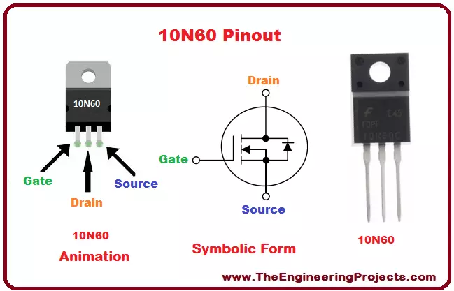
Hello everyone! I hope you all will be absolutely fine and having fun. Today, I am going to provide you a detailed discussion on
Introduction to 10N60. Before going into the details of this article you should also have a look at
Introduction to 4N60,
78M05,
2N3772,
2SC3320,
20N60. It is basically a high voltage Metal Oxide Semiconductor Field Effect Transistor (MOSFET). It is a power MOSFET and is able to control the certain level of the power. 10-N-60 is also a high current power MOSFET. This device has three terminals and is made up of silicon. It has around 10 ampere of current conduction capability i.e. this device is able to conduct 10A of current through it. 10-N-60 has a lot of amazing features.
It features include low on-state resistance, break down voltage up to 600 volts, fast switching speed, threshold up to 4 volts, avalanche energy fully specified, improved capability of dv/dt. It operates on 150 degree Celsius. Moreover, 10-N-60 has a wide range of application area including DC to DC converters, switched mode power supplies, Pulse Width Modulation (PWM) motor controllers, switched mode power supply, General Purpose (GP) switching appliances, bridge circuits and many more.
Introduction to 10N60
10N60 is basically a MOSFET having capability of bearing higher current and higher voltages. It is a power MOSFET i.e. it can control a power up to a specific level. It has three terminals named as gate, drain and source. It has several different features including fast switching speed, good dv/dt capability, low on state resistance, full avalanche energy specified. Its applications area include DC-DC converters, motor controllers, switched mode power supply, GP registers or appliances etc. 10-N-60 is shown in the figure given below.
1. 10N60 Pins
- It has three terminals having different individual task to perform.
- All of the three terminals are listed in the table given in the figure shown below.
2. 10N60 Pins Symbols
- In order to avoid the complexity, each terminal is assigned with an alphabetic character.
- The assigned alphabetic character assigned to each terminal are provided in the table shown in the figure given below.
3. 10N60 Symbolic Representation
- The symbolic representation of an electronic device provides us a symbol that can be used in theoretical portion.
- 10-N-60 symbolic representation is shown in the figure below.
4. 10N60 Pinout
- Pinout diagram of any electronic device helps to understand the pin configuration of that device.
- 10-N-60 pinout diagram is shown in the figure given below.
5. 10N60 Features
- The features are the parameters that can enhance the importance of any device in the market if they are unique.
- A device with more unique features will be more popular in the market.
- 10-N-60 features are provided in the table given in the figure shown below.
6. 10N60 Pins Applications
- It has a wide range of applications area.
- A few of its applications are listed in the table given in the figure shown below.
That is all from the tutorial
Introduction to 10N60. I have tried my level best to cover all the necessary and basic details regarding the basic use of 10-N-60 MOSFET. I hope you have enjoyed the tutorial and will appreciate my effort ;) If you found something missing or wrong in this article, please do let me know as soon as possible, so that the article can be updated correspondingly in order to avoid any type of future inconvenience. I will share further interesting and informative topics in my upcoming tutorials. So, till my next tutorial take care and bye bye :)
Introduction to 4N60
Hello everyone! I hope you will absolutely fine and having fun. Today, I am going to give you a detailed discussion on the topic
Introduction to 4N60. I have shared characteristics of the different IC's in my previous tutorials in
Introduction to 75N75,
SG3524,
2N3772,
L298,
L293D,
2SC3320 and
20N60. You must need to go through all these tutorials for the better understanding of today's article. 4N-60 is a high voltage Metal Oxide Semiconductor Field Effect Transistor (MOSFET). It is a three pin device including drain (
D), gate (
G) and source (
S).
4N60 is basically a power MOSFET and is able to handle the certain levels of power. It is specially designed to achieve the different characteristics e.g. high speed switching time, low charge on gate and low resistance for on state conditions. It also has highly rugged avalanche characteristics. 4N-60 has different amazing features e.g. capability of fast switching, avalanche energy specifications, higher ruggedness, improved capability for dv/dt. It has a wider range of real life applications including switching converters, switching regulators, relay drivers, solenoid, motor drivers and many more. The further detail about the basics usage of 4N-60 will be given later in this tutorial.
Introduction to 4N60
4N60 is basically a power MOSFET. It is a device having three pins named as gate, source and drain. It is designed to achieve high speed switching time characteristics and low charge on gate. It has different features including low on state resistance, highly avalanche energy specification, high ruggedness and many more. Its real life applications include motor drivers, solenoid, relay drivers, switching converters and a lot more. 4N-60 is shown in the figure given below.
1. 4N60 Pins
- This device has three (3) pins in total having different functions associated with each pin.
- All the three pins of 4N-60 are provided in the table given in the figure shown blow.
2. 4N60 Pins Symbols
- In order too avoid the complications, each pin is assigned with the first letter of its name.
- 4N-60 pin symbols are listed in the table given in the figure shown below.
3. 4N60 Symbolic Representation
- Symbolic representation is helpful to represent a particular device theoretically.
- 4N-60 symbolic representation is shown in the figure given below.
4. 4N60 Pinout
- Pinout diagram is helpful way to understand the pin configuration of any electronic device.
- I have also shared the pinout diagrams of different MOSFET's and IC's in Introduction to 50N06, IRFZ44N, C945, MC34063, NE555 and NE556, you must have a look at all these articles for the better understanding.
- 4N-60 pinout diagram is given in the figure shown below.
5. 4N60 Ratings
- Ratings show the power required to operate any electronic device.
- 4N-60 ratings are listed in the table given in the figure shown below.
6. 4N60 Features
- Features of a device play a vital role to make a device popular.
- 4N-60 common features are provided in the table given in the figure shown below.
7. 4N60 Applications
- It has a wider range of real life applications.
- Some of the most common applications are listed in the table shown in the figure given below.
That is all from the tutorial
Introduction to 4N60. I have tried my level best to provide all the necessary and basic information to use 4N60 for the first time. I hope you have enjoyed this tutorial and will appreciate my effort ;) If you have have any sort of problems regarding engineering issues, you can ask us in comments any without even feeling any kind of hesitation. Our team is 24/7 available for your support. I will share different interesting and informative topics in my upcoming tutorials. So, till my next article take care and bye bye :)
Introduction to 78M05
Hello everyone! I hope you will absolutely fine and having fun. Today, I am going to give you a detailed discussion on the topic
Introduction to 78M05. I have already shared information about different IC's e.g.
Introduction to UA741,
MMBD914,
LM224,
LM386 and
LM317. You must have a look at all these tutorials for the better understanding of this article. 78-M05 is basically a three (3) terminal. These terminals include input, output and the common terminal.
78-M05 is commonly available in TO-220 package having different fixed voltages at the output. Its construction process is based on planar epitaxial technology. These regulators are used for the employment of the process of internal limitation of the current. Safe area compensation as well as thermal shutdown are its more important features. 78-M05 is able provide up to 0.5A of current at the output, if the it is provided with the proper heat sinking. It is mostly known in the market on the basis of its fixed voltage regulation's applications. This shows that 78-M05 can be used with the external components in order to provide the adjustable voltage at the output. It has a lot of features. These features include thermal load internal protection, power molded packages, short circuit internal limitation of current, compatibility with Transistor Transistor Logic (TTL), Complementary Metal Oxide Semiconductor (CMOS) and different digital Integrated Circuits (IC's), complete protection for short circuiting, protection for thermal overload, Safe Operating Area (SOA) protection, outstanding ripples protection capability and many more. 78-M05 has a larger area for its real life applications including on card regulation, local regulation, it can be used with the external components to provide adjustable voltages at the output. The further detail about 78-M05 and its basic usage, will be provided later in this tutorial.
Introduction to 78M05
78M05 is a voltage regulator having three terminals. These terminal are input, common and the output terminal respectively. It is constructed using planar epitaxial manufacturing process. It is usually available in TO-220 packages. It has different unique features e.g. internal short circuit and thermal overload protection. It has a wide range of real life applications including local as well as on card regulation, current limitation and a lot more. Moreover, we can use it with different external components to achieve adjustable outputs. 78M-05 is given in the figure shown below.
1. 78M05 Pins
- It consists of three different terminals, having separate individual functions.
- All the terminals are provided in the table given in the figure shown below.
2. 78M05 Pins Description
- We must know about the function of each pin/terminal before using any device.
- The functions associated with each of the pin are listed in the table shown in the figure below.
3. 78M05 Circuit for Adjustable Output Voltage
- Adjustable output voltage circuit is shown in the figure given below.
4. 78M05 Pinout
- Before using a device, its pin configuration must be known.
- Pin configuration shows, where to supply power and from which pin we can get our desired output.
- Pinout diagram helps to understand the knowledge about pin configurations.
- I have also shared the pinout diagrams of LM339, LM393, BC547, IRF540, ULN2003 and LM117.
- 78-M05 pinout diagram is given in the figure shown below.
5. 78M05 Ratings
- Each device requires a certain level of power to be supplied.
- We must know about the level of power required to operate a particular device
- This power level can be estimated through the power ratings of that particular device.
- 78-M05 power ratings are provided in the table shown in the figure given below.
6. 78M05 Features
- A device can be made more popular just by making its features unique and vast. You should also read about BC557.
- 78-M05 common features are provided in the table given in the figure shown below.
7. 78M05 Applications
- The sale of a product in the market cam be related directly to its applications.
- More applications will automatically lead to the larger sale of a product.
- Applications associated with 78-M05 are listed in the table given in the figure shown below.
In the article
Introduction to 78M05, I have tried my level to provide all the necessary data about the voltage regulator 78-M05. Its pin configuration, features, pinout diagram, applications and many other parameters are provided in this tutorial. I hope you have enjoyed this article. If you have any problem, you can freely ask us in comments anytime. We are 24/7 available for your support. Our team will solve your issues to the best of their efforts. If you found something missing in this tutorial, please let us know. So, thaat it can be updated immediately to avoid any sort of future inconvenience.
Introduction to 2N3772
Hello friends! I hope you all will be absolutely fine and having fun. Today, I am going to give you an elaboration on
Introduction to 2N3772. I have already shared basic knowledge about different IC's and transistors in my previous tutorials e.g. Introduction to
IRF540,
BC547,
MMBD914,
LM339,
LM224 and
LM386. You must have alook at these tutorials before going into the details of this tutorials. It will be quite helpful in the better understanding of this article. 2N-3772 is basically a type of central semiconductor. It is basically a Negative Positive Negative (NPN) semiconductor. This semiconductor is designed by the process named as epitiaxial process. The main purpose behind its designing is to provide the high power based amplification process and fast switching applications.
The structure of 2N-3772 is mounted in JEDEC TO-3 metalic case. It is most suitable for inductive switching as well as linear amplifiers. 2N-3772 has a lot of amazing and unique features. These features include low saturation voltage for collector emitter junction. This voltage is around 4 volts. Capability of forward biased 2nd breakdown current is it another unique features among its competitors. 2N-3772 is also available in lead (Pb) free packages in the market these days. It has a wide range of applications in real life. Its most common real life applications include its use in linear amplifiers, fast switching devices, inductive switching, series pas regulators and many more that may be discussed later. This is the brief introduction to 2N3772. Thee further information about the basic use of 2N-3772 will be given later in this tutorial.
Introduction to 2N3772
2N3772 is an Negative Positive Negative (NPN) transistor. It belongs to the family of central semiconductors. It is enveloped in JEDEC TO-3 metalic structure. It is available at low cost while providing higher efficiency as compared to the other similar devices. It is easily available in the market and most of the time it is known on the basis of its applications. It has several different amazing features including low collector-emitter junction voltage, capable of forward biased current break-down. Its applications are include inductive switching, General Purpose (GP) linear amplifiers, series pas regulators and a lot more. "N-3772 is given in the figure shown below.
1. 2N3772 Pins
- Similar to the other transistor, it also has total three (3) pins.
- The names of all the pins are listed in the table given in the figure shown below.
2. 2N3772 Pin Symbols
- In order to avoid the complexity, each pin is simply assigned with the first letter of its name.
- The symbols assigned to each pin are provided in table given in the figure shown below.
3. 2N3772 Pin Symbolic Representation
- Symbolic representation of a device shows its symbol for theoretical use.
- 2N-3772 symbolic representation is shown in the figure below.
4. 2N3772 Pinout
- One must know about the pin configuration of any electronic device before using it.
- Pins configuration can be easily estimated via pinout diagram of an electronic device.
- I have also shared pinout diagram of different electronic devices in Introduction to L293D, L298, LM117, LM339, NE555, NE556, TL431 and TL072
- 2N-3772 pinout diagram is given in the figure shown below.
- From the above figure, you can see that I have provided the pins information as well as its real image for the better understanding.
5. 2N3772 Ratings
- Power requirements of each electronic device are very important parameters to operate them appropriately.
- If we don't know about the power requirements of a particular device, then providing slight higher voltage or current, it may be damaged immediately.
- Power requirements can be estimated from the power ratings of any device.
- Power ratings of 2N-3772 are listed in the table shown in the figure given below.
6. 2N3772 Electrical Characteristics
- It shows the electrical requirements of any electronic device.
- 2N-3772 electrical characteristics are listed in the table shown in the figure below.
7. 2N3772 Features
- Features belong to such parameters which are normally considered to be the most important key to success of any device while designing it.
- Unique features can make a device more popular.
- 2N-3772 common features are provided in the table shown in the figure given below.
8. 2N3772 Applications
- Applications are directly related to the popularity and sale of a product in the market.
- Larger the area of applications, higher will be chance of its sale.
- 2N-3772 application are listed in the table given in the figure shown below.
- Charging test time circuit for 2N-3772 is shown in the figure given below.
The tutorial
Introduction to 2N3772, has provided the platform consisting of all the necessary and important details about the basics of 2N3772, that one must know before its use. I hope you have enjoyed the tutorial. If there is something missing in this article, please do let me know. I will immediately update it correspondingly so that the future convenience can be avoided. If you have any sort of issue, you can ask us inn comments anytime you want to! Our team is 24/7 available to support you. We will try our level best to sort out your problems as soon as possible. I will share a lot of interesting as well as informative topics in my upcoming tutorials. So, till my next tutorial, take care and bye bye :)