Introduction to 74HC595

Hello everyone! I hope you will be absolutely fine and having fun. Today, I am going to explain all of you about
Introduction to 74HC595. It is basically a shift register. It has an ability to store and to shift the data of 8 bits. First of all the data is written on the register serially and then it goes to the storage register. All of the output lines are controlled by this register.
74HC595 register is a very high speed device based on Complementary Metal Oxide Semiconductor (CMOS). 8 bit data register receives the data from the input
DS. This data is then transferred from the input shift register to the output shift register. 74HC595 has a vey wide range of applications in daily life. It can be used as serial to parallel data converter, can receive and keeps the data for a long time etc. Moreover, It can be used in home appliances, for the industrial management, as computer peripheral. We will discuss further about this register later in this tutorial.
Introduction to 74HC595
74HC595 is a shift register having and eight bit storage register and an eight bit shift register. The data is written first and then stored into the device. It is high speed CMOS device. The data is usually entered in a serial format. Storage register is used to control the output lines of 74HC595. It has different real life applications e.g. in home appliances, computer peripherals, serial to parallel converter etc.
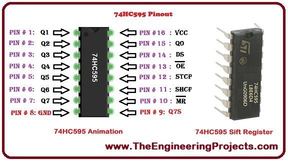
1. 74HC595 Pinout
- It has 16 pins in total out which eight are on left side and the remaining on the right side of the structure.
- The different function is associated with each of the pin.
- Some of the pins acts as an input to this device and receives data serially and transfer to the output pins to observe the received data.
- The pin diagram for 74HC595 is shown in the figure below:

- DS pin acts and receives the serial data.
- All of the lines with prefix Q acts as the output lines.
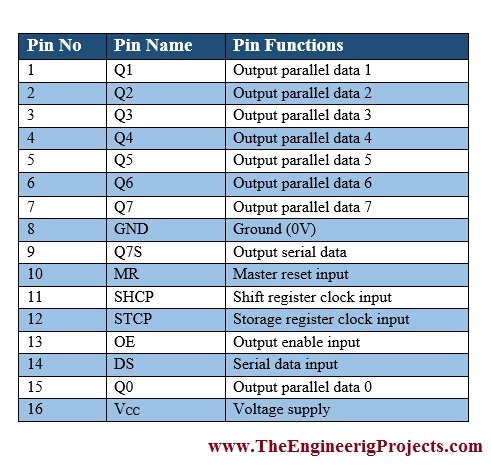
2. 74HC595 Pin Configuration
- In this section if the tutorial Introduction to 74HC595, I will tell you about the functions associated with each of the individual pin of 74HC595.
- All of the associated functions are describes in the table given below.

3. Functioning Diagarm
- The proper functional diagram of the shift register 74HC595 is shown in the figure below.
- From the above figure you can see that SHCP, master reset (MR) and the input DS are connected to 8 stage shift register.
- Pin number 12 i.e. STCP is connected to 8 bit storage register.
- The output enable (OE) is connected to 3 state outputs.
4. 74HC595 Functional Description
- In this section of the tutorial Introduction to 74HC595, I will tell you about the functions of each line of the 8 bit shift register 74HC595.
- Complete description of the functions of 74HC595 is given in the table shown below.
5. 74HC595 Timing Diagram
- The arrow in the upward direction shows the rising edge of the each wave either received or applied.
- The shape of the signals applied and received and their relation with each other is shown in the figure below.
5. 74HC595 Logic Diagram
- The logic diagram for 74HC595 8 bit shift register is shown in the figure below.
- You can see that there are 8 different stages from 0 to 7 and latches are there in the logic diagram of 74HC595.
- Output enable (OE) and master reset (MR) are connected to latches with an inverted sign usually known as bubble.
6. 74HC595 Current/Voltage Rating
- The current, power and voltage rating along with their values and system international units are shown in the table given below.
- The values of operating temperature and storage temperature are also shown in the figure below.
7. 74HC595 Proteus Simulation
- I have a Proteus simulation for continuous control of the different LED's using 74HC595.
- The screenshot of the simulation is shown in the figure below.
- The complete Arduino source code is shown below.
- You need to just upload .hex file of this code into the Arduino of Proteus and run the simulation.
int RCLK = 5;
int SER = 6;
int SRCLK = 7;

#define TotalIC 1
#define TotalICPins TotalIC * 8

boolean Data[TotalICPins];

void setup()
{
  pinMode(SER, OUTPUT);
  pinMode(RCLK, OUTPUT);
  pinMode(SRCLK, OUTPUT);

  ClearBuffer();
}


void loop()
{
   for(int i = TotalICPins - 1; i >=  0; i--)
   {
      Data[i] = HIGH;
      UpdateData();
      delay(300);
      ClearBuffer();
   }

   for(int i = 1;i < TotalICPins - 1;  i++)
   {
      Data[i] = HIGH;
      UpdateData();
      delay(300);
      ClearBuffer();
   }

}
- The running form of the above simulation is shown in the GIF below.
- You can download the complete simulation as well as the complete Arduino source code, here by clicking on the button below.
Proteus Simulation & Arduino Code
- Just download .rar file, extract it and enjoy the complete package having both Arduino source code as well as Proteus simulation.
So that is all from the tutorial
Introduction to 74HC595. I hope you really enjoyed this tutorial. If you face any sort of problem regarding any thing, you can ask me anytime in comments without even feeling any kind of hesitation. I will try my level to entertain you and to solve your issues in a better way, if possible. Our entire team is 24/7 here to entertain you and to solve your issues in a way or the other. I will explore different IC's in my later tutorials and will surely share all them with all of as you as well. So, till then, Take Care :)
Introduction to 2N3904
Hello everyone! I hope you will be absolutely fine and having fun. Today, I am going to give an
Introduction to 2N3904. It is basically an NPN transistor made up of silicon material. It acts as a general purpose amplifier and switch. You should also have a look at
Introduction to 2N2222, which is also an NPN transistor and considered as 2N3904 equivalent.
It is mostly used for lower power amplifiers and switching applications. Its major functional area is enclosed in TO-92 package. Its a silicon NPN general purpose bipolar junction (BJT) transistor designed for switching purpose as well as for an amplifier. Its can bear lower amount of current, lower power and medium voltage levels. It is most commonly used BJT due to its smaller size, wide availability and low cost. It is less sensitive to fluctuations in voltages and currents as compared to other BJT's.
| Where To Buy? |
|---|
| No. | Components | Distributor | Link To Buy |
| 1 | 2N3904 | Amazon | Buy Now |
Introduction to 2N3904
- 2N3904 is a silicon NPN Bipolar Junction Transistor (BJT), enclosed in TO-92 package and is normally used for switching & amplification purposes.
- 2N3904 Pinout consists of 3 Pins i.e. Base, Emitter & Collector.
- As it's an NPN transistor, so major charge carriers are electrons caryying negative charge.
- Small voltage at base(around 0.7V) changes its state from reverse to forward biased and starts conducting.
- It has a wide range of applications i.e. used in televisions, home appliances, medium-load switches, PWM applications etc.
Now let's have a look at 2n3904 Pinout:
2N3904 Pinout
- 2N3904 Pinout has three pins in total:
- Emitter denoted by E
- Base denoted by B.
- Collector denoted by C.
- 2N3904 Pin Diagram is shown in below figure:
- 2N3904 Pinouts alongwith their symbols are shown in the table given below.
Let's have a look at the Datasheet of 2N3904:
2N3904 Datasheet
- In order to get in-depth knowledge on any component, must read its datasheet. Here's the link to download 2n3904 Datasheet:
Introduction to 2N3904
Let's have a look at the equivalents of 2N3904 NPN Transistor:
2N3904 Equivalent
Although common transistors such as 2N3904 are easily available in local/online electronics stores, but its wise to know the alternatives. So, 2N3904 equivalents are as follows:
- BC636
- 2N3055
- 2N2222
- BC549
- BC639
- 2SC5200
- 2N2369
- 2N3906
Now let's have a look at poewr ratings of 2N3904:
2N3904 Ratings
- Transistors are available in different ranges of power ratings and their selection depends on circuit's requirements.
- So, a circuit designer's task is to select an optimized transistor for its circuit, which should fullfill all its power equirements & must be cost efficient.
- If current/voltage passing through a transistor exceeds its ratings, the transistor may burnt out.
- Below table shows 2N3904 Ratings:
| 2N3904 Ratings |
| No. |
Parameter Name |
Parameter Value |
| 1 |
C-E Voltage (VCEO) |
40V (DC) |
| 2 |
C-B Voltage (VCBO) |
60V (DC) |
| 3 |
E-B Voltage (VEBO) |
6V (DC) |
| 4 |
Collector Current (IC) |
200mA |
Now, let's have a look at few applications of 2N3904:
2N3904 Applications
2N3904 is one of the most commonly used NPN transistor because of its low-cost, high-speed and small-size. Few of 2N3904 applications are as follows:
- It's normally used as a simple switch to control heavy loads, because of its low saturation voltage and high gain.
- It's used in home appliances i.e. TV, LCDs, stereo systems etc.
- It's also used in fast switching applications i.e. pulse width modulation(pwm), because of its fast switching speed.
- 2N3904 is also in signal amplification projects(i.e. sound amplifiers) as it has high current gain & thus can be used as an amplifier.
2N3904 Transistor as a switch
- In normal state, 2N3904 acts as reverse biased and there's no conduction between Collector & Emitter.
- When small voltage applies at its Base Terminal(normally 5V), 2N3904 converts its state from reverse to forward biased and conventional current starts flowing from Collector to Emitter.
Now, let's design a simulation to practically understand, how 2N3904 transistor acts as a switch?
2N3904 Proteus Simulation
- Let's first control a simple LED on/off state using 2N3904 NPN transistor
- As shown in below figure, power is supplied at Collector and LED is connected at the Emitter with resistor(to limit current) & grounded from the other end.
- As there's no voltage applied at Base Terminal, so 2N3904 is reverse biased and thus LED is OFF.
- Now when we have applied 5V at Base Terminal(using LogicState in Proteus), 2N3904 gets forward biased and now LED is ON, as shown in below figure:
- So, that's how we can use 2N3904 transistor as a switch.
In above simulation, we have controlled a simple LED and have used a manual switch. Now, I am going to control a DC motor with Arduino.
2N3904 Arduino Interfacing in Proteus
- I have made another simulation in Proteus ISIS for DC motor control using 2N3904.
- The screenshot of the simulation is shown in the figure below.
- The complete Arduino source code of the above simulation is given below.
- You have to get the hex file in Arduino to observe the results properly.
int MotorInput = 2;
int MotorOutput = 7;

void setup()
{
    pinMode(MotorInput, INPUT_PULLUP);
    pinMode(MotorOutput , OUTPUT);
}

void loop()
{
    if(digitalRead(MotorInput) == HIGH)
    {
      digitalWrite(MotorOutput, HIGH);
    }
    if(digitalRead(MotorInput) == LOW)
    {
      digitalWrite(MotorOutput, LOW);
    }

}
- The running form of the above simulation is shown in the below figure:
- From the above figure you can see that after uploading .hex file and running the simulation you need to change the level of logic state from 0 to 1, and the motor will start to rotate.
- You can download the complete Proteus ISIS simulation as well as complete Arduino source code, here by clicking on the button below.
- Just download .rar file, extract it and enjoy the complete package.
Introduction to 2N3904
- You should watch this below video to understand how to run this Proteus Simulation:
So that is all from the tutorial
Introduction to 2N3904. I hope you really enjoyed this tutorial. If you face any sort of problem regarding any thing, you can ask me anytime in comments without even feeling any kind of hesitation. I will try my level to entertain you and to solve your issues in a better way, if possible. Our entire team is 24/7 here to entertain you and to solve your issues in a way or the other. I will explore different IC's in my later tutorials and will surely share all them with all of as you as well. So, till then, Take Care :)
Introduction to 1N4148
Hello everyone! I hope you will be absolutely fine and having fun. Today, I am going to give an
Introduction to 1N4148. It is basically a diode used for fast switching purposes. Switching diodes are usually single P-N diodes and their functionality is similar to that of normal switch.
Below a specific voltage, switching diodes i.e. 1N4148 has high resistance. Whereas as above that specific voltage they show a low resistance. It is a most commonly used diode due to its smaller size, easy availability and low cost. Good switching diode can be chosen by its maximum reverse recovery time and its power dissipation ranging from 80mW to 1kW. Switching diodes such as 1N4148,
1N4007 etc. have very wide range of applications specially in
Embedded Systems for switching purposes. It is mostly used in switches having extremely fast operation. It can be used for high speed rectification, general purpose switching and fast switching are also included in its applications, protection of telecommunication industries and homes etc.
Introduction to 1N4148
1N4148 is a standard diode made up of silicon and is used for extremely fast switching operations. It has two modes of operation named as:
- Forward Biased
- Reverse Baised
In Forward Biased operational mode, it allows the current to pass though it and it acts as a closed switch, while in Reverse Biased operational mode it acts as an open switch and doesn't allow the current to pass through it. I have explained it in below figure:
I have designed the above simulation in
Proteus and you can see in the above image.
- In forward biased state, diode IN4148 is acting as a closed switch and allowing the current to pass through it, that's why our LED is ON.
- In Reversed Biased state, diode IN4148 is acting as an open switch and there's no current flowing through it, that's why our LED is OFF.
- In the below figure, I have shown the equivalent circuit of both of these diode states:
1. 1N4148 Mechanical Design Parameters
- The different parameters for mechanical design of this diode are shown in the table given below.
- These are few of the parameters for mechanical designing of the zener diode 1N4148.
- Some of the other mechanical parameters are also shown in the table given below.
- The parameters given in the table above can be verified from the figure shown below,
- From the figure shown above, we can see that the diode has four major sides which are A, B, C and D respectively.
- Each of the side has its own different dimension as given in the table shown above.
- So, that was the brief discussion about the mechanical design parameters for this diode.
2. 1N4148 Pinout
- 1N4148 has only a single input terminal and a single output terminal.
- Input terminal is known as anode and output terminal is known as cathode.
- Anode is indicated by the positive (?ve) charge whereas the cathode is indicated by negative (?ve) charge.
- Pins and their charges are shown in the table given below.
3. 1N4148 Pins Diagram
- Pins diagram for this diode is shown in the figure below,
- This is the properly labeled diagram of 1N4148 showing anode on one side as A and cathode on the other side as B.
4. 1N4148 Power Ratings
- The current, voltage and power rating for the diode 1N4148 are provided in the table shown below.
- The table above displays the ratings of the particular diode along with their symbols and values.
5. 1N4148 Applications
The switching diode i.e. 1N4148 has a wide range of applications, a few pf which are given below:
- Extremely fat switching purposes.
- High speed rectification.
- General purpose switching.
- Protection circuits in telecommunication industries, offices, homes etc.
- These were few of the applications associated with this switching diode.
So that is all from the tutorial
Introduction to 1N4148. I hope you really enjoyed this tutorial. If you face any sort of problem regarding any thing, you can ask me anytime in comments without even feeling any kind of hesitation. I will try my level to entertain you and to solve your issues in a better way, if possible. Our entire team is 24/7 here to entertain you and to solve your issues in a way or the other. I will explore different IC's in my later tutorials and will surely share all them with all of as you as well. So, till then, Take Care :)
