Hello Friends! Hope you’re well today. I welcome you on board. In this post today, I’ll walk you through the Introduction to 2SC1061.2sc1601 is an NPN bipolar junction transistor used for switching and amplification purposes. During the amplification process, the small input current across one pair of terminals is used to generate a large output current across other pairs of terminals.
2sc1601 is known as a semiconductor device made of silicon material. This is a bipolar junction transistor where two charge carriers (electrons and holes) play an important role in the conductivity inside the transistor. As this is an NPN transistor so here major charge carriers are electrons while holes are the minority carriers.
I suggest you buckle up as I’ll detail the complete Introduction to 2SC1 ...
Hello! I welcome you to the board. We'll talk about the Solar Panels and their wattage to choose the solar panel according to the need of the time. The performance and efficiency of a home power plant directly depend on the correct choice of solar panel characteristics. Innovative technology has made it possible to create a record 400-watt solar panel, which is currently the most efficient and economical. To determine the number and capacity of solar panels, it is necessary to accurately calculate the total energy consumption and choose the right type of panel.
Choose the Type
To determine the number and capacity of solar panels, it is necessary to accurately calculate the total energy consumption and choose the right type of panel. There are 2 ...
Hello Reader! Welcome to The Engineering Projects. At the present time, we'll discuss the client invoice and the tips and tricks to manage your client invoice service. We all know Payment matters are always a bit of an issue when it comes to closing a deal. One way or another, we all work to get a further reward and mostly it is about money. Usually, the system of client invoices is pretty much tuned.However, a certain need for better optimization from time to time pops its head up. To avoid extra stress, you might want to look through the information below and get some inspiration on how to improve your invoice arrangements. You should also visit Zintego to find free Invoice templates.
Comprehend the importance of an invoice
Invoices are meant ...
Hello friends, I hope you all are doing great. In today's tutorial, I am going to share Top 5 Reasons a Survivalist Should Be an Amateur Radio Operator. With 2021 setting in, are you well prepared to survive if the world goes down? We live in uncertain times, and the pandemic has taught us that what we plan today might not be applicable tomorrow. Simply put, like survivalists, we should be mentally and physically tough and all geared-up for emergencies, disruptions, and the breakdown of society. If you are currently living the survival mode, also known as the prepper lifestyle, you are heavily self-reliant. We expect you to have your backpack ready with all the right emergency tools and gadgets, such as a survival knife and a ham radio set. Read ...
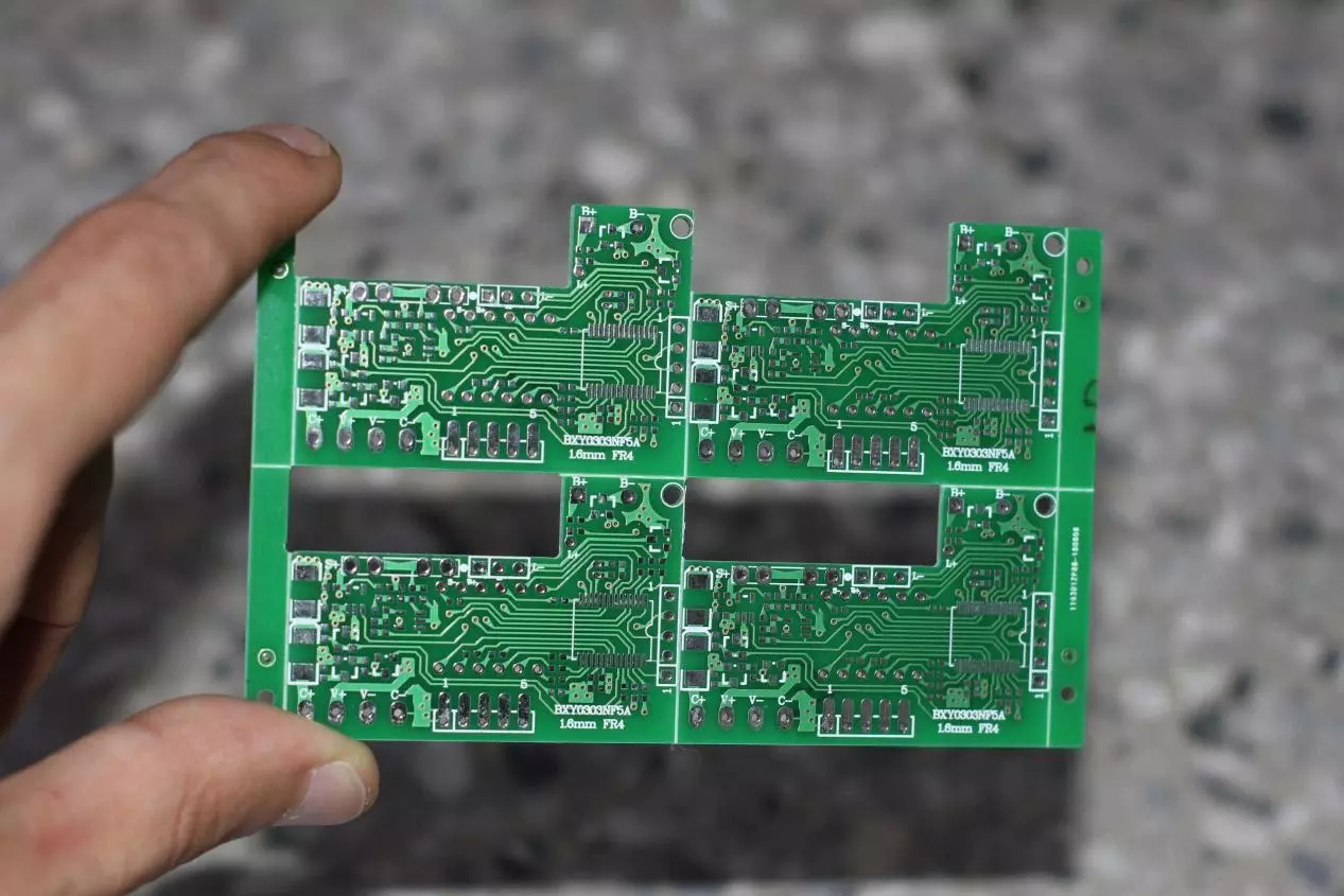
Hello Professional! Welcome to The Engineering Projects. We hope you are having a productive day. Today we'll talk about the building process of Printed Circuit Board with great efficiency and creativity.
It's hard-won to run an industrial company. What’s the reason? One is the bosses who have earned money quickly expand their business footprint not only focus on PCB, not delve into how to provide higher-quality PCB and more extreme customer service; also many bosses think more about engaging in financing and listing. How about JLCPCB?Yes, JLCPCB has planted into the PCB with all its heart, just keeping one aim: build the PCB best.
JLCPCB was founded in 2006, used to be the leading PCB company, now it is PCB industry big brother, who is highly appreciated and trusted by hardware fiel ...
Hello Guys! Hope you’re well today. I welcome you on board. In this post today I’ll describe the Introduction to IRF3710.The IRF3710 is an N-channel MOSFET made up using advanced process technology. It is mainly used for fast switching purposes and comes with extremely low on-resistance. It is a fully avalanche-rated device with a gate-source voltage of around 20V.
I suggest you read this entire post till the end as I’ll detail the complete Introduction to IRF3710 covering datasheet, pinout, features, and applications.
Let’s jump right in.
Introduction to IRF3710
The IRF3710 is an N-channel MOSFET mainly employed for fast-switching purposes.
It is manufactured using advanced process technology and comes with very low on-resistance.
This device is composed of three termina ...
Hey Readers! I welcome you on the board. I hope you are doing Great. are you establishing a new office? or you want creative ideas about your Office? or you just want to get the concepts about the Modern office requirement? then I can help you.
Office designs continue to change with modern trends, and there are many aspects of office design that can even have an impact on the productivity of the people who work there.
It is more important than ever that the office environment is a welcoming one to ensure that every staff member will be able to give their best in terms of collaboration and work, and there are a number of things that every modern office needs - everything from spatial design to using LED strip lights.
A varied and comfortable wor ...
Hey Pals! We hope you are doing Great. Today, we are going to design another application of DLD Logical Gates i.e. Half Subtractor. In our previous lectures, we covered Adders in detail, where we studied both Half Adders & Full Adders. Now its time to discuss its reciprocal i.e. Subtractors.
In this session, we'll seek the answers to the following topics:
What is Half Subtractor?
Working Principle of Half Subtractor.
Truth-table of Half Subtractor.
Simulation of Half Subtractor in Proteus using three Logic Gates.
Designing of Half Subtractor with NOR gate.
So, let's get started:
What is Subtractor?The functionality of Subtractors is exactly the opposite of Adders(we discussed in previous lectures) and defined as:A Subtractor is a simple DLD Electronic circuit, d ...
Hello Learners! We welcome you on the Board. We hope you are doing Great. Today we'll talk about the Tips that will be useful and functional Tips that will work best for you if you are thinking to shift in the new build.
If statistics are to be believed, the UK is something of a new-build heaven. Every year an estimated 247,000 more houses are built than demolished. On the face of things, new-build properties seem the dream. Remember the days of worrying about a lack of damp-proof course in older properties. Or, what about that chimney stack that can't be moved, but acts as a total eyesore in your front room.
While more traditional problems might have been erased, new ones have come in their place. Today's guide is all about showcasing how you ca ...
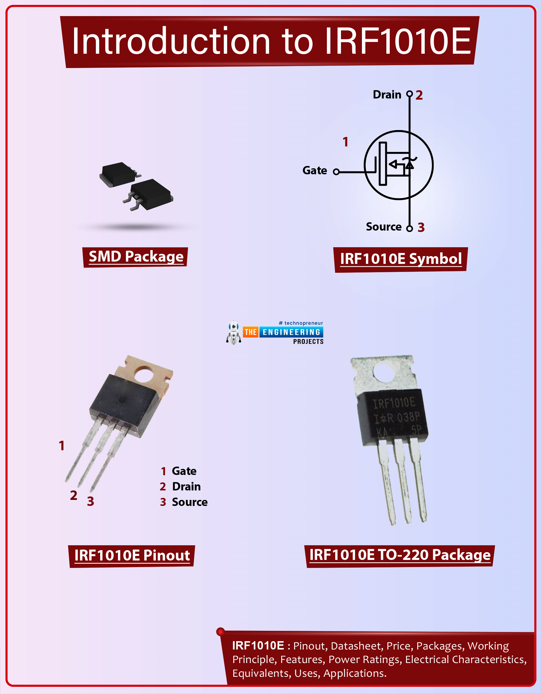
Hi Guys! I welcome you on board. Happy to see you around. In this post today, I’ll walk you through the Introduction to IRF1010E.The IRF1010E is an N-channel power MOSFET that comes with low turn-on resistance and is mainly used in fast-switching applications. The maximum power dissipation of this device is 170W and the pulsed drain current is quite high i.e. 330A.
I suggest you buckle up as I’ll detail the complete Introduction to IRF1010E covering datasheet, pinout, features, and applications.
Let’s get started.
Introduction to IRF1010E
The IRF1010E is an N-channel power MOSFET mainly employed for fast-switching applications.
This chip is a three-terminal device with terminals drain, source, and gate. It is a voltage-controlled device as opposed to a bipolar junction trans ...