LendInvest makes property finance simpler. Bridging loans, development finance, and buy-to-let mortgages for intermediaries, landlords, and developers made it easier. LendInvest provides loans that you can trust. They provide fast and flexible funding to help the property professionals create housing that is funded by an international capital base. LendInvest’s international capital base of £2 billion supports projects of wide variety and they are backed by some of the world’s largest financial institutions and the most successful individuals. Some institutions include HSBC, J.P. Morgan, Citi, and NAB. Be updated in banking news to learn more.
How do they simplify property finance? They use technology-enabled lending and they are relationship focu ...
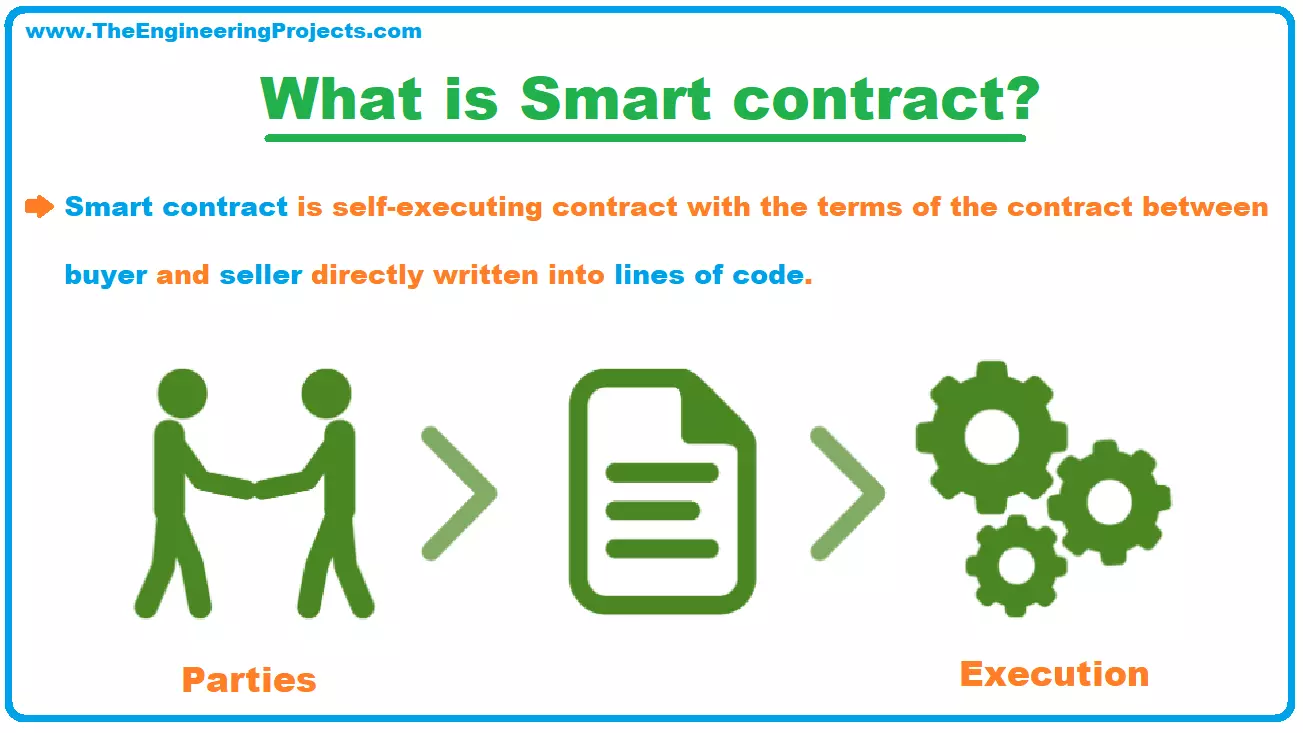
Hello friends, Hope you are doing fine and having a good time in your life. The topic that I am going to discuss today is a very interesting and important one in the context of blockchain. I will discuss smart contracts in this article and I am sure you will learn the concept by the end of this tutorial. I have mentioned smart contracts in my previous articles and defined them before.
Before discussing smart contracts, let’s first revise what a contract is, and then we will talk about smart contracts.
Contract
When two persons or two parties want to carry out a deal or a transaction such as buying property, they need some proof for future reference.
So, a contract between two or more individuals is a legal document that serves as proof for t ...
Hello friends, hope you are doing fine and enjoying your life. In today’s article, I am going to discuss decentralized applications that are abbreviated as dApps. With the invention of blockchain technology and afterward Ethereum, the idea of decentralized applications has gained a lot of attention. So let’s get into the details and learn what a dApp is.
Decentralized Applications (dApps)
An application built on a decentralized platform such as Ethereum is called a Decentralized Application(dApp).
A dApp generally consists of a backend and a frontend.
The backend of a dApp is a smart contract mostly written in solidity language.
The front end of a decentralized application is the user in ...
Hello friends, hope you are doing good and enjoying your life. Today, I am going to introduce you to the Ethereum wallets. I have given you an introduction to blockchain, its characteristics, and an introduction to accounts in my previous tutorials, so let’s get started with today’s tutorial on Ethereum wallets.
What is Ethereum Wallet???
In this section, I will introduce you to the Ethereum wallet and then we will move into its further details.
A blockchain wallet is just like a real-life wallet but in software form. It is the digital form of a wallet.
A wallet is application software that acts as a user interface to the Ethereum network.
The wallet is a system to manage and store the keys.
This digital wallet allows transferring crypto ...
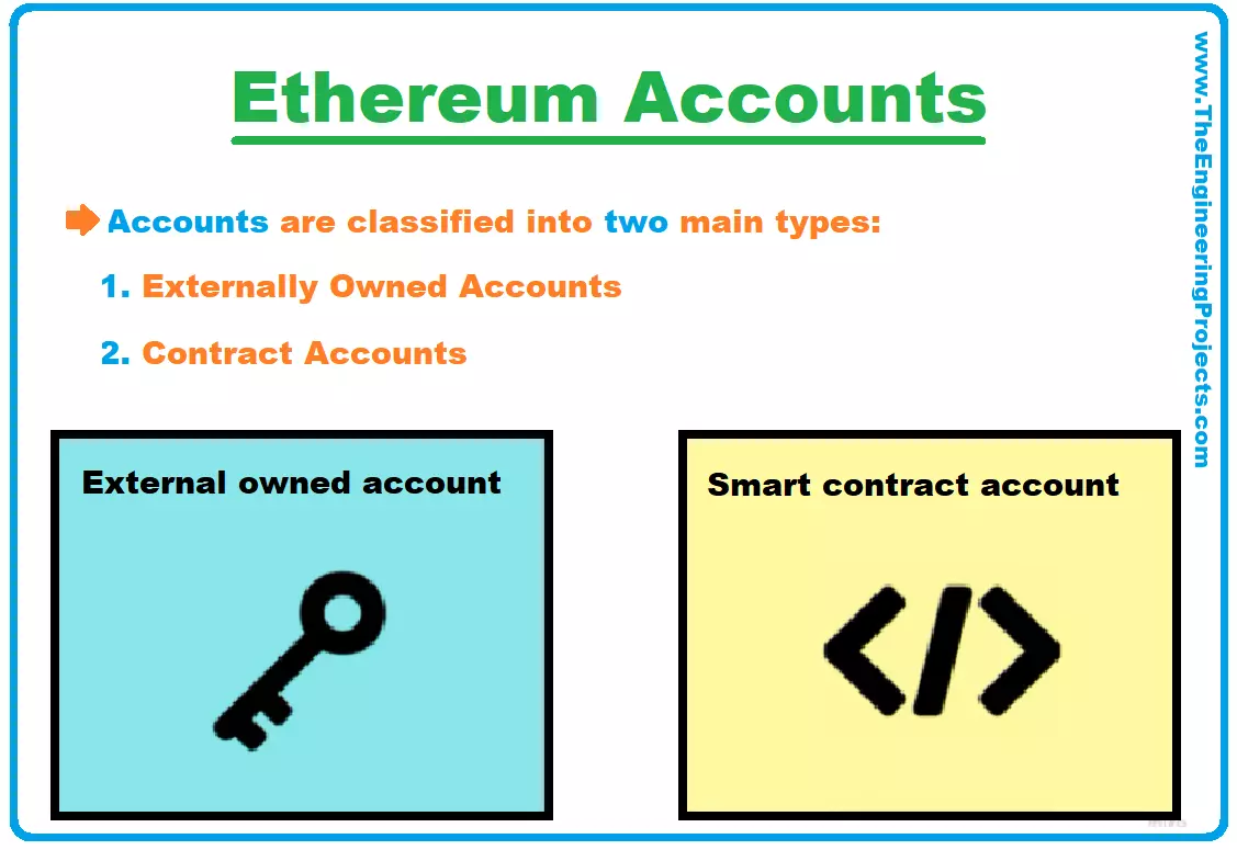
Hello friends, hope you are doing good and enjoying your life. Today, I am going to introduce you to Ethereum accounts. I have given you an introduction to blockchain in my previous tutorials, so let’s get started on the essentials of this technology. I am going to start with accounts.
Ethereum Accounts
An account is an important component of the Ethereum system.
It is the main building block and has a balance in ether (ETH) (Ethereum currency).
An account is capable of sending transactions on the Ethereum network.
The interactions between different accounts create transactions that are stored in the distributed database.
Each transaction involves the sender account, receiver account and contract account.
An account can be controlled b ...
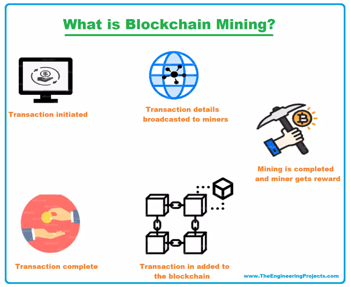
Hello Friends, Hope you are doing fine and having fun in your lives. In my previous tutorials on blockchain and Ethereum, I have talked about mining a few times. So, in today’s article, I am going to discuss the concept of mining with you. This is an important part of learning the working of blockchain to see how the decentralization of blockchain happens. Let’s start today’s article by defining mining.
Blockchain Mining
As blockchain is a peer-to-peer network. Mining is also a peer-to-peer process.
Blockchain (or Ethereum) mining is used to verify transactions on the network.
In this process, miners (the person or node who performs mining) add transaction records to the decentralized distributed ...
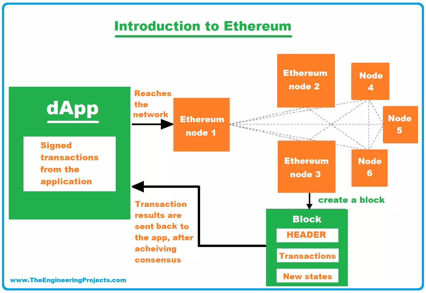
Hello friends, Hope you are doing good. In my last tutorial, I gave you an introduction to blockchain technology and this article is the second one of this series. Today I am going to talk about Ethereum. In simple words, Ethereum is an open-source platform of blockchain technology. But unlike the bitcoin blockchain, it offers more functionality. The blockchain in bitcoin tracks bitcoins only. It tracks the ownership and transfer of bitcoins. While Ethereum is not only a payment network for cryptocurrency but also termed as the world computer due to its wide functionality. First, let’s go through the key introductory points of Ethereum, and then we will dive into the details:
What is Ethereum Blockchain?
Ethereum blockchain is an open-source g ...
Hi friends, hope you are doing well. I have given you an introduction to Blockchain Technology and ethereum in my previous tutorials. In today’s article, I am going to talk about the characteristics of blockchain. There are several key characteristics of blockchain technology that make it different and usable from other technologies.
The architecture of blockchain is so unique that it inherently provides a lot of features to this technology. These features have benefits for several areas and sectors so let’s discuss these characteristic features.
Characteristics of Blockchain
We have already discussed the components of Blockchain in our previous tutorial Introduction to BlockChain Technology. Now, let's understand the characteristics of Blockchain ...
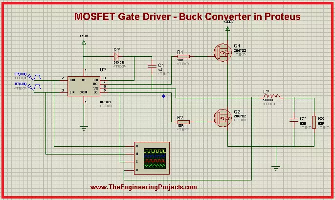
Hey Geeks! Welcome to The Engineering Projects. We hope you are doing great. MOSFET is a predominant component widely used in electronics due to its performance. We are working on the Projects of MOSFET and today's experiment is really interesting. We are working on the MOSFET Gate Driver and we will work on the following concepts:
Introduction to MOSFET Gate Driver.
Circuit of MOSFET Gate Driver.
Working of MOSFET Gate Driver.
Simulation of MOSFET Gate Driver in Proteus.
Applications of MOSFET Gate Driver.
You will find important information about the topic in DID YOU KNOW sections.
Introduction to MOSFET Gate Driver
We all know MOSFET is a type of transistor and is used in a wide range of circuits. It has many interesting features and ...
Hello friends, Hope you are doing good. Today I am going to talk about the technology that is most hyped right now and is said to bring revolution to the internet. Yes, I am talking about Blockchain technology and I am going to start explaining it from the very basics. Let’s start with a little history here without getting into too many details of it.
The concept of blockchain was introduced to the world by Satoshi Nakamoto although this concept was first described in 1991. The technology was introduced via bitcoin which is a cryptocurrency invented in 2008. You must have heard about this cryptocurrency already. Now I am going to move towards the introduction of blockchain in the next section.
What is Blockchain Technology?
Blockchain is a dis ...