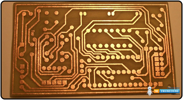
Hello everyone, I hope you all are doing well. In today’s tutorial, we are going to discuss the PCB Etching process, a fundamental step in PCB manufacturing. The PCB Etching process is used to remove the unwanted copper from the PCB surface to reveal the desired circuit pattern.
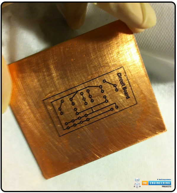
As we know, a PCB board has a complete copper layer in its raw form. We design our circuit in the software(i.e. Eagle, Altium, Proteus etc.) and place the pattern on the PCB board. This circuit pattern is normally protected by the tin plating, as shown in the below figure:
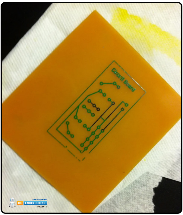
Now, there’s a need to remove the extra/unwanted copper layer from the PCB board and this process is called the PCB Etching Process. PCB Etching is carried out in various ways and the most commonly used is the Chemical Etching Process, where a chemical named Ferric Chloride is used to remove the copper. A completely Etched PCB is shown in the below figure:
Finally, we can remove the tin layer, polish the leftover copper layer (of our circuit), drill the holes and our PCB is ready for component placing & soldering.
Where to Order High-Quality Etching for PCBs
PCBway is the leading PCB manufacturing platform that offers all PCB services, from fabrication to assembly, in mass production with instant quotes. We ensure a smooth order process and one-on-one assistance for all your PCB manufacturing services, with the best value in direct pricing. We use modern technology and processes for PCB etching; therefore, we provide a wide range of etching techniques, including laser etching, chemical etching, and much more, to ensure the exact product you are searching for.
At PCBway Fabrication House, they provide real-time fabrication tracking for your orders so you can get the most satisfying and quick ordering process. Our professional workers know etching is a crucial step in PCB fabrication, and with the modernization of PCBs, they are becoming compact and complex, so etching provides accuracy and precision in the circuit design. Therefore, they follow the best practices and always get positive feedback for the services. For more information, follow the website’s link, and here is the main page:
The safe payment method and worldwide delivery are our prestige to satisfy the customers and work on bulk orders with the buyer’s protection. We deal with every type of PCB and provide multiple packages to grab the attention of every type of buyer.
In this article, I am going to discuss the introduction, types, workings, and other basic information that you must know before you get started with the etching process.
Introduction to the PCB Etching Process
PCB etching is a highly intricate process in PCB fabrication that involves the removal of unwanted material from the PCB surface. It is the controlled dissolution or erosion of unwanted copper where the specific PCB areas of the copper layer are removed to get the required pattern. It is also termed PCB printing, where circuit patterns are designed on the surface for the electric components.
Before starting the PCB etching, there is a need to create the layout of the desired design for the board. Great care is required to create the exact design and layout, and then, it is transferred onto the PCB through a process known as photolithography. During this step, the PCB is coated with light-sensitive materials, and the pattern is then transferred to the board using light. As a result, the blueprint of the design is ready to be etched with sharp results.

PCB etching is part of the manufacturing stage of PCBs, and it takes place just before the electronic components are mounted on them. This crucial part forms the pathways necessary for PCB operations by defining the electronic connections. It is considered the last stage of PCB fabrication, and then the board is moved towards the assembly stage.
PCB Etching Processes
As discussed before, etching is the fundamental part of PCB manufacturing. For that reason, various etching techniques are employed for the specific type and material of the board. Understanding each of them ensures the manufacturer gets the required output and sharp design. Etching is broadly characterized into two major classes:
Wet etching
Dry etching
Let’s discover both these classes and the methods related to them.
Wet Etching
The wet etching removes the undesired material from the PCB through chemical reactions. The next section will elaborate on its workings:
Wet Etching Working on PCB
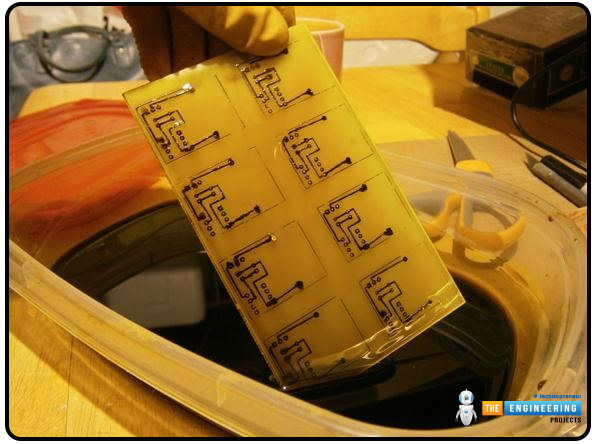
An etchant is a chemical substance that is used in the wet etching process to react with and dissolve the excessive material on the masked PCB. It is usually in liquid form; therefore, this type of etching is known as wet etching. Mainly, the etchants used in this method are acids, bases, or other solvents, and the selection of the right etchant depends on the type of PCB, masking, and some other important parameters. The following steps are required in wet etching:
Surface Preparation in Wet Etching
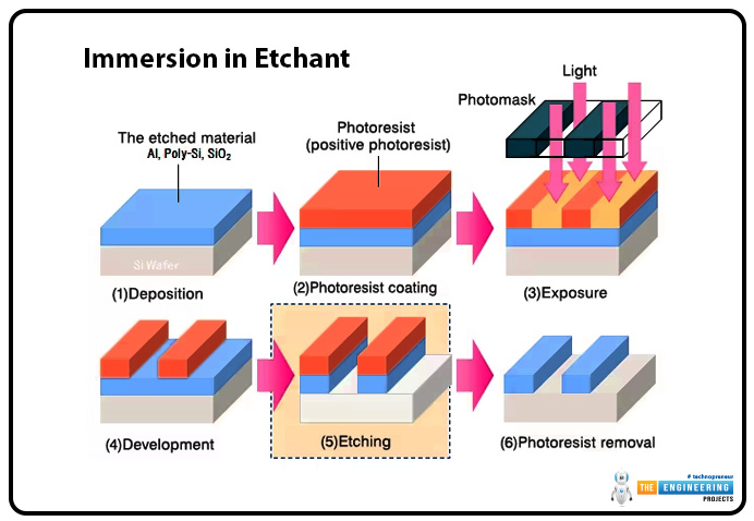
The patterns we see on the PCB are formed by a layer of metal or oxide on the surface. At the start, a plain layer of this material is coated on the PCB along with the photoresists (coating layer) through photolithography. As a result, only the dischargeable areas of metal or oxide are exposed for the etching.
Immersion in Etchant
Now, when the board is ready for the dissolving process, it is immersed in the etchant bath, where the exposed material undergoes the reaction process. Usually, the metal layer made of copper and ferric chloride is the etchant. This is a relatively time-consuming process, and the total time depends on the type of etchant used in this step. As a result, the underlying layer starts showing. At this point, it is important to take the board out of the etchant solution bath.
Rinsing and Cleaning in Wet Etching
After removing the substrate from the etchant solution, the board is thoroughly washed with water or other neutralizing agent to stop the chemical reaction.
Photoresist Removal in Wet Etching
This is the final step in this process, in which the photoresist layer is stripped away from the board and the user sees the desired pattern on the board.
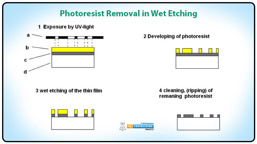
Wet etching is a simple and effective method to get a precise design, but it requires a lot of care to avoid over-etching or underlying layer damage. Generally, the wet etching is isotropic, which means it etches in all directions. It requires a less complicated method and does not have strong ions; therefore, it has a low risk of board damage.
Types of Wet Etching Processes
The following are the most common wet etching types:
Alkaline Etching on the PCB
The alkaline etching, or alkaline permanganate etching, utilizes an alkaline solution, usually NaOH (sodium hydroxide) and potassium permanganate (KMnO4). The solution dissolves the copper from the PCB, and this process is known for providing uniform etching at a high etching rate.
Usually, the manufacturers select this etching type in high-pressure and conveyorized chambers to improve efficiency and reaction rate. It is a good option for etching PCBs with an uncomplicated etching design and larger surface areas. Exposing the PCB to the refreshed etch spray within the chamber helps the manufacturer achieve less toxicity than with many other etching processes.
Acidic Etching in PCB
Acidic etching on PCB involves etching away unwanted copper from the surface through the chemical reaction of the acidic solution. The acidic solution can be applied to the PCB through different means, such as dipping it in the bath, spraying the solution on the board, or brushing it on the surface.
Once the acidic solution dissolves all the discardable copper layer areas, it is then washed and dried completely to stop the chemical reaction. Generally, the acidic method is considered best for the inner layer as it helps minimize the lateral erosion of the etched material of the masked metal layer. The chemical reaction is more controlled in this type; therefore, it provides an intricate and refined circuitry design. Manufacturers consider this method for smaller designs and dense boards because it provides a fine line width.
Dry Etching in PCB
Dry etching is a technique in PCB that involves the removal of unwanted metal coating areas through reactive gases or plasma instead of liquid chemical reactions. It is a highly precise method to create sharp patterns and fine features on PCB. The most common methods of dry etching are described next:
Plasma Etching on the PCB
Plasma etching has been used for PCBs since the 1960s but was not a prominent technique until the 1970s. This method was considered useful for reducing liquid waste disposal and getting sharper results as compared to wet etching. Another prominent benefit of using plasma etching is that it uses excitation and dissociation techniques to remove a particular part without causing damage to PCB surfaces. As a result, it is considered a good option for sensitive and delicate PCBs.
The method involves the use of a plasma system, also known as the plasma chamber. A high voltage is applied to the reactive gases such as oxygen (O2), chlorine (Cl2), argon, fluorine, etc., which break down the molecules into the constituent gas atoms. For this, the plasma system has a radio frequency source that produces electromagnetic waves. Some of these atoms are ionized (acquire charge) and then react with the exposed metal layer. As a result, the discardable copper molecules are broken down and removed. Mostly, the frequency range is 13.56 Mhz, 40 Khz, 80 Khz, 100 Khz, and 2.45 GHz.
The process does not involve any chemicals and is a dry, clean, and effective method for etching. The positive points of this method are that it is a clean, controlled, and precise method for etching that can be applied on small scales. Unlike some other techniques, there is no risk of vias contamination or solvent absorption. Moreover, it works better on high-density printed circuit boards, often utilized for fine-line circuitry. On the contrary, it is an incredibly costly technique and is not profitable until the etching is done in large quantities regularly. The chamber system requires maintenance and expertise.
Laser Etching on the PCB
Laser etching is also termed laser ablation or laser direct imaging (LDI) and was used at the start of 1987. It is the process in which a high-power laser beam is incident to the PCB surface to remove the unwanted copper layer and get pinpoint accuracy. It is a computer-controlled method, and the excessive copper is either evaporated entirely or flaked off.
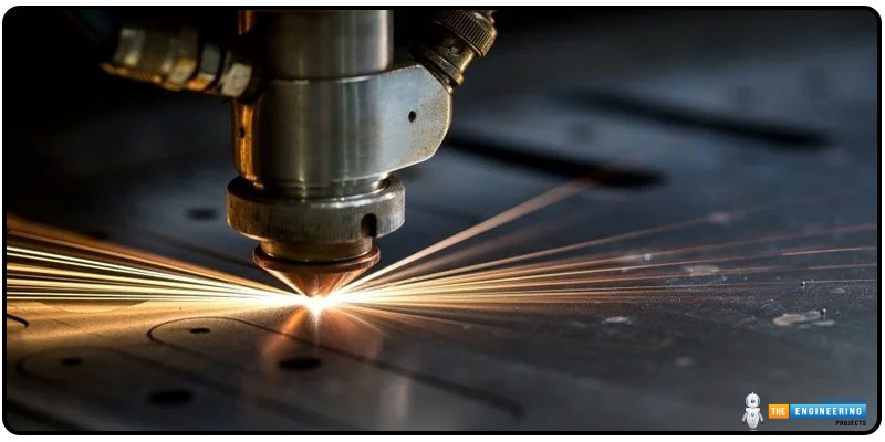
On a larger scale, laser etching has the following sub-types:
Fiber Laser
Ultra Violet Laser
CO2 Laser
Ventilation, eye protection, protective clothes, laser beam reflection maintenance, and limited direction viewing are some of the fundamental precautions required to apply this method. A benefit to using this method is that the number of steps in the whole process is very minimal if all the precautions and machinery are ready to use. No ink, acid, toxic material, or wet chemical is required for this process.
The disadvantage is, that etching the large board is challenging. Moreover, it requires a lot of investment at the start to get the equipment and system ready. The operational cost is also high in this process.
Comparing Wet Etching and Dry Etching
The following table shows the difference between wet and dry etching for the printed circuit board:
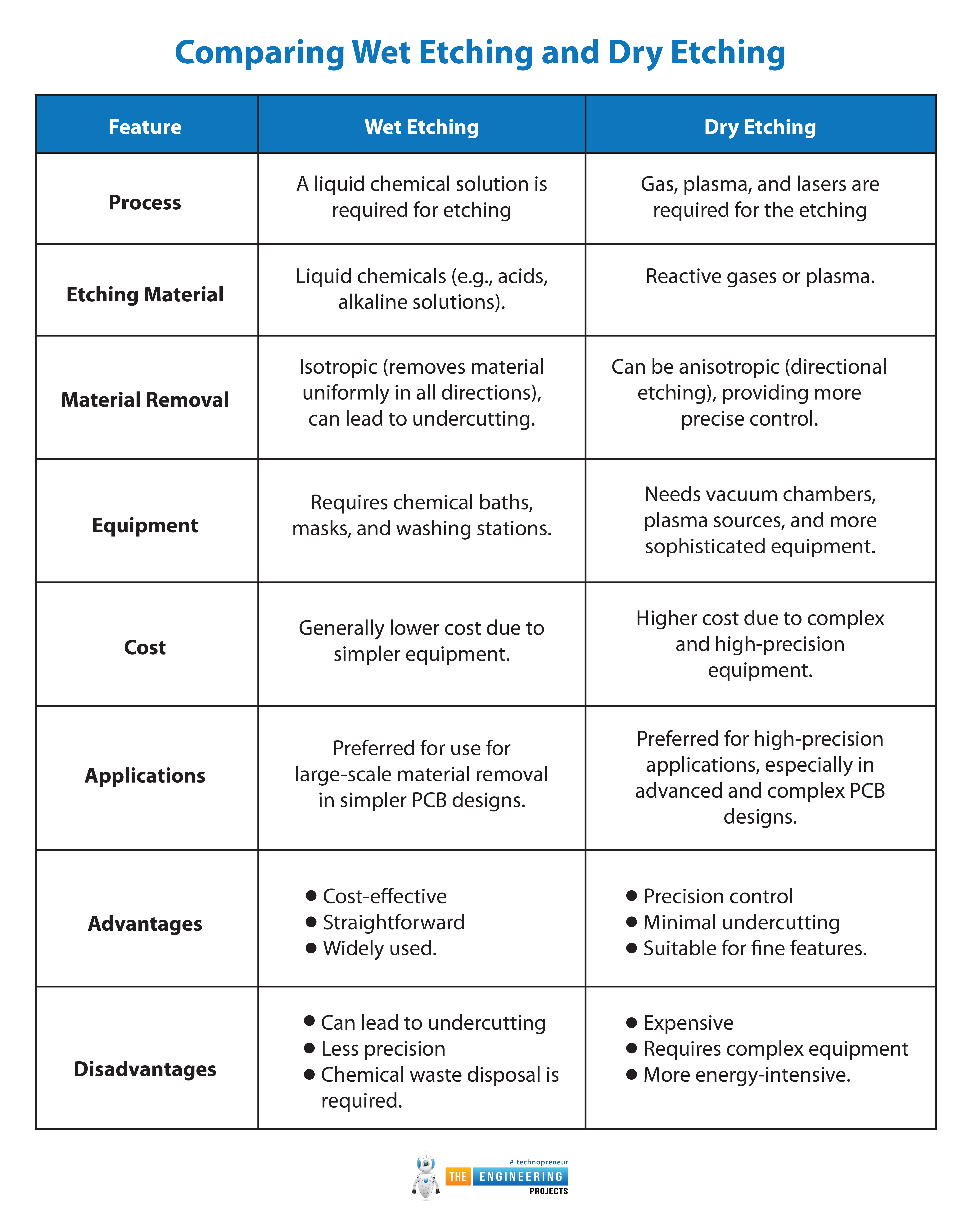
Feature |
Wet Etching |
Dry Etching |
Process |
A liquid chemical solution is required for etching |
Gas, plasma, and lasers are required for the etching |
Etching Material |
Liquid chemicals (e.g., acids, alkaline solutions). |
Reactive gases or plasma. |
Material Removal |
Isotropic (removes material uniformly in all directions), can lead to undercutting. |
Can be anisotropic (directional etching), providing more precise control. |
Equipment |
Requires chemical baths, masks, and washing stations. |
Needs vacuum chambers, plasma sources, and more sophisticated equipment. |
Cost |
Generally lower cost due to simpler equipment. |
Higher cost due to complex and high-precision equipment. |
Applications |
Preferred for use for large-scale material removal in simpler PCB designs. |
Preferred for high-precision applications, especially in advanced and complex PCB designs. |
Advantages |
|
|
Disadvantages |
|
|
Etching is one of the most basic steps in PCB manufacturing, in which the excess copper layer is removed from the PCB surface to get the desired circuit design. A copper layer is applied to the PCB, and, a mask of unreactive material is applied to the areas required on the board. The unneeded part is then allowed to react with the etchant and is dissolved. After that, the solvent is then removed and dried if required, and masking is then removed. As a result, sharp and fine designs are obtained. Etching is broadly classified into wet and dry etching. Examples of wet etching include alkaline and acetic etching, whereas dry etching includes plasma and laser etching. The choice of method depends on the board size, density, type of board, etc. Each method has its merits and demerits, and we have discussed all the basic points to clear up the topic.


