Factors Affecting the Prices of PCB Manufacturing & Assembly
A printed circuit board(PCB) is the most important part of an electronic device. A high-quality PCB is necessary to make a safe and durable device. PCB manufacturers should strive to maintain high quality at a low price. To achieve this goal, some matters should be taken into account.
Some key factors affect the prices of PCB manufacturing and assembly. PCB price depends on size, number of layers, quantity, etc. The material that we choose for PCB also affects the cost. The PCB printing process also matters in this regard. For example, some PCB manufacturers print PCBs manually while some control the whole process with CNC machines. Manual PCB printing is cheaper than CNC machine-printed PCBs. PCB manufacturing is a complicated task that needs experience and technology. A trusted PCB partner is essential for the electronics business.
Where to order cost-effective PCBs?
PCBX is an industry-leading PCB prototype manufacturer. Here you will get a One-Stop PCB Solution from Design to Mass Production.
PCBX specializes in providing 24-hour quick-turn PCB. We offer consistently low prices but high quality. We have 19 Years of Experience with proven expertise in prototype & production. Our Strict QC and advanced inspection ensure high reliability and stability. We have Advanced Automated Inspection (SPI, AOI, AXI) Services designed to ensure the utmost quality and consistency throughout the PCB production.
We integrate innovative technology including AI with efficient processes to deliver high-quality PCBs and complete product assemblies at competitive prices. This combination Minimizes rework and waste, saving on costs.
If you are looking for high quality at a low price, PCBX Fabrication House is the perfect place for you.
Following is a screenshot of the PCBx website’s home page.

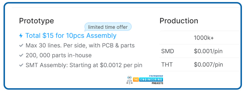
We have a special offer of $1 for 10 PCB prototyping, and $15 for 10 PCB Assembly, without compromising on quality. We also give free PCB assembly coupons. You can see the offer on our website as shown in the following picture.
In this article, we will discuss the Factors Affecting the Prices of PCB Manufacturing & Assembly. We will also try to find a balance between cost and quality.
Delivery time
How does shorter delivery time increase manufacturing costs?
Delivery time plays an important role in the manufacturing cost of PCBs. Urgent or express delivery adds more to the cost. When the customer demands urgent delivery, the manufacturer needs to employ extra labour. Workers may need to do overtime. Additional machineries are put into operation. These will increase the overall manufacturing cost.
Due to shorter delivery time requirements, manufacturers often need to adjust production schedules and processes to ensure timely order completion. They may need to rearrange production lines, prioritise urgent orders and accelerate production speed. As a result, costs associated with production adjustments are increased.
After manufacturing the PCB, then comes the question of delivery. Urgent delivery needs special arrangements. Air freights and express delivery services add more to the cost.
PCBX offers a flexible assembly time frame. It can range from as little as 24 hours to a few weeks. You can select the time option that best suits your schedule and budget. We want to ensure transparency. This is why our turn-time policy begins once all the necessary components are ready and all the required PCB files are complete for our assembly work. These files include Gerber files or other PCB file formats, Centroi(PNP file), BOM, and any other essential data, documents, images, or photos. This approach accounts for the complexity involved in determining the turnaround time for PCBA services.
Complexity of design
The design plays an important role in the manufacturing cost of a PCB. The more complex the design is, the costlier it becomes. Complex design usually means the components are densely placed and a lot of traces and vias are very close to each other. This type of complex PCB needs extra care during manufacturing. Complex circuit boards may require larger board areas. The number of layers may also increase. All of these factors will eventually increase the production cost of the PCB. So, it is wise to keep the design as minimalistic as possible. If the whole circuit can be accommodated in a single-layer board, there is no point in making it double-layered. Traces should be placed cunningly to save more place.
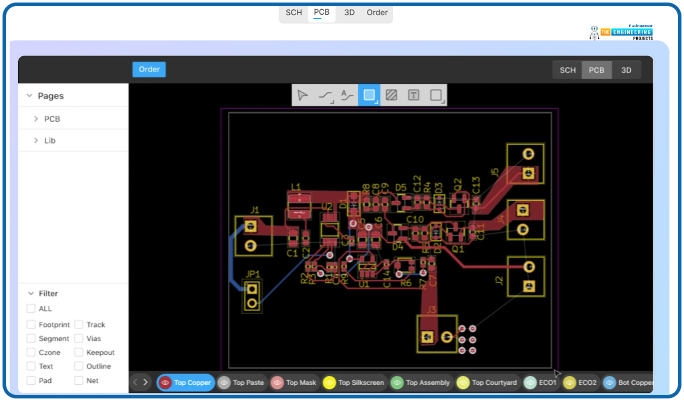
We want to make your PCB designing task easier. We have the PCBX designer to help you with the design. It is an online PCB designing platform. It is quite easy to learn. It takes not more than 5 minutes to learn this tool. No matter what device you use, you can always run this tool. You can import circuit files from other PCB Designer software into PCBX for viewing, editing, and modifications. Following is what the PCBX designer looks like.
PCB Size
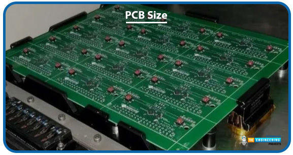
Bigger PCBs usually need more substrate materials. They also need more copper foil. All of these materials increase the cost. For high-density boards, the increase in material costs can be significant.
Larger PCBs may need a series of complex manufacturing processes. They depend on larger production equipment, such as larger cutting machines, and larger copper plating holes or slots. This increases manufacturing complexity and costs. The following picture shows a PCB which is bigger than usual.
PCB shapes
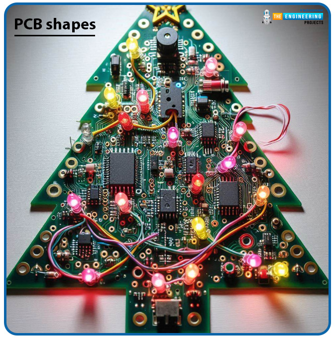
PCBs are usually rectangular. But often they are of other shapes. Such as round PCB, Christmas tree-shaped PCB etc. To cut circuit boards in unusual shapes, additional processing steps or customized processes may be required, further adding to manufacturing costs. The following picture shows a PCB having an exotic shape.
Larger PCBs may lead to higher shipping costs. Due to their larger size, they need larger packaging boxes or additional protective measures to ensure the safe transportation of the products. Transportation of big-size PCBs may pose some challenges. As a result, PCB suppliers may need to pay additional charges, such as oversize cargo fees or higher shipping costs.
Number of layers
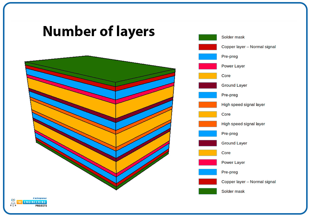
An increase in the number of layers means the consumption of substrate materials, copper foil, insulation materials, etc., also increases. Thus the number of increased layers raises material costs. The following picture shows the standard composition of a multilayer PCB.
Multi-layer PCBs need a more complex manufacturing process. In multi-layer PCBs, additional processing steps may be required. These steps include lamination of copper foil layers, drilling, and alignment of inner layer circuitry. These processes add to the complexity and difficulty of manufacturing, consequently increasing manufacturing costs.
PCBs must ensure stable signal transmission. This is why multi-layer PCBs require precise alignment and connection between each layer. Multi-layer PCBs have vias between layers to interconnect the components of each different layer. Electroplated vias are very common in these PCBs. To accommodate all these features, multi-layer PCBs demand higher levels of manufacturing technology and equipment. This also contributes to higher manufacturing costs.
With the help of modern technology and expertise, PCBX is capable of manufacturing multi-layer PCBs consisting of up to 8 layers.
Substrate Material
Different types of substrate materials have different prices. The substrate material you choose directly manipulates the price of your PCB.
For example, commonly used FR-4 fibreglass composite materials are typically cheaper than high-frequency materials like PTFE. The following figure depicts the placement of substrate material in PCBs.
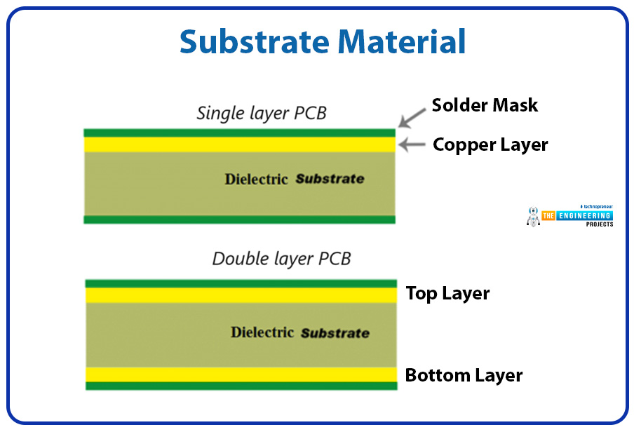
There are certain special applications of PCBs. Many PCBs need to operate in high-frequency, high-speed, or high-temperature environments. For this purpose, special substrate materials may be required to meet performance requirements. Generally, these special substrate materials are more expensive.
The price of PCB directly depends on the thickness of substrate materials. There are some commonly used high-frequency substrate materials with relatively high prices. RO4350, RO5880, etc. are mentionable among those.
Trace Width and Spacing
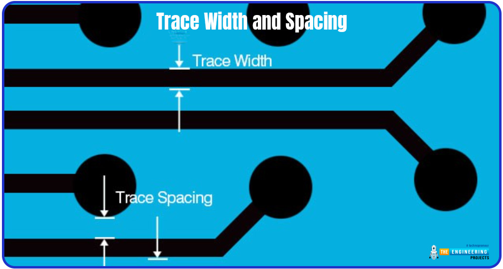
Finer manufacturing methods and higher-end production equipment are needed for smaller trace widths and spacings. Reduced trace widths and spacings may require the employment of more sophisticated lithography methods and drilling tools, which raises the cost of production. Smaller trace widths and spacings could also result in more complicated production processes and longer processing times, which would raise manufacturing prices even more.
Reduced Yield Loss
During the manufacturing process, smaller trace widths and spacings may result in a greater yield loss. There might be more scrap or faults during production as a result of the reduced trace widths and spacings, which would raise production costs and reduce yield. Smaller trace widths and spacings may also raise the failure rate during manufacturing, necessitating the need for additional steps to lower scrap rates, such as stepping up inspections or changing production procedures, which raises the cost of manufacturing.
The following picture shows trace width and trace spacing.
Drill holes
Increased Processing Costs
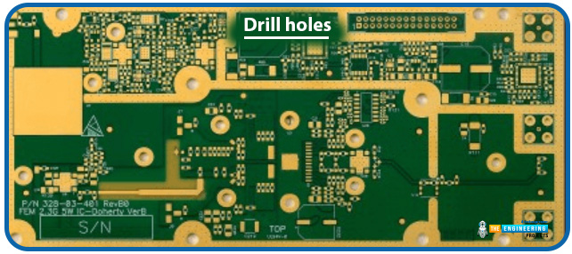
Another thing that heavily influences the price of your PCB is the number and size of drill holes. Smaller drill holes need smaller-sized drill bits. It increases the processing cost of PCBs. There may be some specialized PCB requirements, such as blind vias, buried vias, or controlled-depth holes. Special drilling processes are often required to meet these demands. These special drilling processes typically require higher-level processing equipment and more complex operational steps, thus giving rise to processing costs.
The following picture shows a PCB with different sizes of drill holes.
Increased Material Loss
Drilling processes sometimes lead to material loss. Increased material loss rates result from more material being removed and sliced away when there are more drill holes. Furthermore, additional drill holes might be needed for some specific PCBs, such as high-density boards, in order to achieve complicated circuit layouts, which would further increase material loss rates. To meet specific PCB criteria, including blind vias, buried vias, or controlled-depth holes, unique drilling techniques could be required. Processing expenses are increased because these unique processes usually call for more sophisticated operational procedures and sophisticated processing equipment.
Higher Loss of Materials
Material loss can occur during drilling operations. Increased material loss rates result from more material being removed and sliced away when there are more drill holes.
Surface Treatment
copper is oxidized and deteriorates in the presence of air. Oxidization seriously affects the electrical properties and solderability of PCBs. The implementation of PCB surface treatment is important for the improvement of the reliability and shelf life of PCBs. The quality of metal-to-metal joints depends on surface treatment These treatments also contribute to the higher manufacturing cost of PCBs.
There are 8 kinds of PCB surface treatment methods. These are-
HASL, hot air solder levelling
OSP, Organic coating.
ENIG.Chemical gold.
IAG. Immersion Silver.
ISN. Immersion tin.
Electroplated Nickel Gold.
Electroless Palladium.
ENEPIG, Electroless Nickel Electroless Palladium Immersion Gold.
The following picture shows different PCB surface finishes.
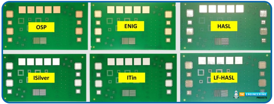
The costs of all these surface treatment techniques are not the same. For example, organic coating is cheap. On the other hand, palladium is a valuable metal. So, the Electroless Palladium process is expensive. Expiration dates of various surface treatments are different. You have to select the surface treatment according to your application.
How can you decrease PCB manufacturing costs?
Here are some tips to follow if you want to cut down on the manufacturing cost of PCBs
Right placement of components
Component placement of PCB should be done in such a way, that you can connect them to each other by the shortest possible path. When you convert a schematic to a PCB layout, please pay attention to the components that are connected to each other. Place the connectable components close to each other. Try to keep the traces as short as possible.
Aim for the lowest number of layers possible
PCB cost increases proportionally with the number of layers. So, try to accommodate all the traces, vias and components in the lowest number of layers possible.
Remove unnecessary trace spacing
It is essential to maintain an optimum distance between the traces to avoid DRC errors. However, traces should not be placed so far from each other that the total board area becomes cumbersome. Try to place the traces as close as possible to each other without violating DRC rules.
Follow DFM guidelines
DFM stands for design for manufacturability. DFM guideline is a set of rules for cost-effective and efficient manufacturing. By following this guideline, you can optimize the sizes, materials and tolerances of PCBs to reduce costs.


