Common Issues Faced in PCB Designing

PCB stands for printed circuit board. You will find PCBs in pretty much all electronic devices. It is usually green/blue in color. The PCB is a circuit in a board that permanently holds all the components of a circuit. It is the main part of an electronic device. This board controls and regulates the function of the whole device. A circuit may work perfectly in a breadboard. But breadboard circuits are not suitable for use. It will only be eligible to be used in a ready-made product if implemented in a PCB. This is why PCB designing should be done with utmost care.
Where to order error-free PCBs
It takes a lot of knowledge and expertise to manufacture good-quality PCBs. PCBway is a trusted PCB manufacturer. While their head office is located in China, they ship PCBs worldwide. The following image shows the home page of PCBway.

PCBway Fabrication House is the best PCB manufacturer for professionals and hobbyists. There you can not only print your PCBs. You can get consultancy regarding the whole manufacturing process. Together with a top-notch design and an expert manufacturer, you can produce a high-quality and durable PCB. The following pictures shows how the order page of PCBway looks.

PCB design should be an accurate process. It involves several critical steps. Different challenges may arise in each step of this process. It is important to detect and solve these problems at the early stage of manufacturing the product. Otherwise, we cannot guarantee a reliable electronic gadget. This article discusses the common problems faced in PCB designing and practical solutions to solve these.
Misplaced components
Problem
This problem often occurs when the designer is a newbie. The wrong placement of components causes some problems. Due to this mistake, the size of the PCB increases unnecessarily. That costs unnecessary money. Soldering becomes difficult if the components are haphazard. Electromagnetic interference (EMI) may also occur and overall signal integrity may also be affected. Misplaced components also result in the following problems:
- Difficulties in soldering during the manufacturing process
- Electromagnetic interference (EMI)
- Signal integrity issues.
Solution:
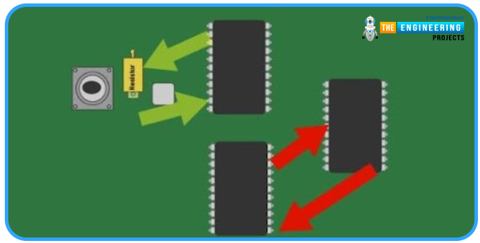
We should place components in a PCB wisely. The components should be arranged in such a way that the traces will be as short as possible. The components that are supposed to be directly connected, must be placed close to each other. The following image shows a decent arrangement of components in a PCB.
90-degree traces
Problem:
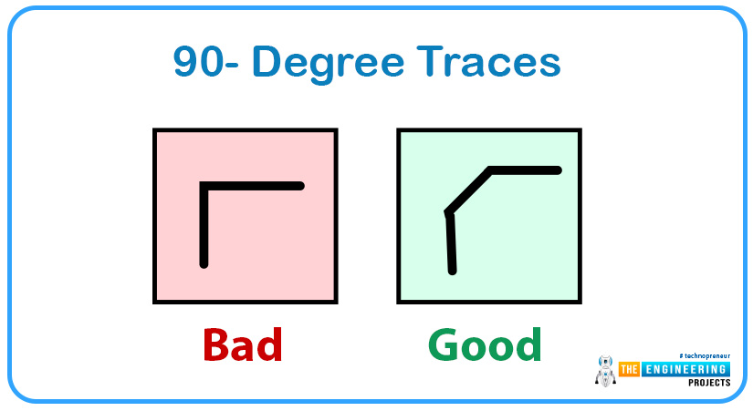
Making 90-degree traces is a big no-no for pro-level PCB designs. The sharp edge created by this type of tracing creates extra stress on the traces. These traces are more likely to crack or break. The life span of such badly designed PCBs is less than usual. The corners of a right-angled PCB have higher electric field density than standard ones.
Right-angle PCB traces affect signal integrity. The effect of a PCB trace's right-angled corner is the same as that of a transmission line coupled to a capacitive load. This is called parasitic capacitance. As a result, the transmission line signal's rising time is slowed down.
Solution:
Designers should always avoid right-angled traces. In PCB designing software like Proteus, there are functions for making curved traces. We must use those to make our traces curved and not susceptible to cracks after long-term use. The following image shows the difference between a bad and a good trace.
Poor Signal Integrity
Problem:
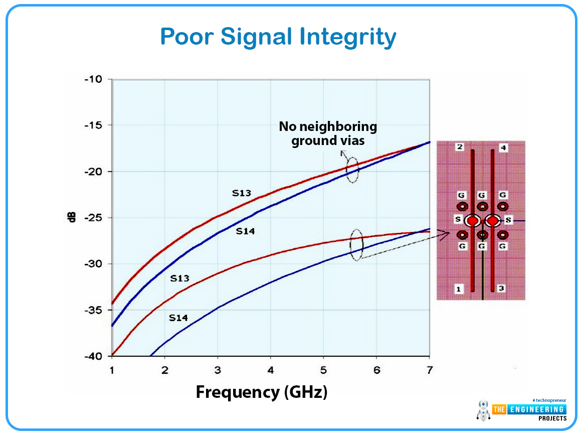
PCB designers must ensure signal integrity. Signal transmitting across the PCB should not distort. Poor signal Integrity is caused mostly by wrongly designed traces, crosstalk, impedance mismatch etc. Signal distortion causes transmission errors.
Solution:
Modern PCB designing platforms have many important tools that help PCB designers maintain good signal integrity. By knowing how to use them properly, you can avoid errors like uncontrolled line impedances, propagation delays and signal attenuation.
The following figure shows a relationship between coupling traces and SI(signal integrity parameters.)
Electromagnetic Interference (EMI)
Problem:
EMI causes noise and signal interference. Noise degrades the performance of a PCB. EMI increases with frequency. This may cause many problems in high-frequency circuits and designs where components are congested.
Solution:
EMI can be handled with a combination of design strategies. One method is to use ground planes. We have to place ground planes in such a way that they absorb and redirect electromagnetic emissions. It is also possible to reduce EMI by reducing the current loop area.
It is also important to Shield critical components and traces. Additionally, careful routing of high-frequency traces away from sensitive analog signals can minimize interference.
Heat is generated in PCBs in several ways. Some prime sources of heat generation in PCBs are the active devices or chips that generate heat. Another source is created when an RF power is applied to the circuit. In the case of a double-layered PCB, the copper has extremely high thermal conductivity. On the other hand, the substrate is a thermal insulator that has a very low conductivity. A good-quality PCB must Have a high heat flow. There must be sufficient heat sinks around active components. It is important for keeping the circuit cooler by more efficient heat transfer from the heat source to the heat sink.
The following picture shows some EMI shielding films.

Power Distribution Problems
Problem:
Structurally a PCB can be perfectly alright. Still, it will be useless if the power supply is not adequate. Power distribution should be according to the requirements of each and every component. There may be different voltage and current requirements for different components of a PCB. For example, a PCB may consist of a microcontroller that operates at 5V, but there may be a motor driver that operates at a different voltage level. So, different amounts of voltage and current must be supplied to different parts of the circuit. It is necessary to design a reliable power distribution network. There are PDN analyzers that can detect anomalies in the PDN.
DRC error
Problem:
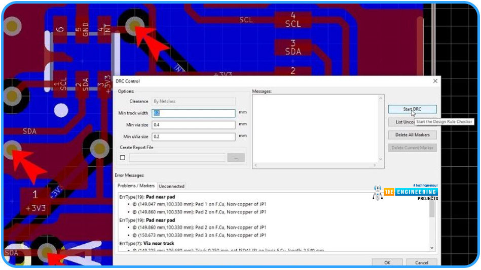
If you know how to use a PCB designing software, you already know this term. DRC stands for Design rule check. DRC error occurs when you do not maintain the minimum trace-to-trace distance defined by the software. For example, the minimum spacing between two traces of a 2-layered PCB is 6 mils (mil=1/1000 inch). If any two traces of your PCB layout are closer than this, the software will show a DRC error. The same error messages will appear also when-
Traces are overlapped with each other
The power plane and the GND plane touch one another
The minimum standard distance between a trace and an adjacent via is not maintained.
We should never ignore DRC errors. If we print a PCB without solving DRC errors, chances are high that it will blow away after powering up.
Solution:
There should be no DRC error in the PCB layout. Each DRC error detected by the software should be corrected before printing the PCB. You have to edit your design to meet the requirements of the software. You may need to adjust the sizes of the traces and vias to comply with the rules. The following image shows the DRC tool of a PCB designing software.
Manufacturing Defects
Problem:
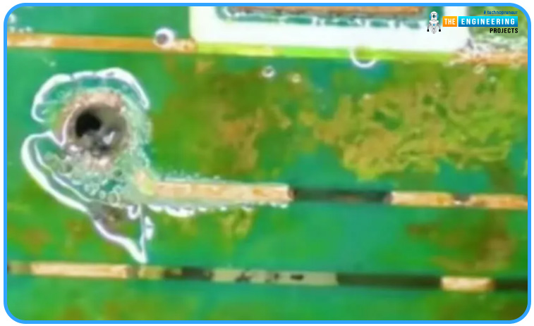
You may design a flawless PCB, but manufacturing errors can still occur. You can see many short circuits and broken traces. Sometimes it becomes also impossible to read the texts written on the silkscreen. The following picture shows a broken PCB trace.
Solution:
A good collaboration with the manufacturer may help you solve these manufacturing defects. The customer should provide clear and detailed documentation. It is essential to include the fabrication drawings and assembly instructions. It is helpful to perform a manufacturability (DFM) check to identify potential issues before production. Automated optical inspection (AOI) and in-circuit testing (ICT) during manufacturing can also find defects early.
Grounding Issues
Problem:
A well-designed ground system is required for Modern high-speed electronics. PCBS need to operate at their best performance. If the PCB ground is not properly implemented, the circuit board may experience many different problems with noise and electromagnetic interference (EMI).
Sometimes the ground net in a PCB design can appear confusing. Yes, there are many connections, but since most designs will have one or more ground planes in their layer stacked up, you just add a via to the ground, and the work is done. Right? Theoretically, that is correct, practically, there are lots more that need to go into your PCB grounding technique to build a good power delivery network.
Solution:
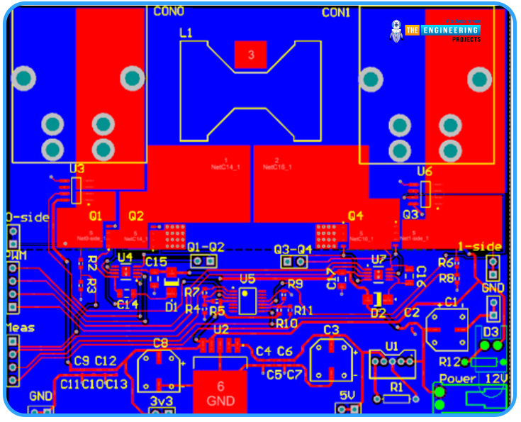
A single, continuous ground plane is typically the best approach for minimizing ground loops. The following image shows a PCB layout with properly designed POWER and GND planes.
Soldering Issues
Problem:
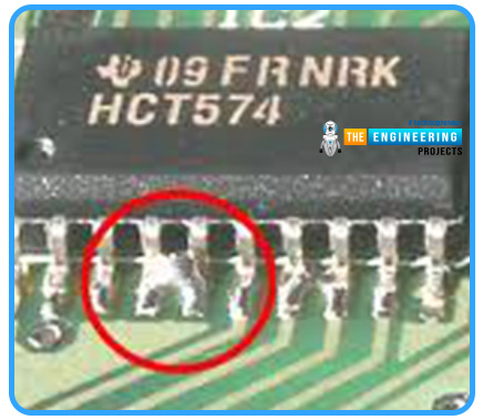
Soldering issues such as cold joints, bridging, and insufficient solder can lead to unreliable connections and component failures.
The following image shows an example of an accidental short circuit.
Solution:
Designing with manufacturability in mind can help prevent soldering issues. Ensuring appropriate pad sizes and clearances for components can facilitate proper soldering. Specifying the correct solder mask and paste layers in the design files is also important. Automated soldering processes, such as reflow soldering, should be used whenever possible to ensure consistent and reliable solder joints. Inspecting solder joints using AOI and X-ray inspection can catch defects before final assembly.
Inadequate Clearance
Problem:
Inadequate clearance between traces, pads, and components can lead to shorts and an increased risk of crosstalk, affecting the PCB's reliability and performance.
Solution:
Following the clearance guidelines provided by the PCB manufacturer is essential. Maintaining adequate spacing between traces and pads can prevent shorts and crosstalk. Using the DRC tool in the CAD software to check for clearance violations can help identify and rectify issues before fabrication. Also, consider the voltage levels and environmental factors like humidity and temperature. It can guide appropriate clearance settings.
Multilayer Design Complications
Problem:
Designing multilayer PCBs introduces complexity, such as ensuring proper layer stack-up, signal routing, and maintaining signal integrity across layers.
Solution:
Planning the layer stack-up early in the design phase is critical for multilayer PCBs. Assigning specific layers for power, ground, and signal routing can help manage complexity. Using blind and buried vias can optimize space and routing options. Ensuring proper alignment of vias and traces across layers is essential for maintaining signal integrity. Simulation tools can assist in verifying the performance of multilayer designs and identifying potential issues.
Failure to Consider Manufacturing Tolerances
Problem:
Tolerance means the maximum deviation from the design at the time of the manufacturing process. There are always big differences between theory and practice. Your design may be perfect in your software, but you have to consider manufacturing tolerances in practice. If we do not take it into account, our PCB may fail.
Solution:
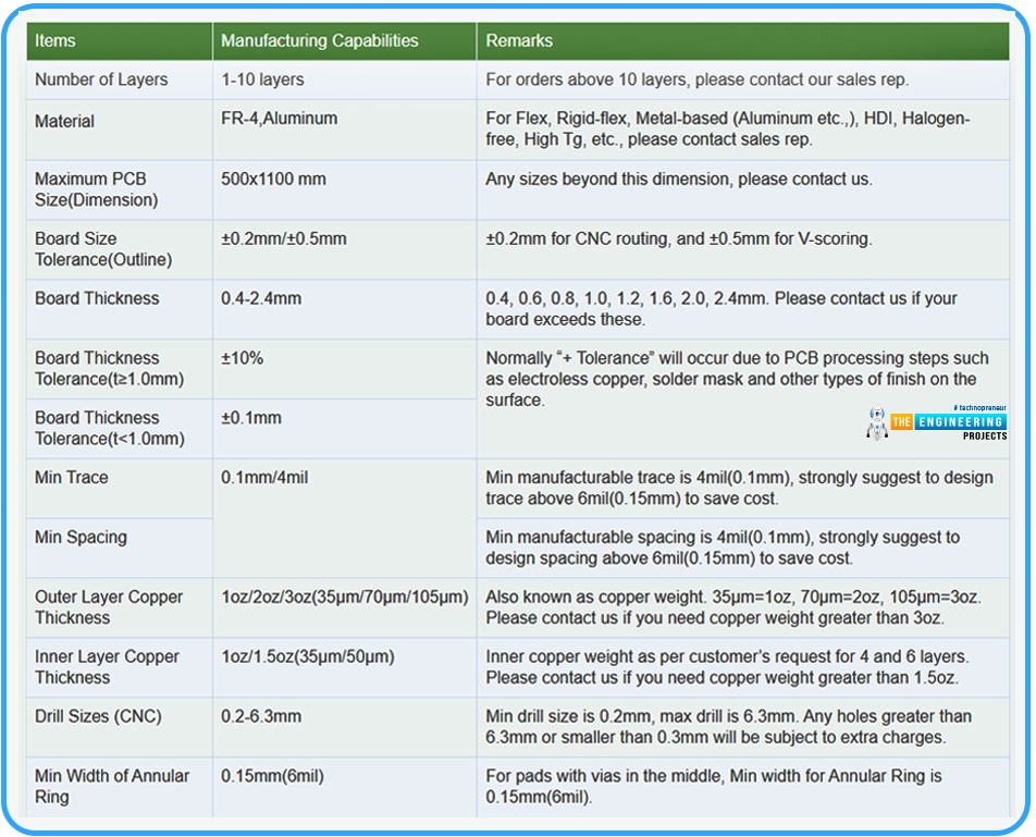
It is best to check the manufacturing tolerances of the PCB manufacturing company. The following image represents PCBway’s manufacturing tolerance guideline. To learn more about PCBway's manufacturing tolerance policy, you can click here.
Environmental Factors
Problem:
While designing a PCB, it is necessary to take environmental factors into account. You must consider the temperature, humidity, and atmospheric pressure of the environment where it is likely to be used. For example, a PCB designed for an industrial purpose should be more robust than a PCB of a home appliance. PCBs are likely to damage early if they are not compatible with their surroundings.
Solution:
First of all, we have to select the components according to their specifications and operating temperatures. For industrial products, all components and the board itself should be industrial-graded. For better heat dissipation, use thermal vias, heat sinks etc.
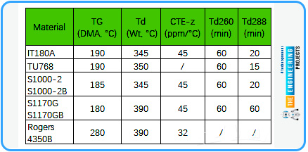
Following is a chart of high TG materials used by PCBway.
Conclusion
PCB manufacturing is a process that needs a lot of scrutinization, time and dedication. PCBs are often printed on a trial-and-error basis. It should be our goal to save as much money and time as possible while not compromising the PCB quality. We should correct all DRC errors before printing a PCB. We need to provide a proper thermal management system, and proper shielding for removing signal interference. We should not tend to make the design on an ad-hoc basis. Rather, we must always try to make a durable PCB. We should choose a dependable manufacturer.


