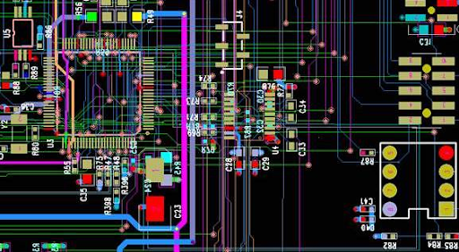

Introduction to Microwave PCB


Hello, peep! I hope you are doing great. Today, I’ll explain to you a very basic and interesting topic in the electrical world. We know printed circuit boards act as the backbone of complex circuits, and microwave PCBs are an important member of this family. These are the integral components of the high-frequency circuit designs. We will study microwave PCBs in detail and find out the perfect type of circuit where these are widely used.
Now, the question arises as to where the best PCBs can easily be ordered. It is crucial to get sensitive devices like printed circuit boards from the right vendor because quality is the first parameter to be considered in such shopping. One of the most reliable sources to get microwave PCBs without any difficulty is PCBWay Fabrication House. It is a popular manufacturer and seller of PCBs and their prototyping. The users can have low-volume production and a wide variety of PCB assembly services, all of which are available under one roof.

PCBWay is one of the largest manufacturers of PCBs and provides a great variety of PCBs and related components. They not only sell PCBs but also provide services such as manufacturing, designing, prototyping, and other processes. They have a large staff that helps the users to get their queries solved instantly. I suggest you visit PCBWay.com to get any services related to electronic circuit components, especially PCBs.

In this article, we’ll start learning the introduction to microwave PCBs through the basic definition. After that, we’ll understand the features in detail and see the basic applications in different sensitive domains of electronics to understand their scope. Here is the introduction of these PCBs.
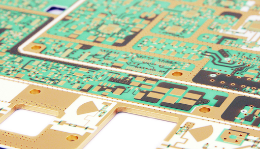
Introduction to Microwave PCB
Microwave printed circuit boards are a specialized category of PCBs that are designed to be operated according to the stringent requirements of high-frequency circuits. As the name suggests, the basic purpose of using these PCBs is to have the best performance at a higher level of frequency, even in microwaves where other PCBs do not provide the right performance. At such high frequencies, these PCBs show the best performance with minimal loss and distortion. This is the reason why these have applications in extraordinary fields such as aerospace, medical devices, etc.
The basic reason behind the best performance of this PCB is because of its design. From material selection to the fabrication process, these PCBs are designed to keep high frequency in mind. Hence, the nuances of the material are vital to achieving signal integrity with reliable output.
Features of Microwave PCBs
Microwave PCBs are different from traditional PCBs because they are designed for the extraordinary Understanding the features of microwave PCBs will help you a lot to know their basics and applications.
Microwave PCB Material
As mentioned before, the basic reason behind the robust performance of these PCBs is because of the material used in their production. These are made with specialized substrate materials that have low dielectric constants and low dissipation factors. Common materials used in their production are:
Polytetrafluoroethylene (PTFE)
FR-4 with PTFE
Ceramic-filled PTFE composites
Here, the basic material is PTFE, whereas FR- and ceramic-filed PTFE are its variants.
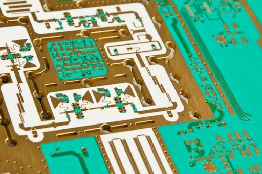
Microwave PCB’s Copper Thickness
As compared to ordinary PCBs, microwave PCBs are employed with thicker copper layers. This not only reduces conductor loss but also contributes to better thermal management. For this, more material is required, and usually, the thickness of microwave PCBs is greater than that of many other types.
Microwave PCBs Control Impedance
One of the most critical features of microwave PCBs is their impedance maintenance. They are designed in such a way that they prevent the phenomenon of signal reflection in microwave signals. Microstrip or stripline configurations are important techniques used during its design, and this ensures efficient power transfer from one point to another in the PCB.
Microwave PCB’s Isolation and Crosstalk
An important feature of this PC is that, during the design process, great care is taken to isolate the component. This includes processes such as strategic component placement and optimized routing so that the circuit has minimal crosstalk.
Microwave PCB’s Via Design
Another reason why these PCBs provide the best signal integrity is the via design. The following table shows the via design options in the microwave PCBs:
Feature |
Through-hole Via |
Blind Via |
Buried Via |
Connection |
Extends through the entire PCB |
Connects an outer layer to one or more inner layers |
Connects inner layers without penetrating the outer layers |
Visibility |
Visible on both the top and bottom of the PCB |
Visible on one side of the PCB (typically the top) |
Not visible on either side of the PCB |
Manufacturing method |
Drilling through the entire PCB |
Drilling partway through the PCB, then plating the remaining portion |
Laser drilling or plating through micro vias |
Cost |
Less expensive |
More expensive than through-hole vias, less expensive than buried vias |
Most expensive |
Reliability |
Highly reliable |
Less reliable than through-hole vias, more reliable than buried vias |
Least reliable |
Applications |
High-current applications, high-density designs |
Applications where vias need to be hidden on one side of the PCB, such as for cosmetic reasons or to prevent EMI |
High-density designs, applications where vias need to be hidden on both sides of the PCB |
Microwave PCB’s EMI/EMC Compliance
Another way to maintain the performance of these PCBs is to set the electromagnetic interference (EMI) and electromagnetic compatibility (EMC) compliance in the design. This helps a circuit to adhere to the regulation of electromagnetic standards so that every component in the circuit has the experience of the right EMI and EMC. This not only results in better circuit design but is useful in testing and validation.
Microwave PCB’s Applications
As we have discussed so far in this article, microwave PCBs are a specialized type of PCB. these have applications in the areas where PCB tolerance and high sensitivity are required. Here are some major fields where these PCBs are used:

Microspace PCBs in Aerospace and Defence
In areas like aerospace and defence, high-performance circuits are extensively used and reliability is an important factor of these circuits. Here, the microwave PCBs are considered one of the best choices. The two most critical applications are discussed below:
For military and aerospace applications, radar systems are the basic devices and these require accurate performance all the time. In these devices, microwave PCBs help to get precise and rapid signal processing.
The electronic warfare system circuity requires a base that may bear the high frequency easily. For such systems, the microwave PCBs are the best choice. As a result, these PCBs help to have the best performance.
Microspace PCBs in Telecommunication Systems
The microwave PCBs are the integral base of the systems in the telecommunication fields. These systems are loaded with wireless communication devices and here, usually, the best frequency is in the form of microwaves. Therefore, most of the devices use microwave PCBs to get the best performance.
Communication with the satellite requires a high frequency to communicate through the distance. For this, reliable devices that can bear the high frequency without disturbing the output are required and this is possible with the microwave PCBs.
Mircospace PCBs in Medical Devices
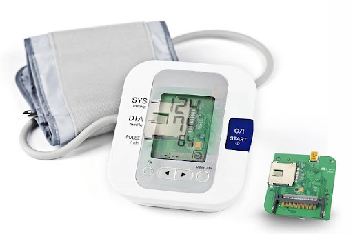
The sensitive areas like medical imaging devices where accuracy and precision are the life-saving parameters, are always the best pieces of equipment used and microspace PCBs are worth discussing as part of these devices. Here are some medical applications where these PCBs are used:
In medical imaging devices, accuracy is an important factor because of the limitations of the colours. Here, the base of these devices is the microwave PCBs, because ideally, these do not distort the output even at the high frequency. Two important applications in this regard are magnetic resonance imaging (MRI) and computed tomography (CT) scanners.
These PCBs have applications in radio frequency (RF) ablation systems, where they help the expert work on medical treatment with precise control.
Microwave PCBs in Research and Scientific Instruments
In laboratories and scientific research departments where heavy calculations are required and the device runs continuously for a long time, it is better to use microwave PCBs because of their feature to bear high frequencies.
The research applications get the most benefit from these PCBs and can work with the best results from their long-term calculations.
The scope of microwave PCBs is not limited to these fields but is widely used in industrial automation, consumer electronics, etc.
So, in this article, we have understood the basics of microwave PCBs. We started with the basic introduction and understood the features to clarify the concepts. After that, we saw the applications of microwave PCBs in different sensitive areas where they are used because of their features like accuracy and precision. Moreover, in the beginning, we discussed how PCBWay is the best choice to buy microwave PCBs. I hope you liked the content, and if you want to know something more, you can contact me through the comment section.


 1 user


 Continue Wishlist


 Getting Started Guide
 Help Center
 Contact us
 Doist Blog
 Privacy
 Security
 Terms of Service
 What's new: Channel Descriptions


 Printed Circuit Boards
 xeohacker
 0 Comments


 Introduction to Microwave PCB
Microwave PCB
Microwave PCB applications
Microwave PCB manufacturing
 Sunday, February 4, 2024


