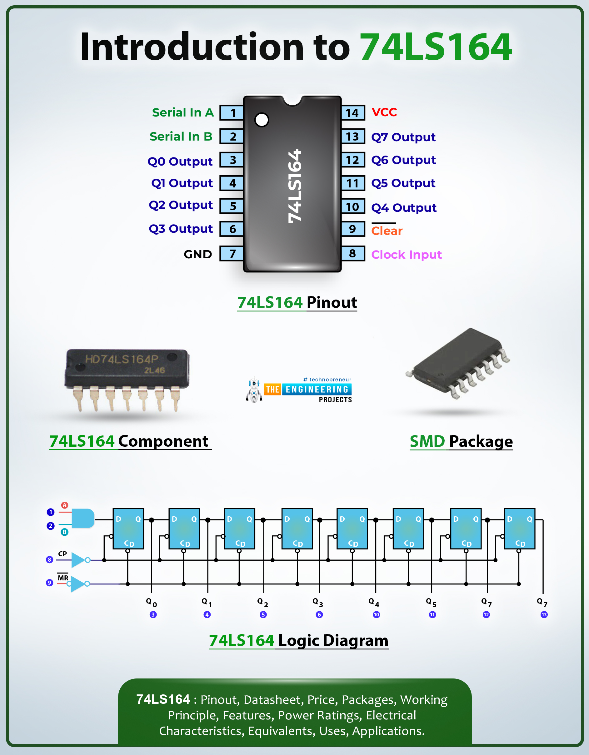
Hi pupils! Welcome to another article on integrated circuits. We have been studying different ICs in detail and today the topic is 74LS164. It is another important family member of the 74xx series of ICs and is widely used in different types of digital devices because it is a serial-in parallel-out shift register.
In this article, we’ll discuss the 74LS154 in detail. We’ll start with the introduction and after that, I’ll share a detailed datasheet with you that will help you understand the workings and basic structure of this app. After that, I’ll discuss the working principle and share a simple project of this IC in proteus. Moreover, I'll share the measurement of the dimensions of this IC and in the end, there will be the details of applications for 74LS164. This article has all the basic information about this IC and let’s start our discussion with its introduction
74LS164 Introduction
It is a synchronous reset register that takes the serial input but can process and represent the data in the parallel output.
It belongs to the 74LS family; therefore, it is a low-power Schottky TTL logic circuit.
It has an asynchronous clear.
It is a 14-pin dual inline package (DIP) and sometimes the package is a small outline integrated circuit (SOIC).
It acts differently in the situation. At the low logic level, it follows the logic given next:
It may inhibit the entry of new data
At the next clock pulse, it resets the flip-flops to the low level
As a result, it has complete control over the incoming data.
At the high logic level, any input enables other inputs and this determines the start of the first flip-flop.
This is one of the most simple and versatile registers; therefore, it has multiple applications in different fields where digital circuits are used.
74LS164 Datasheet
The information about the datasheet of this IC will help you understand the basic information in detail.

74LS164 Connection Diagram
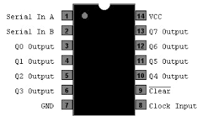
The 14-pin package has a specific pin configuration. Each PIN has a specific name according to its function. This can be understood with the following connection diagram
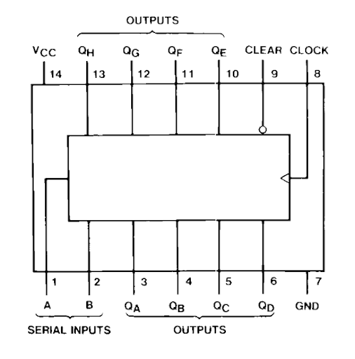
It has the outputs on both sides of the IC.
A cut on the ground pin side indicates the right direction of the pin combination.
It has two serial inputs.
74LS164 Pinout Configuration
The details of the above diagram will be clear with the help of the following table:
Pin No |
Pin Name |
Description |
1 |
A |
Data Input |
2 |
B |
Data Input |
3 |
Q0 |
Output pin |
4 |
Q1 |
Output pin |
5 |
Q2 |
Output pin |
6 |
Q3 |
Output pin |
7 |
GND |
Ground Pin |
8 |
CP |
Clock Pulse Input |
9 |
MR’ |
Active Low Master Reset |
10 |
Q4 |
Output pin |
11 |
Q5 |
Output pin |
12 |
Q6 |
Output pin |
13 |
Q7 |
Output pin |
14 |
Vcc |
Chip Supply Voltage |
Table 1: 74LS164 pinout configuration
74LS164 Sequential Logic Circuit Operations
The combination of the inputs in this IC results in different conditions. Here is the detailed table for this:
CP |
DSM |
MR |
Operation |
Description |
Additional Notes |
↓ |
X |
X |
Clear (Asynchronous Master Reset) |
It immediately clears all flip-flops to 0, regardless of clock or other inputs. |
Overrides all other operations. |
↑ |
X |
H |
Hold (No Change) |
Maintains the current state of the register. |
It is useful for pausing data transfer or holding a specific value. |
↑ |
L |
X |
Load Parallel Data |
Loads the parallel data inputs (A-H) into the register. |
It occurs on the next rising clock edge. |
↑ |
H |
H |
Shift Right (Serial Input) |
Shifts data one position to the right, with new data entering at the serial input (SER). |
Occurs on each rising clock edge. |
Table 2: 74LS164 Sequential Logic Circuit Combination
This can be understood with the following information:
CP (Clock Pulse) = It controls the timing of data transfer and operations.
DSM (Data Strobe Master) = It enables parallel data loading when low.
MR (Master Reset)= It asynchronously clears the register when low.
X = It is the "don't care" condition, which means the input can be either high or low without affecting the operation.
↑ = It represents a rising clock edge.
↓= It represents a falling clock edge.
74LS164 Logic Diagram
The internal structure of any IC is much more complex than the connection diagram because ICs consist of a combination of different logic gates. Here is the logic diagram that displays the internal structure of the 74LS164:

Figure 3: 74LS164 Logic Diagram
Here, you can see how the basic logic gates combine to form the 74LS164.
74LS164 Timing Diagram
The operations and the clock shifting of the 74LS164 are understood with the following diagram.
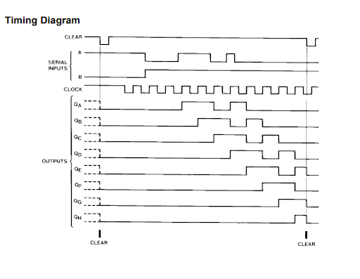
Figure 4: 75LS164 Timing Diagram
This is a general representation of the timing diagram that can be understood with the help of the following points:
The rising edge clock pulse signal (CP) results in the shifting operation of the pulse.
When the parallel load phase is applied to the parallel inputs, it affects the content of the shift register.
The master reset signal clears the active low transition and clears the shift register asynchronously.
If you want to know more details about the datasheet for 74LS164, then you can visit this:
74LS164 Circuit Diagram
The general representation of the circuit diagram is important to understand when you are using it in practical work. Here is the diagram that clearly specifies the working and pin connections of this IC.
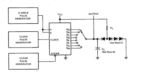
Figure 5: Circuit diagram of 74LS164
74LS164 Working Principle
The 74LS164 has a pin named MR, which is a low active input master reset pin. The output of this pin remains in a low state until the state of the circuit is low. In such conditions, the values on the input do not affect its state.
The MR pin is also referred to as the reset or clear mode pin.
The procedure of the circuit’s working is completed only when the output of the MR pin is set high.
This IC has two serial input pins for all the functions. These pins are responsible for the versatility of this IC.
In order to ignore any unintentional input signal, any unused input is set to high.
In the event that the clock transition is set from low to high, the data in the IC is moved to one place on the right. The AND operation of the input pins A and B determines the new value of the right-most bit, Q0.
74LS164 Simulation in Proteus
Before ordering or testing this IC, a good practice is to learn how it works in the simulator. I am presenting a simple circuit of the 74LS164 IC in Porteus ISIS. The following are its details:
Component Required
74LS164 IC
LEDs
SW-SPDR (switch)
Power terminal
Ground terminal
Clock pulse
74LS164 Testing Project Steps
Open the Proteus software.
Go to the pick library “P” option and choose the first three components one by one by typing their names and double-clicking on them.
Arrange these components on the screen.
Connect the components using the wire connections.
Go to terminal mode from the left side of the screen and attach ground, power, and clock terminals on the required sites.
The circuit should look like the following image:
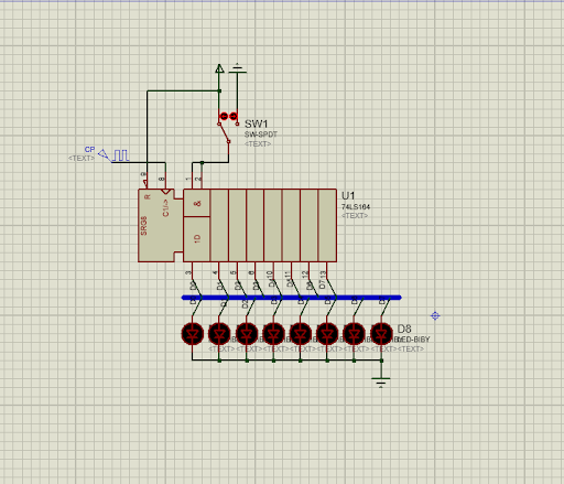
Figure 6: Proteus Simulation of 74LA123
The connections must be created cleanly and clearly to ensure the right output.
Click on the play button presented on the left side of the screen to start the simulation.
74LS164 Working of Project
Once the project is complete, you will see the following points:
The circuit does not show any output on the LEDs when the circuit is played. At this point, the LM317 does not get any input.
Once the negative input is provided to the switch, the LEDs start showing the output one after the other. This shows the logic HIGH on the bits after the regular interval.
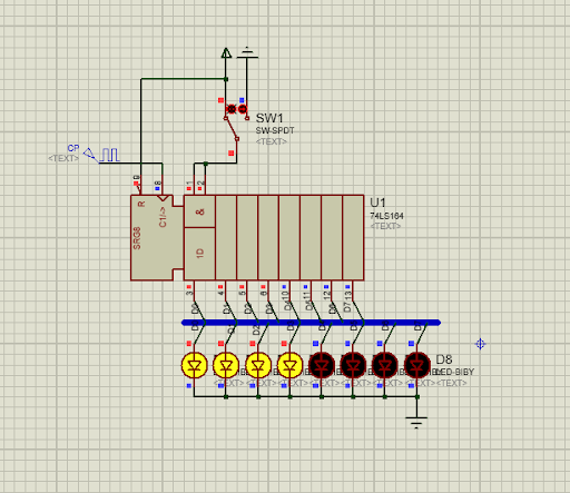
Figure 7: output of 64LS164 circuit with a switch on the negative side
Now, use the switch to provide the positive bit to the circuit, and the output on the LEDs will be shifted to the right.
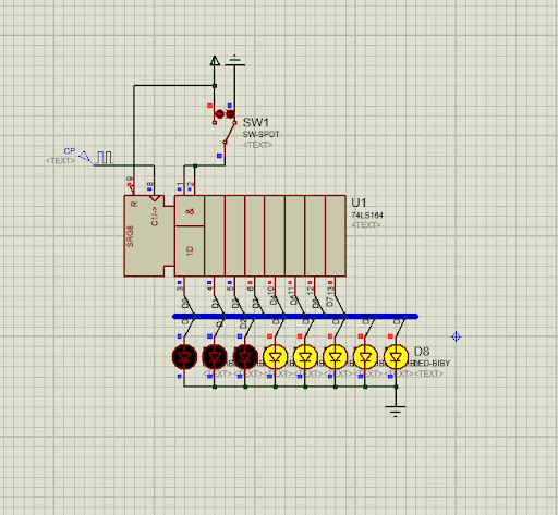
Figure 8: 74LS164 output when the plus side of the switch is on
As a result, the LEDs will show the LOW output one after the other and in the end, it will show the LOW output at every LED.
If you want to test the circuit by yourself, download the simulation from the link given here:
74LS164 working Porteus Simulation
74LS164 Features and Specifications
The basic features and specifications of the 74LS164 are given next:
Characteristic |
Value |
Description |
Operating Voltage |
3V - 18V |
Range of input voltage for proper operation |
Maximum Supply Voltage |
5.25 V |
The absolute maximum voltage that can be applied to the device |
Propagation Delay Time |
25 ns |
Time for a signal to travel through the device's internal circuitry |
Maximum Clock Frequency |
36 MHz |
The highest clock rate at which the device can reliably function |
Operating Temperature Range |
0°C to +70°C |
Environmental temperature range for reliable operation |
Clock Buffering |
Fully Buffered |
Internal clock buffering for improved signal integrity and noise immunity |
Available Packages |
16-pin PDIP, GDIP, and PDSO |
Different physical package options for PCB mounting |
Logic Family |
74LS (Low-power Schottky) |
A specific logic family with tradeoffs in speed and power consumption |
Power Consumption |
(Typical) 75 mW |
Average power is drawn during operation |
Output Current |
15 mA |
The maximum current that can be sourced or sunk by the outputs |
Fan-out |
10 LS-TTL Loads |
The number of logic gates that can be driven by a single output |
Input Threshold Voltage |
1.3 V |
Minimum input voltage level to reliably recognize a logic high |
Table 3: Features and Specifications of 74LS164
74LS164 Physical Dimensions
Just like other integrated circuits, the physical dimensions of the 74LS164 are also described in two units:
The metric dimensions are those in which the units used are the following:
Millimetres (mm)
Centimeters (cm)
Meters
Kilograms
Seconds
On the other hand, imperial units are those where the used units are the following:
Inches
Feet
Pounds
The dimensions of 74LS164 are given in the table:
Dimension |
Metric (mm) |
Imperial (inches) |
Length |
19.30 ± 0.30 |
0.760 ± 0.012 |
Width |
6.35 ± 0.25 |
0.250 ± 0.010 |
Height |
3.94 ± 0.25 |
0.155 ± 0.010 |
Pin spacing |
2.54 ± 0.10 |
0.100 ± 0.004 |
Table 4: Physical dimensions of the 74LS164
74LS164 Application
As mentioned before, the 74LS164 is a versatile register IC. It has multiple applications mentioned here:
74LS164 in Arithmetic Logic Register
The feature of the 74LS164 to store memory temporarily is useful in applications like the arithmetic logic register. Moreover, on the same device, it also shifts the data within the arithmetic logic register. Here, the main purpose of using 74LS164 is to use serial or parallel data handling.
74LS164 in Sequence Generator
The sequence generator requires the shifting and storing of the bit values. This can easily be done with the 74LS164 IC.
74LS164 in Digital Up and Down Counter
74LS164 is part of a large digital circuit. In digital up and down counters, this IC has applications because it has a sequential counting feature and when clock pulses are applied, it can decrement the values accordingly.
74LS164 in Converter
The basic feature of this IC is the serial to parallel output conversion. This feature makes it ideal for the circuit such as parallel to the serial output and vice versa.
So, in this article, we study the 74LS164 register IC in detail. We started with the basic introduction and then saw the details of the datasheet. There, we saw circuit diagrams, truth tables, logical circuits, and other related features to understand the basics of this IC. After that, we learned the working principle so that we could use it in the proteus simulation. Once we saw the results of the simulation, we studied the features and specifications of this IC, and in the end, we saw the applications of 74LS164. I hope we covered all the points but if something is missing, you can suggest it in the comment section.


