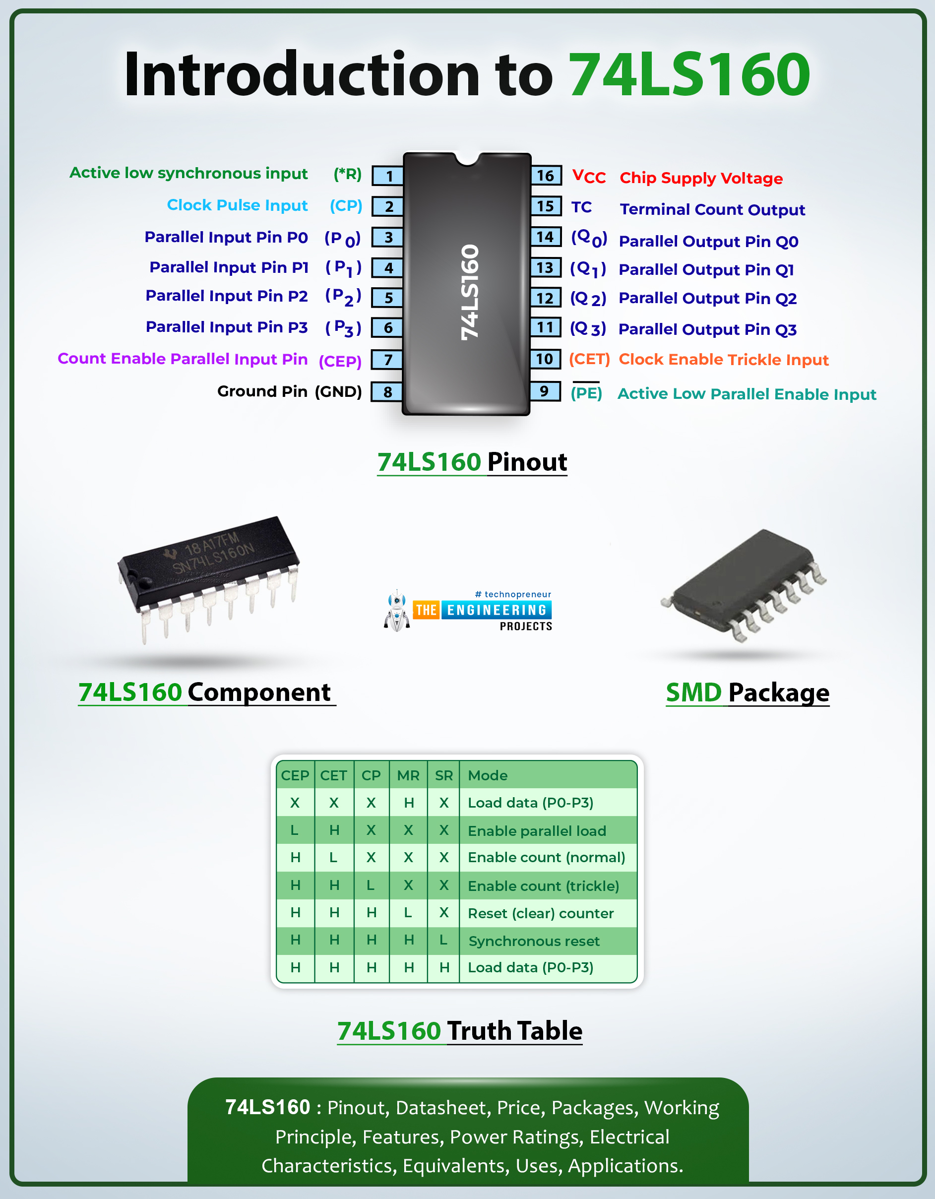
Hello students! Welcome to another tutorial on the integrated circuit in Proteus. Different integrated circuits are revolutionizing the electronic world and today we are discussing one of them. The core topic of this tutorial is the 74LS160 IC in the proteus but before that, we’ll understand the basics of this IC.
In this article, we’ll start learning the 74LS160 from scratch. We’ll see its introduction and datasheet in detail. You will see the truth table, logic diagram, and pinouts of this IC in detail, and then we’ll move on to the basic features of this IC. You will see the simulation of 74LS160 in Proteus and in the end, we’ll go through some important applications of this IC. Let’s move towards the introduction first.
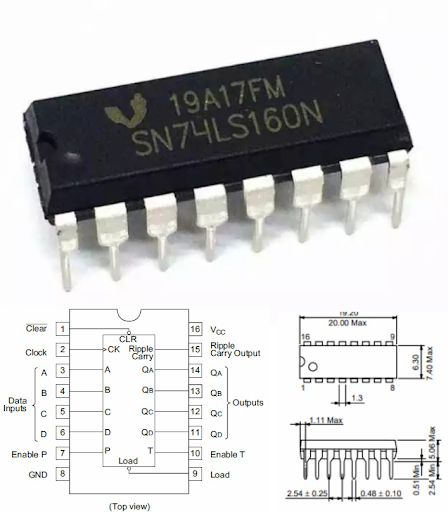
Figure 1: Top view of 74LS160 IC
74LS160 Introduction
74LS160 is an integrated circuit (IC) that is used as a counter in digital electronics.
It is a 4-bit binary synchronous counting device.
It belongs to the family of the 74xx series of ICs and the letters LS indicate that these belong to the low-power Schottky series.
This IC is made with the transistor transistor logic (TTL) technology.
It is an edge-triggered and cascadable MSI building block for multiple purposes, such as counting, memory addressing, frequency division, etc.
Moreover, it is widely used in digital circuits because it is presettable; that is, it can be used as the initial counter.
A feature of this series is that it has an asynchronous Master Reset (Clear) input that acts as an independent input, and the cock or other inputs do not control it.
74LS160 Datasheet
Before using any digital IC, it is important to understand its structure and datasheet. The details given below will help you understand the workings of this IC:

74LS160 Pinout Configuration
The 74LS160 is 16 in IC and here is its connection diagram, DIP:
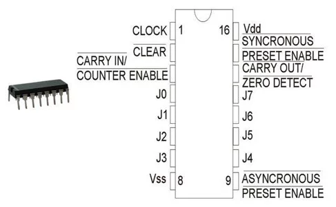
Figure 2: Pinout configuration of 74LS160
You can see that each pin has a name and number associated with it. The details of each pin can be seen in the table given next:
Symbol |
Name |
Description |
PE |
Parallel Enable (Active LOW) Input |
Enables parallel loading of data into the counter |
P0–P3 |
Parallel Inputs |
Four parallel data inputs for loading the counter |
CEP |
Count Enable Parallel Input |
Enables counting when asserted (Active LOW) |
CET |
Count Enable Trickle Input |
Enables counting when asserted (Active LOW) |
CP |
Clock (Active HIGH Going Edge) Input |
Clock input for synchronous counting (Active on rising edge) |
MR |
Master Reset (Active LOW) Input |
Resets the counter to 0 when asserted (Active LOW) |
SR |
Synchronous Reset (Active LOW) Input |
Resets the counter synchronously (Active LOW) |
Q0–Q3 |
Parallel Outputs (Note b) |
Four parallel binary outputs represent the count |
TC |
Terminal Count Output (Note b) |
Indicates when the counter reaches its maximum count |
Table 1: Pinout configuration of 74LS160
74LS160 Logic Symbol
In different cases, when the 74LS160 is shown with the logic symbol given here:
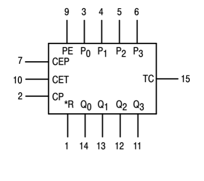
Figure 3: Logic Symbol of 74LS160
Here, pin 16 is used for the power input and pin 8 is used as the ground. The names and numbers of the pins are the same as given before in the form of the table.
74LS160 Truth Table
The truth table of this IC will help you understand the output of 74LS160 when the specific combination of inputs is fed into it. But before this, it is important to understand the following denotations in the table:
X = Don't-care condition
L = Logic low or ground
H = Logic high or positive voltage
CEP = Count Enable Parallel Input
CET = Count Enable Trickle Input
CP = Clock (Active HIGH Going Edge) Input
MR = Master Reset (Active LOW) Input
SR = Synchronous Reset (Active LOW) Input
CEP |
CET |
CP |
MR |
SR |
Mode |
X |
X |
X |
H |
X |
Load data (P0-P3) |
L |
H |
X |
X |
X |
Enable parallel load |
H |
L |
X |
X |
X |
Enable count (normal) |
H |
H |
L |
X |
X |
Enable count (trickle) |
H |
H |
H |
L |
X |
Reset (clear) counter |
H |
H |
H |
H |
L |
Synchronous reset |
H |
H |
H |
H |
H |
Load data (P0-P3) |
Table 2: Truth table of 74LS160
74LS160 Working Principle
The working principle of 74LS160 can be understood with the help of some important points about its internal structure. The basis of its working principle is to understand that when the clock pulse is applied to the 74LS160, it responds to it and counts the binary values. Here are the important points to understand this:
74LS160 Counter Bits
Since the beginning, we have been mentioning that it is a 4-bit counter. It means it can count from 0000 to 1111 in binary numbers.
74LS160 Clock Input
As with other integrated circuits, the counter responds to the clock pulse applied to its clock input. The rise in the clock input stimulates the counter operations.
74LS160 Parallel Load Inputs
The parallel load inputs are denoted by P0 to P3. The counter allows the parallel loading of the data when the appropriate pattern of signals is applied at the input pins.
74LS160 Cascading
Cascading is the process in which two or more integrated circuits are connected with each other in such a way that the output of one circuit becomes the input of the other. This is done to enhance the working ability of the system or is crucial when higher calculations are required using the counter.
The 74LS160 allows the cascading process. In this case, the ripple carry output (RCO) is connected with the clock input of the next counter.
74LS160 Simulation in Proteus
Now, it is better to understand how to create the circuit of this IC in the Porteus simulator before using it in the circuit. Here is the way to create the circuit:
Material Required
74LS160
Switch
LED
Clock
Ground
Power
Procedure
Fire up the proteus software.
Choose the first three components from the list given above.
Place them in the working area to create the circuit.
Now, go to terminal mode from the left side of the screen and choose ground terminal. Place it in the respected area.
Repeat the above step for the power terminal.
Now go to generation mode and choose the Dclock.
Place the clock on pin 2 of IC.
Connect the component through the connecting wires.
The circuit must look like the image given here:
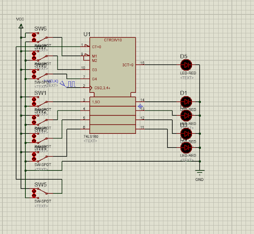
Figure 4: Proteus Circuit for 74LS160
The circuit is now ready to work. Click on the play button to start the working of the circuit.
74LS160 Circuit Working
The switches are used to provide the input signal to the circuit. When the switch is on, the input signal to the respective pin is HIGH, otherwise low.
At the start, the LEDs are working in a particular manner that the output is on all the pins in a particular pattern.
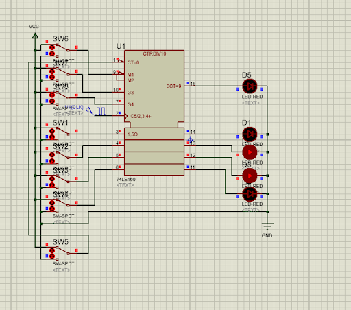
Figure 4: Changing the input of the 74LS160 circuit
Change the input through the switches and you will observe the change in the output.
You will observe a change in the values of output when the signal on the input signals is changed.
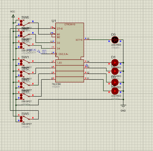
Figure 5: Getting the output of the 74LS160 Circuit simulation
The inputs and outputs are the same as given in the truth table.
If you want to have the design of the Proteus project I am using, then you can download it through the link given next:
Proteus simulation for the basic working of 74LS160
74LS160 Features and Specifications
The 74LS160 has different modes and studying all of these will help you to understand the features and specifications.
74LS160 Counting Mode
On reaching the clock edge, a pulse propagates that stimulates the counter to work.
The master-slave FF is the pulse that triggers the master-slave flip-flop structure of this IC. The state of the internal logic circuit is changed according to the structure of the IC. The details of these inputs are given in the table given before.
The logic gates of flip-flops determine the output of the IC. Usually, the output depends on the following factors:
The current state of the pins
Previous inputs of pins
Feedback connections.
In some versions, 75LS160 has the decade working, which means these can provide values between 0 and 9.
The state of the master flip flop is transferred to the corresponding slave flip flop after some time. This is done to provide a stable and more synchronized output.
74LS160 Preset Mode
During the processing, the low signals on the load input activate the logic path of the IC.
All the values in the data inputs are transferred directly to the respective flip-flops.
The process of overriding the current counter bypasses the internal counter logic. It also sets the counter’s desired initial values and this is done by presetting the counter.
74LS160 Reset Mode
The reset pin is the active low pin, which means the output is reset when this pin has a zero value.
The clearing of the flip flop is the situation when all the FFs are forced to reset their values, no matter what the values on their inputs or what the values of the clock are.
74LS160 Carry Out (CO)
The logic gates in the structure of the integrated circuit determine the internal structure of the flip flops. These are particularly useful for the transition from 1001 to 0000, which is 9 to 0 in the decimal numbers.
When the transition of the carry-out goes high, it indicates that the count cycle is complete.
The carryout pulse can be used in the cascading counter to enhance the working ability of the circuit using 74LS160.
74LS160 Physical Dimensions
If you want to use the 74LS160 in your circuits, you must know the physical dimensions of this IC. There are two basic units to measure the physical dimensions of devices like ICs:
Metric Package
In the metric package, only metric units are used to represent the calculations. The following are some of the basic units in this system:
Millimetres (mm)
Centimeters (cm)
Meters
Kilograms
Seconds
Usually, in the representation of the physical dimensions of the ICs, like 74LS160, millimeters are used for metric packages.
Imperial Package
The imperial units are also known as the British imperial units. The popular units in the imperial packages are:
Inches
Feet
Pounds
The physical dimensions of the ICs in the imperial package are mostly inches. Here is the table that clearly shows the physical calculations of the 74LS160 IC:
Dimension |
Metric (mm) |
Imperial (inches) |
Length |
19.30 ± 0.30 |
0.760 ± 0.012 |
Width |
6.35 ± 0.25 |
0.250 ± 0.010 |
Height |
3.94 ± 0.25 |
0.155 ± 0.010 |
Pin spacing |
2.54 ± 0.10 |
0.100 ± 0.004 |
Table 3: Physical dimensions of 74LS160
74LS160 Applications
The following are some prime applications where the 74LS160 is extensively used:
74LS160 as Digital Counter
The most common example of the application of this IC is to use it as a digital counter. When the clock pulse is applied to this IC, it represents the binary counting values. This is not only used as it is but usually other logic gates are combined with it to get the complex calculator to work.
74LS160 Frequency Divider
The frequency divider is the circuit that is designed to determine the value of frequency after dividing it by the power of 2. This circuit is incomplete without the 74LS160 IC.
74LS160 Timer Circuits
This IC is incorporated into the time circuits, where its main job is to generate a time delay. Moreover, it also triggers specific events based on certain conditions. These conditions are set during the design process of the circuit.
74LS160 in Sequential Logics
In the sequential logic, the 74LS160 is used as the counter. The output of this IC is used as the input of some other devices and this creates the basis of the sequential logic circuits.
74LS160 in Signal Processing Circuits
Signal processing is an important field where complex circuits are used. This IC is used in devices for signal processing where counting and timing functions are required.
Hence, today, we have seen the details of the 74LS160 Integrated Circuit. We started with the basic introduction of this IC and understood the structure and output of every pin through its datasheet. Through the logic diagram, logic circuit, truth table, and the pinouts of this IC we understood the details of its functionalities. Moreover, we saw its basic features and mode of operation. The physical dimensions of this IC made clear the domains of its usage in different circuits. We saw the simulation of the 74LS160 in the proteus and in the end, we shed light on different applications where the 74LS160 plays a vital role. I hope you have understood all the information but if you feel something missing or have any questions, you can ask us.


