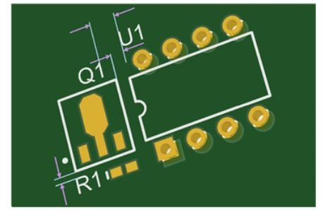
Hi, I hope you all are doing great. Today we are talking about the silkscreen on the printed circuit boards (PCBs). We know that PCBs are the essential parts of electronic devices, and there are a variety of PCBs for different circuits. Generally, silkscreening is the process of surface printing with the help of a design cut out on a sheet. But, we are particularly talking about the silkscreen on the PCB.
It is a crucial step in the PCB design and plays a role during the PCB assembly to make sure the PCB is designed well. Generally, silkscreen is used to provide basic information about the components on the PCBs. This article has a silkscreen introduction, types, and methods.
Introduction to PCB Silkscreen
The PCB Silkscreen is a layer of non-electric permanent epoxy ink present in the form of text or different graphics on the surface of PCBs. The basic use of silkscreen is to provide information, which may be the names, types, and polarity of the components. Moreover, it also includes information about the manufacturing company, such as its name or logo.
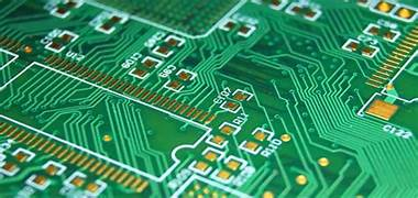
Silkscreen is also known as labelling or serigraphy and is the main technique in different industries. It is highly useful during the process of fabrication to verify the component's placement. Therefore, the PCB silkscreen helps the assembler, identify the perfect place for the components.
Multiple PCB companies offer services for prototype and assembly, and one of the most suitable names among them is PCBWay. It is a China-based company that is known for its quick services with no quality compromise. They provide the most reliable boards, and their critical testing system is responsible for the best results and top-quality PCBs.
Another advantage of choosing PCBWay Fabrication House is the competitive prices because they directly take orders and there is no need for any broker to buy the PCBs. The quick turnaround time, wide range of products, high-quality latest machines, and online status of the orders are the most significant features of PCBWay.
Silkscreen Marking Essentials
The PCB silkscreen varies depending on the design and type of the PCB, but there are some basic components of silkscreen that must be included in all silkscreens. Here are some of these:
- Names of the components along with their values
- A reference designer
- Polarity marking
- Pin-1 indicator
- Revision number
- Logo or name of the company
- Manufacturer’s identification
- Warning instructions
- Connector pinouts
Features of PCB Silkscreen
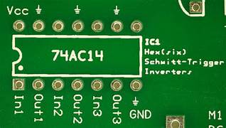
The silkscreen is a crucial tool for the perfect assembly of the PCBs. It makes sure that all the components are placed accurately and that the PCB is functioning well. There are multiple reasons to use the silkscreen, and the most important among these are given next:
Facilitation in Component Orientation
The component side of the PCB is the one where all the components of the PCB are to be mounted. The silkscreen is important to indicate the right place of the components, such as the resistors, inductors, capacitors, etc. The user simply has to follow the design on the silkscreen, and the PCB is ready to use.
Polarity and Pin Information
Many components of the circuit are polarized, such as the diode, capacitors (polarized), integrated circuits, etc. For such places in the PCB, the silkscreen has different indications, such as dots or other symbols, to identify the right direction. This facilitates the user a lot, and it is also vital for the PCB's health when the electricity passes through the circuit because the component set at the wrong polarity may damage the PCB.
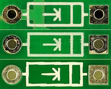
Basic Information About PCB
Silkscreen also provides information about the manufacturers, so the users do not have any difficulty dealing with the PCBs. This is because every manufacturer has a specific set of working rules. This information may include the following points:
- PCB version
- Information about the manufacturing company
- History of PCB
- Manufacturing date
This helps the users at different levels, whether they are manufacturing, placing, or using the PCB.
Aesthetic Consideration of PCB
The silkscreen makes the PCB more attractive. These are printed in a contrasting colour to the PCB surface. In this way, the PCB looks more neat and pleasing. The better the quality of the silkscreen, the better it looks. For this, more appealing colours of the silkscreen are used to enhance the texture and design.
One must know that the PCBWay offers multiple colours of ink for customers, including yellow, green, white, and black. In this way, the customers can choose the specification of PCB silkscreen of their own choice. PCBWay also provides a variety of fonts and designs; therefore, all the controls in the customer’s hand and the proper guidance of PCBWay at each step help to make your creativity live.
Methods of PCB Silkscreen Production
There are several ways of producing silkscreen and the manufacturers select the most accurate by keeping some parameters in mind. Some of such parameters are the material of the PCB, cost, creation, and manufacturer of the silkscreen. Some of the most important methods that you must know are given here:
Liquid Photo Imaging (LPI)
This technique is known for its high-resolution results, and it does not require a printing plate because it uses liquid plates. An advantage of using it is its ability to avoid shorts and maintain the PCB’s electrical integrity. This method uses liquid curable inks that are cured with UV lights. A design is applied to the lights so that only the required area is hardened, and then the unwanted part is removed. This design is now used for the silkscreening process on PCBs.
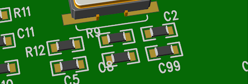
When the laser is applied to the protective layer of the PCB, the copper underneath is exposed and as a result, the PCB is ready for more processes.
Manual Screen Printing
This is the most traditional method for PCB silkscreen and is also known as Hand screen printing for PCB. In this process, the stencil is created on the mesh. The ink is applied to the mesh, and a squeegee is used to force the ink onto the surface of the PCB. The mesh or stencil has a specific design according to the requirements, and as a result, the silkscreen is printed on the surface.
Direct Legend Printing
The principle of this type of printing is the same as that of the inkjet printer. The high-speed inkjet printer is used to print the board directly. The acrylic ink is applied directly to the CAD data. This ink is then cured with UV lights during the printing process. Usually, DLP is applied to the PCB after the application of the solder mask. This is a quick method that involves fewer steps, but the users get high efficiency and precision. Moreover, factors such as setting the font size and style are under the control of the designers.

Name of Technique |
Advantages |
Disadvantages |
Liquid Photo Imaging |
Precision, Requires less area |
More time and ink are required to set |
Manual Screen Printing |
Cost-effective, Easy to use |
Require larger area, Not suitable for large-volume |
Direct Legend Printing |
Low dry time, Highest accuracy |
Can not apply to silver-based PCBs |
If we talk about the prominent name dealing with the silkscreen then the PCBWay is one of the best options. It provides all these methods to their buyers and also guides them about the best choice of silkscreen they must have. Moreover, they provide versatility in the design options to make your PCB exceptional. I hope you have gotten all the information you were searching for. The silkscreen is a crucial process during the manufacturing of PCBs. It provides facilitation for the user and manufacturer. There are multiple ways of PCB silkscreen manufacturing, and the user has to choose the best according to the circuit. If you need some help with the topic, you can contact us.


