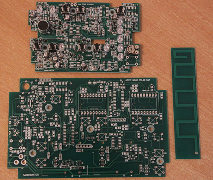
Printed circuit board is a very important part of electronic devices. You will find them in all electronic appliances. To make a good quality PCB, it is very important to select high-grade materials. A PCB mainly consists of a NON-conductive material. Conductive lines are etched or printed on them.
PCB materials are mainly of 3 types.
- FR-4
- Teflon
- Metal
Among these 3, FR-4 is the most common. This article will discuss all that you need to know about FR4 PCB Fabrication. We will discuss all about FR4. We will focus on its advantages.
FR-4 Manufacturing
- PCBway Fabricaton House manufactures high-quality FR4 PCBs. They can produce these PCBs really fast. The cost is also optimum. They are capable of making multi-layered FR4 PCBs.
Here are some samples of FR4 PCBs made by PCBway.

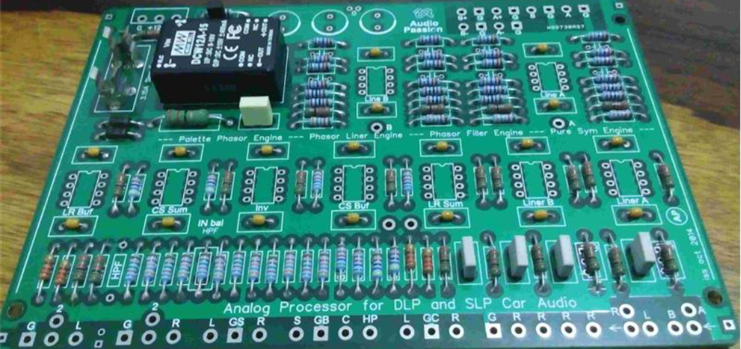
Here are some common FR4 PCB assembly mounting technology types:
1. Surface Mount Technology (SMT):
SMT is the most widely used technology for mounting components on FR4 PCBs. In SMT, components are mounted directly onto the surface of the PCB using solder paste. The solder paste is applied to the solder pads on the PCB. Then the components are then placed on top of the solder paste. The PCB is then heated. It melts the solder. Thus it creates a permanent electrical and mechanical connection between the component leads and the PCB.
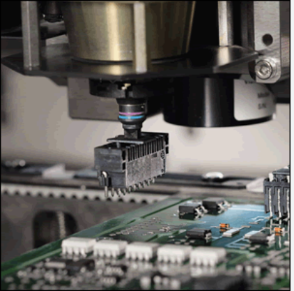
2. Through-Hole Technology (THT):
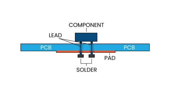
THT involves inserting component leads through holes drilled in the FR4 PCB. The leads are then soldered on the opposite side of the PCB to create a connection. THT is commonly used for components that need additional mechanical strength. THT is also used for high power or high voltage requirements.It is less commonly used than SMT. Still it is relevant for certain applications.
3. Mixed Technology:
Many PCB assemblies combine both SMT and THT components. This is called mixed technology assembly. In such cases, the SMT components are typically mounted first. After that, the THT components are inserted and soldered on the opposite side of the PCB.

4. Chip-On-Board (COB):
COB technology involves mounting bare semiconductor chips directly onto the FR4 PCB. This technology works without traditional packaged components. The chips are typically attached using conductive adhesives or wire bonding techniques. COB technology is commonly used for high-density applications where size and weight reduction are critical, such as in mobile devices.
5. Ball Grid Array (BGA):
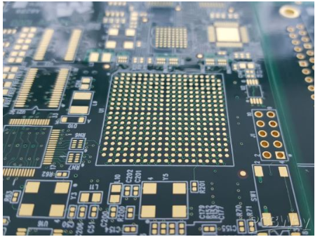
BGA is a surface mount technology that utilizes an array of solder balls on the underside of the component. These solder balls create electrical connections between the component and the PCB. BGA components offer high pin counts and are commonly used in applications that require high-performance processors, graphics chips, or other integrated circuits.
6. Micro BGA (uBGA):
Micro BGA is a variation of BGA technology that utilizes smaller solder balls and tighter ball pitches. This technology is often used for miniaturized electronic devices where space is limited.
These are some of the common FR4 PCB assembly mounting technology types. The selection of the appropriate technology depends on the specific requirements of the PCB design, the complexity of the circuit, the size of the components, and the intended application. Manufacturers consider these factors to ensure a reliable and efficient assembly process.
FR4 PCB fabrication typically involves the following steps:
1. Design:
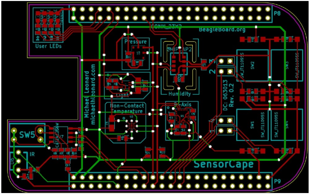
First, we need to create the PCB layout. We have to use design software like Proteus, Kicad, Eagle etc. Then we need to place components. Then we need to route the traces. At the time of routing, we should avoid DRC errors. It is very important to define the board dimensions.
Following is a typical PCB layout:
2. Gerber File Generation:
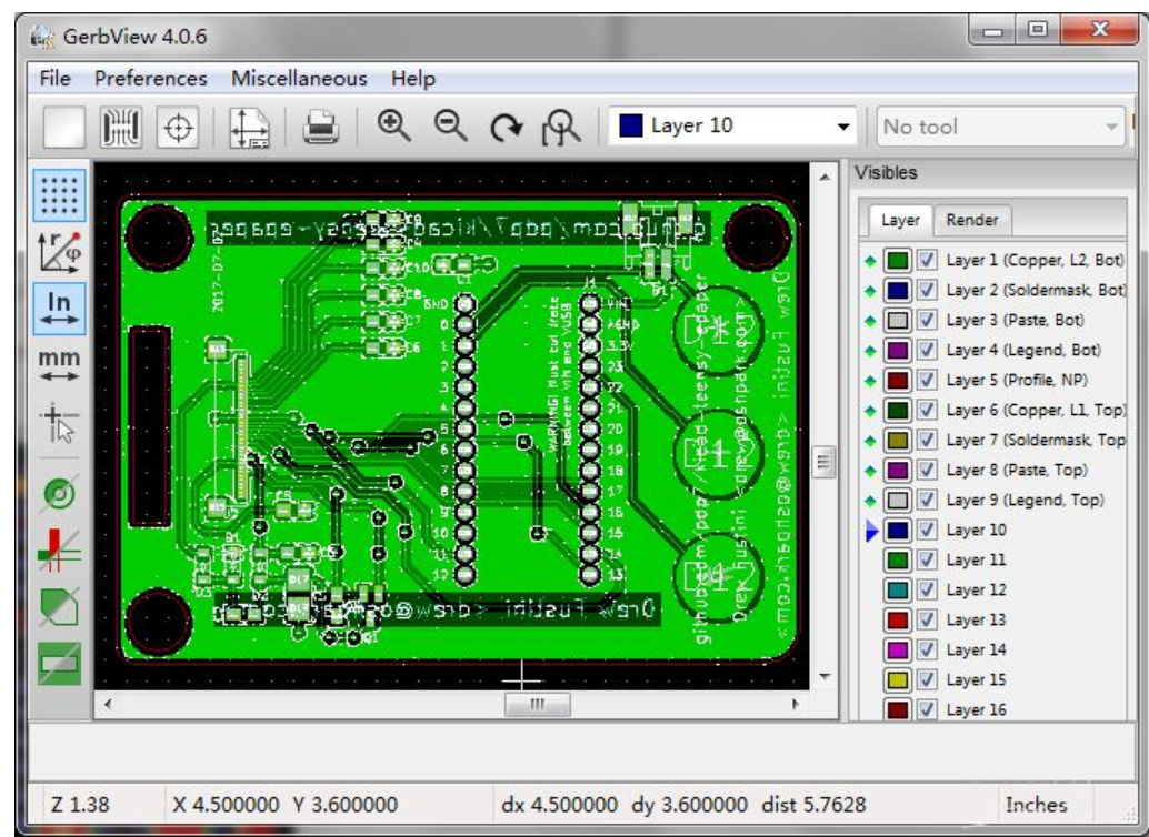
The next step is Gerber File Generation. We can Gerber files from the PCB design software. These files have the necessary information about the PCB layers, copper traces, solder masks, and other design elements.
You can generate Gerber files using Atrium, Kicad etc.
A typical gerber will look like the following picture:
3. Material Selection:
Choose the appropriate FR4 material for the PCB based on the desired electrical and mechanical properties.
Choosing the appropriate FR4 material for a PCB involves considering the desired electrical and mechanical properties. Here are some key factors to consider:
- Dielectric Constant (Dk): The dielectric constant of the FR4 material affects the impedance and signal propagation characteristics of the PCB. Higher Dk values result in slower signal speeds. Consider the specific requirements of your circuit design. Select an FR4 material with an appropriate Dk value.
- Glass Transition Temperature (Tg): Tg is the temperature at which the FR4 material transforms from a rigid state to a soft, rubbery state. Higher Tg values indicate better heat resistance and mechanical strength. Ensure that the chosen FR4 material has a Tg value that can withstand the expected operating temperatures of your PCB.
- Copper Foil Thickness: Copper foils are added to the FR4 material. The thickness of the copper foil affects the current-carrying capacity of the PCB. It also affects the PCB’s thermal performance. Thicker copper foils can handle higher currents. However, they may require more complex fabrication processes.
- Layer Count: Determine the number of layers required for your PCB design. FR4 materials are available in various layer configurations. Single-sided, double-sided, and multilayer are among those. Consider the complexity of your circuit design. Choose an FR4 material that supports the required number of layers.
- Surface Finish Compatibility: There are different kinds of surface finishes. For example-
HASL (Hot Air Solder Leveling):
HASL is a widely used surface finish for FR4 PCBs. In this process, the exposed copper pads on the PCB are coated with a layer of tin-lead solder. The PCB is then passed through a hot air leveling machine. The machine blows hot air to level and distributes the solder evenly across the surface. This ensures a flat, solderable surface for component attachment. HASL offers good solderability and robustness. It is relatively cost-effective. However, it may not be suitable for fine-pitch components due to the relatively thick solder layer.
ENIG (Electroless Nickel Immersion Gold): ENIG is a popular surface finish for FR4 PCBs.If it suitable for applications requiring good electrical performance and solderability. In the ENIG process, the exposed copper pads are first coated with a thin layer of electroless nickel. Nickel provides a diffusion barrier between the copper and the final layer. Next, a thin layer of immersion gold is deposited on top of the nickel layer. The gold layer protects the nickel from oxidation. It provides excellent solderability. ENIG offers a flat surface, good corrosion resistance, and is suitable for fine-pitch components.
OSP (Organic Solderability Preservative):
OSP is another surface finish option for FR4 PCBs. It is suitable for applications where cost and environmental concerns are important. OSP is a thin, organic coating. It is applied directly to the exposed copper pads. It provides a temporary solderable surface that protects the copper during storage and transportation. When soldering, the OSP layer is removed during the soldering process.
Supplier and Industry Standards: Consider the reputation and reliability of the FR4 material supplier. Additionally, check if the chosen FR4 material complies with industry standards, such as IPC-4101 or UL-94.
When choosing FR4 materials for PCB manufacturing, there are various supplier and industry standards that can help guide the selection process. Here are some key standards to consider:
Supplier Standards:
- a) UL Recognition: Underwriters Laboratories (UL) is a globally recognized safety certification organization. They provide testing and certification services for electrical components and materials, including FR4 laminates. UL recognition ensures that the FR4 material meets specific safety and performance criteria.
- b) ISO Certification: The International Organization for Standardization (ISO) sets globally recognized standards for various industries. Suppliers with ISO 9001 certification indicate that they have implemented quality management systems to ensure consistent product quality.
- c) RoHS Compliance: The Restriction of Hazardous Substances (RoHS) directive restricts the use of hazardous substances in electrical and electronic equipment. FR4 materials should comply with RoHS regulations to ensure they do not contain restricted substances such as lead, mercury, cadmium, and others.
Industry Standards:
- a) IPC Standards: The Institute for Printed Circuits (IPC) develops and publishes industry standards for PCB design, manufacturing, and assembly. IPC-4101 is a standard that defines the requirements for base materials, including FR4 laminates. It specifies material properties such as dielectric constant, thermal conductivity, and flame resistance.
- b) NEMA Standards: The National Electrical Manufacturers Association (NEMA) sets standards for electrical equipment and materials. NEMA LI 1 is a standard that defines the performance requirements for laminated thermosetting materials, including FR4.
- c) MIL-PRF-55110: This military specification outlines the requirements for rigid printed wiring boards used in military and aerospace applications. It includes specific requirements for FR4 materials. Those are mechanical properties, electrical performance, and environmental durability.
We have to Consider these supplier and industry standards when selecting FR4 materials. This makes sure that the chosen materials meet recognized quality, safety, and performance criteria. It is essential to collaborate closely with reputable suppliers and consult relevant standards to make informed decisions regarding FR4 material selection.
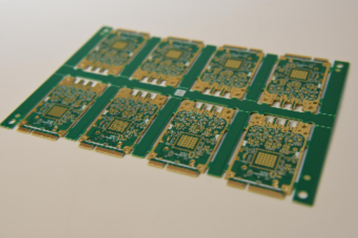
4. Panelization:
Arrange multiple PCB designs on a larger panel. It is for efficient fabrication and cost optimization. This step involves duplicating the design layout. It also adds break-off tabs for later separation.
5. Cleaning:
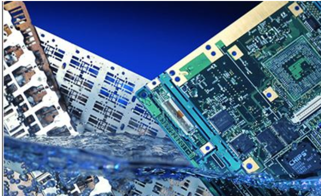
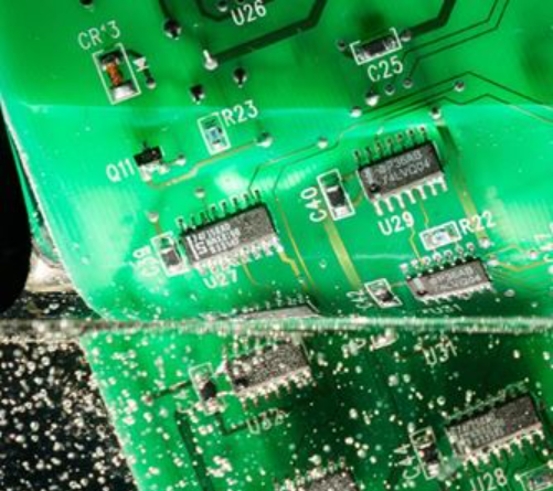
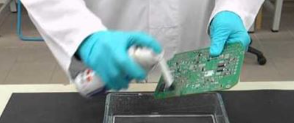
Dirt, oils, or oxidation may affect the bonding between the copper and the substrate. Clean the copper-clad FR4 material to remove these.
The following figures show different types of cleaning techniques:
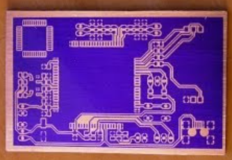
6. Imaging:
Print the Gerber files onto a photosensitive film. This process uses a machine that exposes the film to UV light through a photo tool or a film negative. The following figure shows gerber file imaging.
7. Lamination:
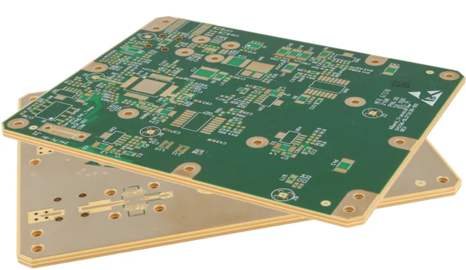
Place the photosensitive film onto the cleaned FR4 material. Pass it through a laminator. The heat and pressure bond the photoresist film to the copper layer. Following are some images of FR4 laminates.

8. Exposure:
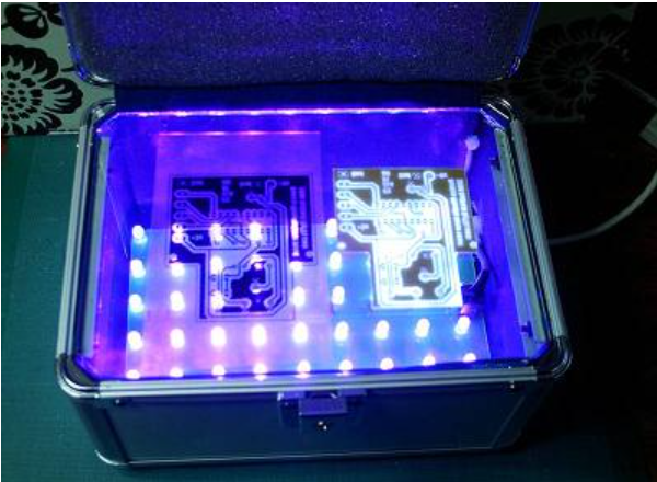
Expose the laminated material to UV light. You have to use the photo tool or film negative as a mask. The UV light cures the photoresist. UV light also hardens it in the areas not covered by the opaque parts of the mask.
9. Development:
Remove the uncured photoresist using a developing solution. This reveals the underlying copper layer. Thus it creates the required circuit pattern.
10. Etching:
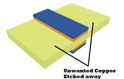
Submerge the panel in an etching solution. It’s typically a chemical mixture that removes the exposed copper. The etching process selectively removes copper. It leaves behind the circuit traces defined by the cured photoresist.
11. Stripping:
Remove the remaining photoresist from the panel.Use a stripping solution or plasma treatment. This exposes the copper traces for further processing.
12. Drilling:
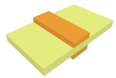
Drill holes into the panel at the designated positions. These are for component mounting and interconnection. These holes allow for the insertion of through-hole components or the formation of vias for multilayer PCBs.
13. Plating:
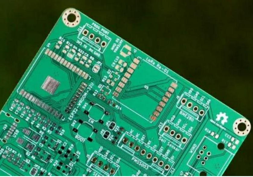
Plate the drilled holes with a conductive material, such as copper. Plating establishes electrical connections between different layers of the PCB.
14. Solder Mask Application:
Apply a solder mask layer over the surface of the PCB. Leave openings only at the solder pad locations. The solder mask protects the copper traces. It also prevents solder bridges during assembly.
15. Silkscreen Printing:
Use a silk screening process to print component identifiers, logos, and other markings onto the PCB surface. This step helps with component placement and identification.
16. Surface Finish:
Apply a surface finish to protect the exposed copper and facilitate soldering. Common surface finishes include HASL (Hot Air Solder Leveling), ENIG (Electroless Nickel Immersion Gold), OSP (Organic Solderability Preservative), and immersion tin or silver.
17. Electrical Testing:
Perform electrical tests. The tests check the functionality and integrity of the fabricated PCB. This can include tests such as continuity testing, insulation resistance testing, and high-voltage testing.
18. Routing and Separation:
Cut or route the panelized PCB into individual boards along the break-off tabs created during the panelization step.
19. Final Inspection:
Inspect the finished PCBs for any visual defects. There may be solder mask misalignment, open or shorted traces, or incorrect component markings. Correct these errors.
20. Packaging and Shipping:
Package the PCBs appropriately. Prepare them for shipping to the intended recipients or assembly facilities.
Advantages:
FR4 fabrication is cost-effective. FR4 has excellent electrical and mechanical properties. They support a wide range of operating temperatures. They are known for excellent thermal properties. FR4 PCBs have high strength-to-weight ratios.
Conclusion:
PCBway Manufacturing House is capable of printing advanced FR4 PCBs. They have Up to 64 layer processing technology. Their PCBs are ISO/TS1694:2009 certified. They also have ISO9001:2008 quality certification. They offer efficient service and fast delivery.


