Interface PCF8591 ADC/DAC Analog Digital Converter Module with Raspberry Pi 4
Welcome back to another Python tutorial for the Raspberry Pi 4! The previous tutorial showed us how to construct a Raspberry Pi-powered cell phone with a microphone and speaker for making and receiving calls and reading text messages (SMS). To make our Raspberry Pi 4 into a fully functional smartphone, we built software in Python. As we monitored text and phone calls being sent and received between the raspberry pi and our mobile phone, we experienced no technical difficulties. But in this tutorial, you'll learn how to hook up the PCF8591 ADC/DAC module to a Raspberry Pi 4.
Since most sensors only output their data in analog values, converting them to binary values that a microcontroller can understand is a crucial part of any integrated electronics project. A microcontroller's ability to process analog data necessitates using an analog-to-digital converter.
Some microcontrollers, including the Arduino, MSP430, and PIC16F877A, contain an onboard analog-to-digital converter (ADC), whereas others, like the 8051 and Raspberry Pi, do not.
Required Components
Raspberry-pi 4
PCF8591 ADC Module
100K Pot
Jumper wires
You are expected to have a Raspberry Pi 4 with the most recent version of Raspbian OS installed on it, and that you are familiar with using a terminal program like putty to connect to the Pi via the Internet and access its file system remotely. Those unfamiliar with Raspberry Pi can learn the basics by reading the articles below.
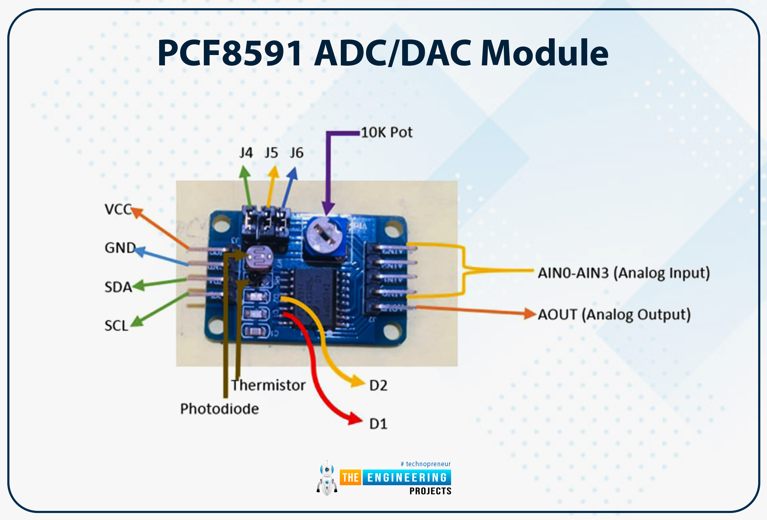
PCF8591 ADC/DAC Module
Each of the ten pins on the PCF8591 module may read analog values as high as 256 on the PCF8591's digital side or vice versa. The board has a thermistor and LDR circuit. Input and output from this module are both analogs. To facilitate the I2C protocol, it has a dedicated serial clock and serial data address pins. The supply voltage ranges from 2.5 to 6V, and the stand-by current is minimal. We can further turn the module's potentiometer knob to control the input voltage. A total of three jumpers can be found on the board. Switching between the thermistor, LDR/photoresistor, and adjustable voltage access circuits is possible by connecting J4, J5, and J6. D1 and D2 are two LEDs on the board, with D1 displaying the strength of the output voltage and D2 indicating the power of the supply voltage. When the supply or output voltage is increased, the brightness of LEDs D1 and D2 are correspondingly enhanced. Potentiometers connected to the LEDs' VCC or AOUT pins also allow testing.
Microprocessors, Arduinos, Raspberry Pis, and other digital logic circuits can interact with the physical environment thanks to Analogue-to-Digital Converters (ADCs). Many digital systems gather information about their settings by analyzing the analog signals produced by transducers such as microphones, light detectors, thermometers, and accelerometers. These signals constantly vary in value since they are derived from the physical world.
Digital circuits use binary signals, which can only be in one of two states, "1" (HIGH) or "0" (LOW), as opposed to the infinitely variable voltage values provided by analog signals (LOW). Therefore, Analogue-to-Digital Converters (A/D) is an essential electronic circuit for translating between constantly varying analog impulses and discrete digital signals.
To put it simply, an analog-to-digital converter (ADC) is a device that, given a single instantaneous reading of an analog voltage, generates a unique digital output code that stands in for that reading. The precision of an A/D converter determines how many binary digits, or bits, are utilized to represent the original analog voltage value.
Analogue and Digital Signals
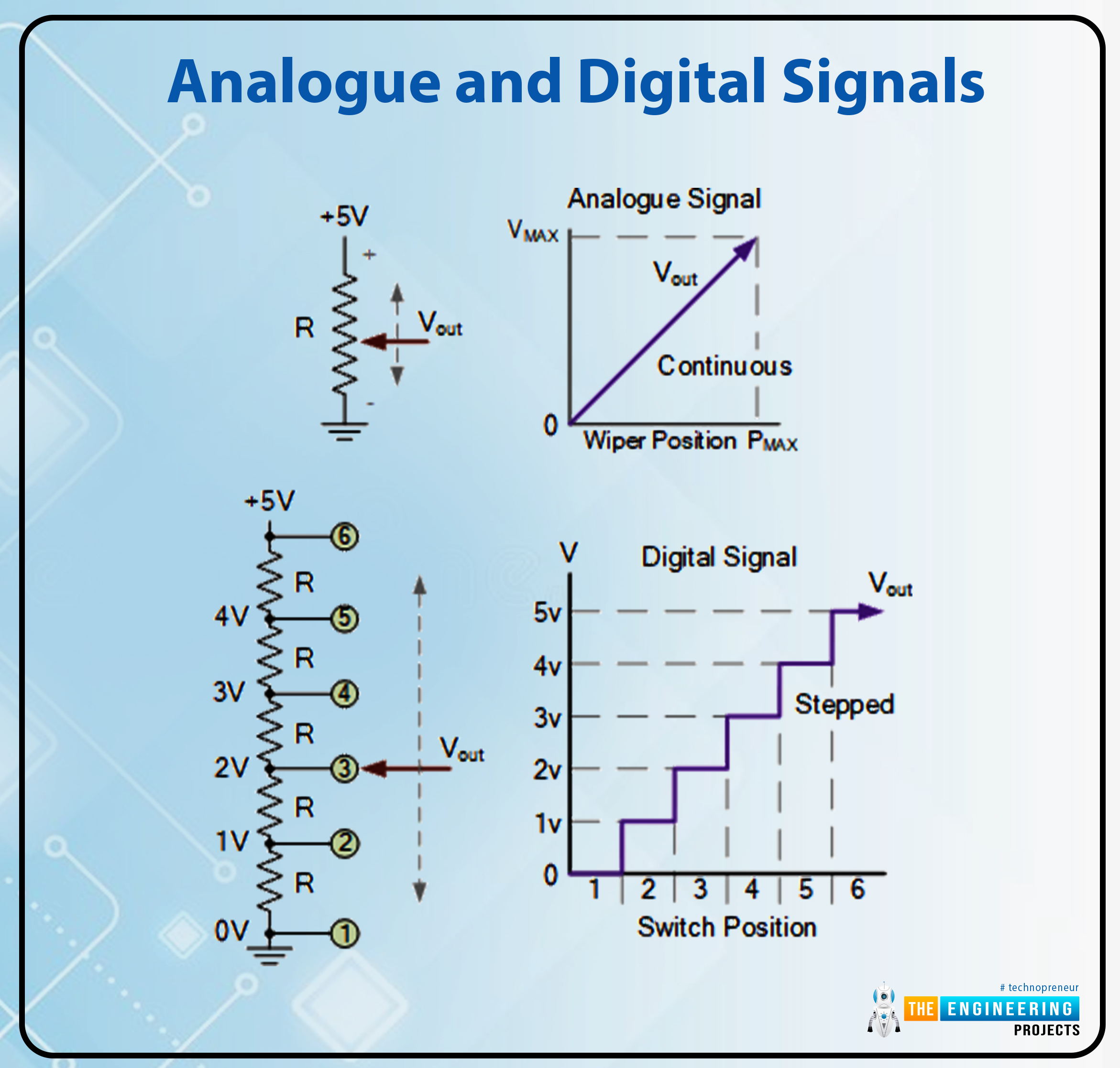
By rotating the potentiometer's wiper terminal between 0 and VMAX, we may see a continuous output signal with an endless set of output values related to the wiper position. In a potentiometer, the output voltage constantly varies while the wiper is moved between fixed positions. Variations in temperature, pressure, liquid levels, and brightness are all examples of analog signals.
A digital circuit uses a single rotary switch to control the potential divider network, taking the place of the potentiometer's wiper at each node. The output voltage, VOUT, rapidly transitions from one node to the next as the switch is turned, with each node's value representing a multiple of 1.0 volts.
The output is guaranteed at 2-volt, 3-volt, 5 volts, etc., but NOT a 2.5-volt, 3.1-volt, or 4.6-volt output. Using a multi-position switch and more resistive components in the voltage-divider network, resulting in more discrete switching steps, would allow for generating finer output voltage levels.
By this definition, we can see that a digital signal has discrete (step-by-step) values, while an analog signal's values change continuously over time. We are going from "LOW" to "HIGH" or "HIGH" to "LOW."
So the question becomes how to transform an infinitely variable signal into one with discrete values or steps that a digital circuit can work with.
Converting from Analog to Digital
Although several commercially available analog-to-digital converter (ADC) chips exist, such as the ADC08xx family, for converting analog voltage signals to their digital equivalents, a primary ADC can be constructed out of discrete components.
Using comparators to detect various voltage levels and output their switching signal state to an encoder is a straightforward method known as parallel encoding, flash encoding, simultaneous encoding, or multiple comparator converters.
The equivalence output script for a given n-bit resolution is formed by a chain network of accuracy resistors and a series of comparators that are connected but equally spaced.
As soon as an analog signal is provided to the comparator input, it is evaluated with a reference voltage, making parallel converters advantageous because of their ease of construction and lack of need for timing clocks. The following comparator circuit may be of interest.
A Logic Comparator
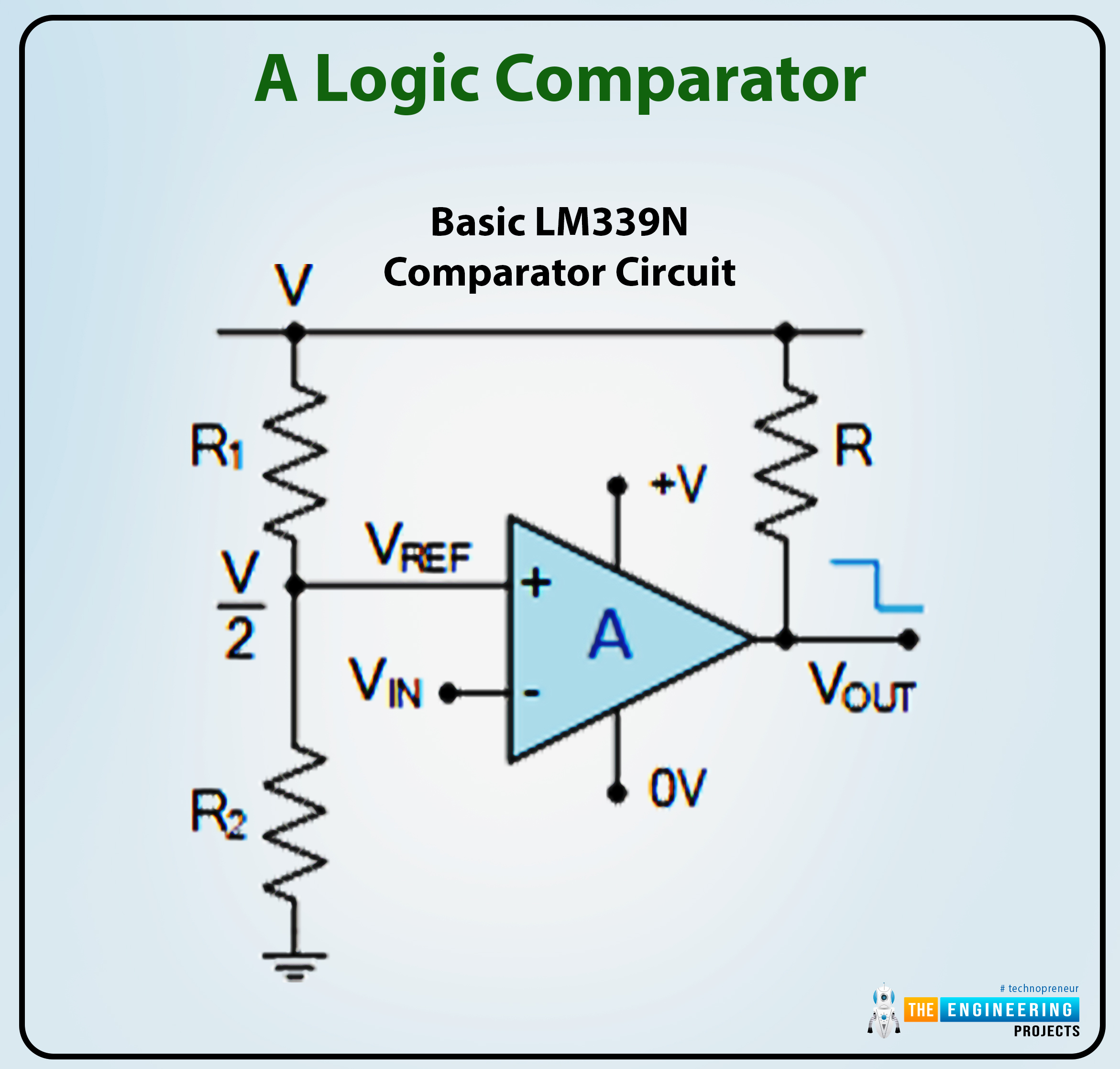
The LM339N is an analog comparator that compares the relative magnitudes of two voltage levels via its two analog inputs (one positive and one negative).
The comparator receives two signals, one representing the input voltage (VIN) and the other representing the reference value (VREF). The comparator's digital circuits state, "1" or "0," is determined by comparing two output voltages at the input of the comparator.
One input (VREF) receives a reference voltage, and the other input (VIN) receives the input voltage to be compared to it. Output is "OFF" by an LM339 comparator when the input power is lower than (VIN VREF) and "ON" when the input power is higher than the standard voltage (VIN > VREF). A comparator is a device to determine which of two voltages is greater.
Using the potential divider network established by R1 and R2, we can calculate VREF. If the two resistors are identical in value (R1 = R2), then the reference voltage will be half the input power (V/2). Therefore, like with a 1-bit ADC, the output of an open-collector comparator is HIGH if VIN is lower than V/2 and LOW otherwise.
However, by increasing the number of resistors in the voltage divider circuit, we can "divide" the voltage source by an amount equal to the ratio of the resistors' resistances. However, the number of comparators needed increases with the number of resistors in the voltage-divider network.
For an "n"-bit binary output, where "n" is commonly between 8 and 16 bits, a 2n- 1 comparator would be needed in general. As we saw previously, the comparator utilized by the one-bit ADC to determine whether or not VIN was more significant than the V/2 voltage output was 21 minus 1, which equals 1.
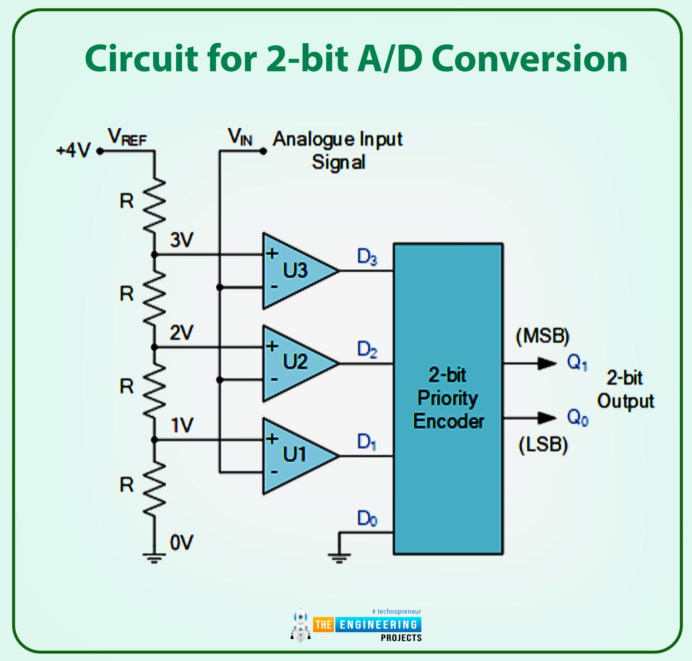
If we want to build a 2-bit ADC, we'll need 22-1 or "3" comparators since the 4-to-2-bit encoder circuitry depicted above requires four distinct voltage levels to represent the four digital values.
Circuit for 2-bit A/D Conversion
For each of the four potential values of the analog input of:
A/D Conversion Output, 2-Bit
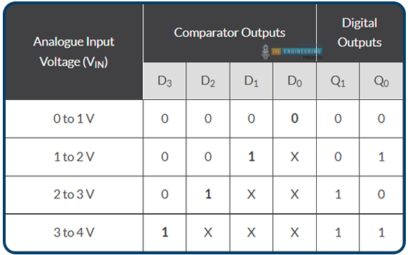
Where X is a "don't care" statement, representing a logical 0 or 1.
Explain how this analog-to-digital device operates. An analog-to-digital converter (A/D) must generate a faithful digital copy of the Analog input signal to be of any value. To keep things straightforward, we've assumed that VIN is somewhere between 0 and 4 volts and have adjusted VREF and the voltage divider network so that there is a 1 V drop between each resistor in this simple 2-bit Analog - to - digital example.
A binary zero (00) is output by the encoder on pins Q0 and Q1 when the input voltage, VIN, is less than the reference voltage level, which occurs when VIN is between 0 and 1 volts (1V). Since comparator U1's reference voltage input is set to 1 volt, when VIN rises above 1 volt but is below 2 volts, U1's HIGH output is triggered. When the input changes at D1, the priority encoder, used for the 4-to-2-bit encoding, generates a binary result of "1." (01).
Remember that the inputs of a Priority Encoder, like the TTL 74LS148, are all assigned different priority levels. The highest priority input is always used as the output of the priority encoder. So, when a higher priority input is available, lesser priority inputs are disregarded. Therefore, if there are many inputs simultaneously at logic state "1", only the input with high priority will have its output code reflected on D0 and D1.
Thus, now that VIN is greater than 2 volts—the next reference voltage level—comparator U2 will sense the difference and output HIGH. However, when VIN is more than 3 volts, the priority encoder will output a binary "3" (11), as input D2 has a high priority than inputs D0 and D1. Each comparator outputs a HIGH or LOW state to the encoder, generating 2-bit binary data between 00 and 11 as VIN decreases or changes between every reference voltage level.
This is great and all, but commercially available priority encoders, like the TTL, are 8-bit circuits, and if we use one of these, six of the binary numbers will go unused. A digital Ex-OR gate and a grid of signaling diodes can create a straightforward encoder circuit.
Diode-based 2-bit ADC
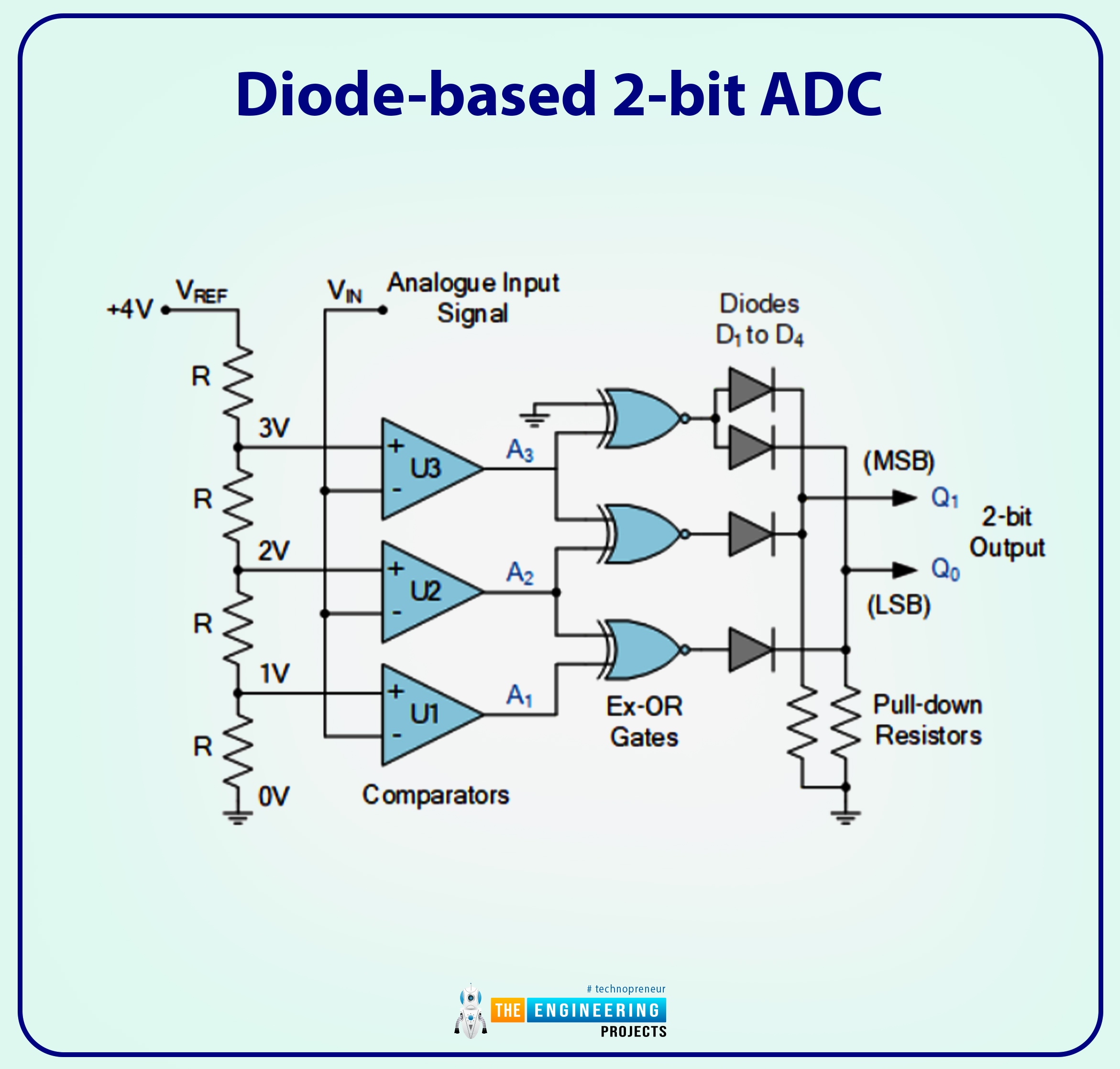
Before feeding the diodes, the results of the comparators go through an Exclusive-OR gate to be encoded. Whenever the diode is reverse biased, an external pull-down resistor is connected between the diodes' outputs and ground (0V) to maintain a LOW state and prevent the outputs from floating.
Also, as with the main board, the value of VIN controls which comparator sends a HIGH (or LOW) signal to the exclusive-OR gates, which provide a HIGH output if either of the inputs is HIGH but not both (the corresponding Boolean is Q = A.B + A.B). The AND-OR-NAND gates of combinational logic could also be used to build these Ex-OR gates.
The difficulty with both of these 4-to-2 converter designs is that the input analog voltage at VIN needs to vary by one full volt for the encoder to vary its output code, limiting the precision of the simple two-bit A/D converter to 1 volt. The output resolution can be improved by employing more comparators to convert to a three-bit A/D converter.
D/A Converter, 3-Bit
The aforementioned parallel ADC takes a voltage reading between 0 and over 3 volts as an analog input and turns it into a binary code with only 2 bits. Since there are 23 = 8 possible digital outputs from a 3-bit digital circuits system, the input analog voltage can be compared to a scale of eight voltages, each of which is one-eighth (1/8) of the voltage supply. This means that we can now measure to an accuracy of 0.5 (4/8) volts and that 23-1 comparators are needed to generate a binary code with a 3-bit resolution (from 000 (0) to 111 (7)).
Circuit for 3-bit Analog-to-Digital Conversion
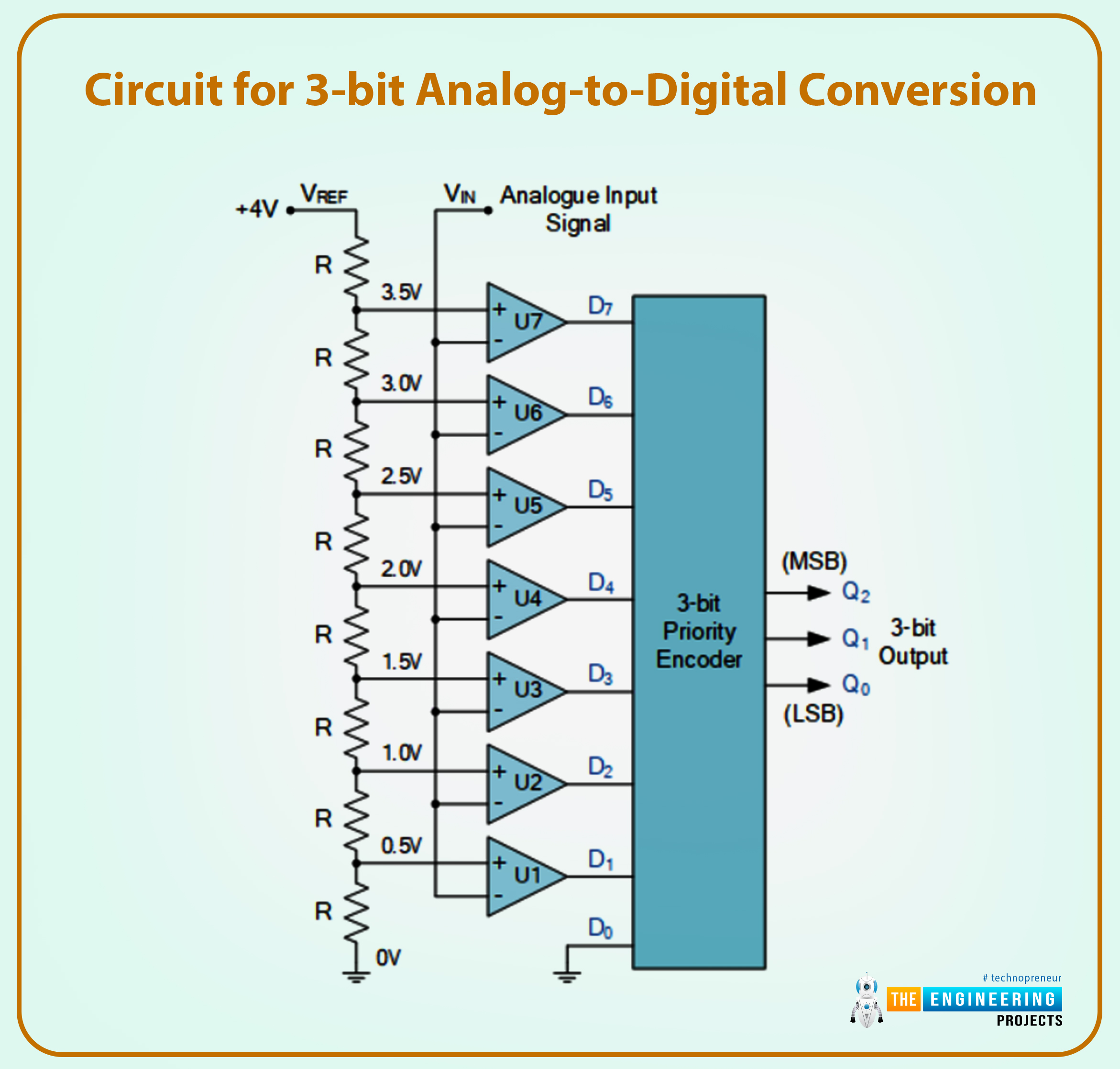
This will provide us with a three-bit code for each of the eight potential values of the analog input of:
The result of a Three-Bit Analog-to-Digital Converter
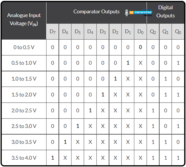
An "X" may be a logic 0 or a logic 1 to indicate a "don't care" state.
Then we can see that more comparators and power levels are required and more output binary bits when the ADC's resolution is increased.
Therefore, an analog-to-digital converter with a 4-bit resolution needs only 15 (24-1) comparators. An eight-bit resolution requires 255 (28-1) comparators. A 10-bit resolution needs 1023 comparators, etc. Therefore, the complexity of this type of Analog-to-Digital Converter circuit increases as the number of output bits increases.
Only if a few binary bits are needed to make a read on a display unit to represent the reference voltage of an input analog signal can a parallel or flashed A/D converter quickly be developed as part of a project due to its fast real-time conversion rate.
As an input interface circuit component, an analog signal from sensors or transducers is converted into a digital binary code by an analog-to-digital converter. Similarly, a digital binary code can be converted into a comparable analog quantity using a Digital-to-Analog Conversion for output interfacing to operate a motor or actuator or, more often, in audio applications.
Raspberry Pi's I2C pins
Knowing the Raspberry Pi's I2C port pins and setting up the I2C connection in the pi 4 are the initial steps in using a PCF8591 with the Pi.
GPIO2 and GPIO3 on the Rpi Model are utilized for I2C communication in this guide.
Raspberry Pi I2C Configuration
Raspberry Pi lacks I2C support by default. Therefore, it must be activated before anything else. Turn on Raspberry Pi's I2C port.
First, open a terminal and enter sudo raspi-config.
The RPi 4 Software Configuration Tool has opened.
Third, activate the I2C by selecting Interfacing options.
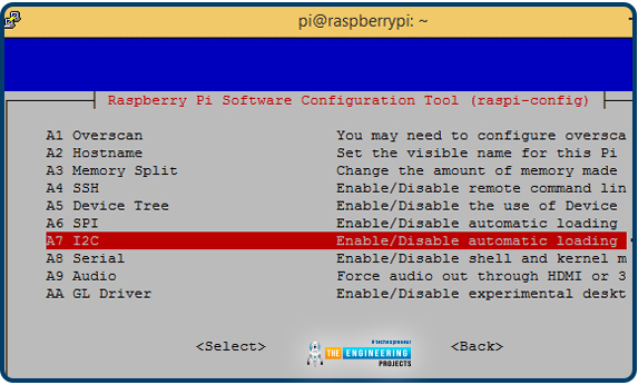
Restart the Pi after enabling I2C.
Reading the PCF8591's I2C Address with a Raspberry Pi
The Raspberry Pi has to know the I2C address of the PCF8591 IC before communication can begin. You may get the address by linking the PCF8591's SDA and SCL pins to the Raspberry Pi's own SDA and SCL jacks. The 5-volts and GND pins should be connected as well.
You may find the address of an attached I2C device by opening a terminal and entering the following command.

sudo i2cdetect –y 1 or sudo i2cdetect –y 0
After locating the I2C address, the next step is constructing the circuit and setting up the required libraries to use PCF8591 and a Raspberry Pi 4.
Connecting the PCF8591 ADC/DAC Module to the Raspberry Pi 4
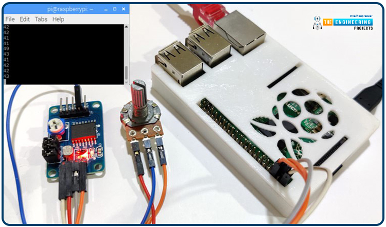
The circuit diagram to interface the PCF8591 with the Raspberry Pi is straightforward. In this example of interfacing, we'll read the analog signal from any analog inputs and display them in the Raspberry Pi terminal. We have a 100K pot to adjust the settings.
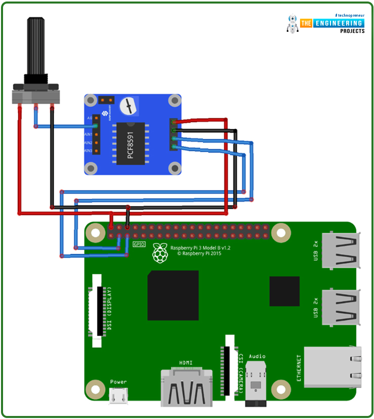
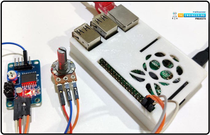
Pi's GPIO2 and GPIO must be connected to the power supply and ground. Then, hook up GPIO3 and GPIO5 to SDA and SCL, respectively. Last but not least, link AIN0 to a 100K pot. Instead of using the Terminal to view the ADC values, a 16x2 LCD can be added.
The A/D Conversion Python Program
The complete code and demo video are included after this guide.
To communicate with the I2C bus, you must first import the SMBus library and then use the time library to specify how long to wait before outputting the value.

import smbus
import time
Create some variables now. The I2C bus address is stored in the first variable, and the first analog input pin's address is stored in the second variable.

address = 0x48
A0 = 0x40
Next, we've invoked the library smbus's SMBus(1) function to create an object.

bus = smbus.SMBus(1)
The first line in the while instructs IC to take a reading from the first analog signal pin. Address information read from an Analog pin is saved as a numeric variable in the second line. Exit with the value printed.

While True:
bus.write_byte(address,A0)
value = bus.read_byte(address)
print(value)
time.sleep(0.1)
Finally, put the Python script in a file ending in.py and run it in the Raspberry Pi terminal with the command below.

python filename.py
Ensure that the I2C communication is turned on and that the pins are linked according to the diagram before running the code, or else you will get errors. It's time for the analog readings to appear in the terminal format below. The values gradually shift as you turn the pot's knob. Find out more about getting the software to work in
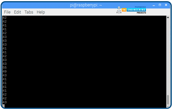
Here is the full Python script.
import smbus
import time
address = 0x48
bus = smbus.SMBus(1)
while True:
bus.write_byte(address,A0)
value = bus.read_byte(address)
print(value)
time.sleep(0.1)
ADC's Practical Uses
We rely heavily on electronic gadgets in today's high-tech society. The digital signal is the driving force behind these digital devices. While most numbers are represented digitally, few still use analog notation. Thus, an ADC is employed to transform analog impulses into digital ones. ADC can be used in an infinite variety of contexts. Here are only a few examples of their use:
The digitized voice signal is used by cell phones. The voice is first transformed to digital form using an ADC before being sent to the cell phone's transmitter.
Digital photos and movies shot with a camera can be viewed on any computer or mobile device thanks to an analog-to-digital converter.
X-rays and MRIs are just two examples of medical imaging techniques that use ADC to go from Analog to digital before further processing. Then, they're adjusted so that everyone can follow along.
ADC converters can also transfer music from a cassette tape to a digital format, such as a CD or a USB flash drive.
The Analog-to-Digital Converter (ADC) in a digital oscilloscope converts analog signals to digital ones that can then be displayed and used for other reasons.
The air conditioner's built-in temperature sensors allow for consistent comfort levels. The onboard controller reads the temperature and makes adjustments based on the data it receives from the ADC.
Nowadays, practically everything has a digital counterpart, so every gadget must also include an ADC. For the simple reason that its operations require a digital domain accessible only via an analog-to-digital converter (ADC).
Conclusion
This piece taught us how to connect a Raspberry Pi 4 to a PCF8591 Analogue - to - digital decoder module. We have observed the output being shown as integers on our Terminal. We have also researched how the ADC generates its output signals. Here we will use OpenCV and a Raspberry Pi 4 to create a social distance detector.


