How to Optimize a PCB Panel Layout
Hi Guys! Hope you’re well today. I welcome you on board. In this post, I’ll walk you through How to Optimize a PCB Panel Layout.
PCB panels are used in the manufacturing process to produce PCBs in large numbers. This not only reduces the overall cost but also makes the manufacturing process more efficient and reliable. PCB panelization is a manufacturing technique where multiple PCB designs are replicated on a single large board called a PCB panel. Then these individual boards are removed and depanelized from the panel to install them in the final product.
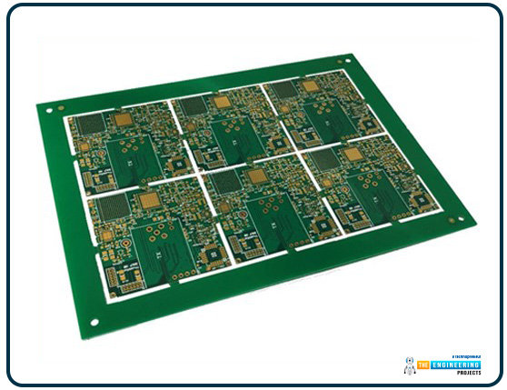
The number of panels is directly related to the overall manufacturing cost. To produce more panels, more cost will be required. However, it also depends on the shape of the board. If you require more boards of the same shape and size, it will reduce the panel cost since they all can be replicated and manufactured on a single panel.
Read on to find out how we can optimize the PCB panel layout to save both cost and time.
Let’s jump right in.
How to Optimize a PCB Panel Layout
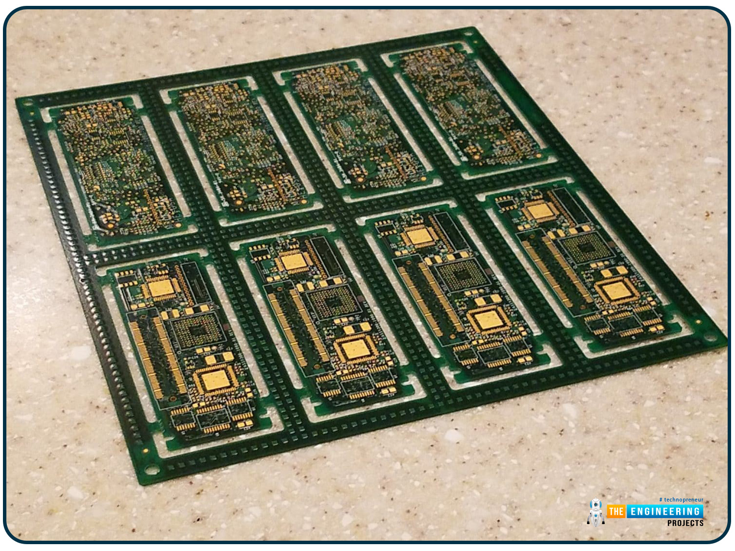
PCB panel is a large board that contains multiple instances of a small PCB. Know that the PCB panel is made up of the same material as the board and the panel size depends on the number of small boards you aim to produce. It is required to best use the panel space to produce PCBs in large numbers and to keep the unused panel space minimum. Since the more boards cover the overall panel space, the more efficient the manufacturing process will be.
PCB Panelization Layout Tips
You can pick the panel size as per your requirement. However, the most commonly used panel size is 18 x 24 inches. Normally, the boards are 0.100 inches apart in one panel. Panel designers need to be very careful while putting the PCB designs in the panel.
1: Use PCB Design Tools Efficiently
It is important to use your PCB design tools properly to avoid any hassle in the manufacturing process. Decisions made earlier during the PCB design process can go a long way and keep you from redesigning the entire board from scratch. These design tools can help you select the layer stack up configuration and PCB material. Additionally, they can help you transfer design data using open standard formats. Using this format manufacturer can exchange the design information with the PCB designers and can compile it in one file format.
2: Collaborate with PCB Designer
To make the manufacturing process efficient, it’s better that PCB designers are in contact with the PCB panel designers. This way PCB designers can make some tweaks in the design to slightly alter its shape so multiple boards can effortlessly find a place in the panel to maximize the panel space.
Following points that every PCB designer should consider:
Hanging Components
Extra clearance is required for some components that overhang the board. It is created around the outline of the board placed in the panel. Creating extra room for clearance may slightly change the design of the panel. So it is better that designers contact in advance with the panel designers to figure out all the options.
Adding Features
The panel designer will add features to the panel like edge marks and tooling holes. PCB designer needs to make sure the placement of PCB designs doesn’t cause any problems.
Weight of Components
PCB panels carry some strength though, but they are not solid enough to withstand a large number of components. Since components come in various shapes and sizes. They vary from small to large size. The concentration of components may cause some problems and create a slight bend in the panel. Collaborate with the panel designers to explore other PCB layout options to handle a large number of components.
Width of the Board
The panel made up of thick board doesn’t cause a problem. It can deal with all manufacturing techniques applied on the array of the board. Trouble arises when thin boards are to be made for the final product. Thin boards produce a bend on the panel and can cause the solder to appear on the top of the boards. Consult with your panel designer if you want thin boards for your product. They may use a pallet and come up with another PCB layout option to deal with the thin boards.
3: Consider Board Edge Clearance
Board edge clearance is another aspect to take into consideration while making the panel. It works as a shield for the board components and the copper and keeps them from being damaged.
Clearance in Breakout Tabs
PCBs are depanelized in two ways: by breakout tabs where small tabs are produced between the PCB designs. These tabs come with spacing between them on the panel. Both the copper and the components should have 0.125 inches clearance from the tab.
Clearance in V-grooves
Another method of depanelization is by cutting the V-grooves that are pre-scored V-shaped marks placed alongside the board edges. In V-grooves, the copper should come with 0.02 inches clearance and the components should exhibit 0.05 inches clearance.
4: Panels For Flexible Boards
FPC flexible boards are produced using three-panel methods namely:
Backward Panel
Conventional Panel
Oblique Panel
Panels are created to save material during the manufacturing process. Keep the distance between the boards minimum to effectively use the entire space of the panel. To accelerate the manufacturing process and to keep the entire panel process in check, a few things are included in the panel, like plate size, necessary instructions, and etching characters.
Each corner of the entire panel is drilled with a positioning hole to keep the board in place during the production process. For flexible boards, the panel width and the length should be 250mm. Since the larger board will lead to low production accuracy and eventually product failure.
Where to Buy PCB Panels?
An online world is flooded with scores of PCB fabrication houses. It’s difficult to find a diamond in the rough when all they claim to be the best in what they do. What we are going to share is our personal experience with the company called PCBWAY. They have an expert team who thoroughly hears your demand and guides you along the process to make an educated decision. The products are no less than quality. If you think what we say doesn’t really matter, then go and try it yourself, you’ll find the answer.
Apart from PCB prototype, they also offer PCBA (printed circuit board assembly) service so you don’t have to place components on the board. They come on board ready-made from the fabrication house.
If you want PCBs in large quantities, PCBWAY also offers PCB panel service. When you order a PCB panel, you can see a significant cost difference compared to if you want one PCB to be manufactured.
How to Order PCB Panel
When you visit the called PCBWAY Fabrication House website, you see the following image with the option “Instant Quote”.
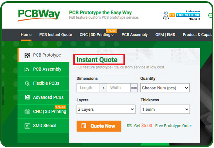
After writing the parameters in the given space, when you click the “Quote now” option you will come across the following page.
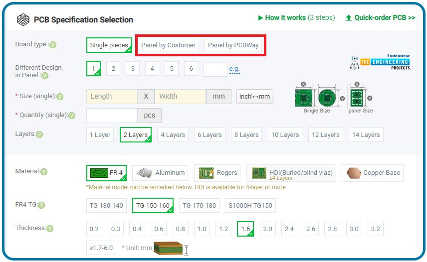
You can the option “Board Type” which is further divided into three categories with two options for PCB Panel. Either you can select the PCB panel by selecting the “Panel by Customer” option or you can ask PCBWAY to make the panel by selecting “Panel by PCBWAY”
You can select the size, quantity, number of layers, material, thickness and much more. Additionally, you can write down your further requirements in the “other special request” option. The primary aim is to give clear instructions so the final product exactly matches what you ordered in the first place.
Order Status
Once you submit the order, it exhibits full detail on how your order is going to be processed, including order status, address, past orders, invoice details and the total time it’ll take to complete the order. There are no hidden charges, which means you’ll be charged exactly the price you’ll see in the order status. Plus, if you find any difficulty in placing the order or in the selection of the material, they will guide you to make the final decision.
Live Chat Option
The website comes with a live chat option through which you can communicate with the agent for any query. Though their English is not impeccable, but it still good enough to understand your questions and answer them properly. You can contact them any time from Monday to Friday, however, if you want to contact on the weekend, you can submit your email address and leave a message and they will get back to you within one business day.
Quality Assurance
Once the boards are manufactured, they go through a rigorous inspection test to ensure the quality of the product. This includes if the holes are properly drilled and aligned, the uniformity of the traces all the way through the board, and a thorough comparison with the design document to ensure that all the requirements are met. The inspection tools include an X-ray inspection machine, a flying probe tester, and an automated inspection machine. With 50 engineers on board, rest assured the final product gets the proper treatment it deserves.
Final Thoughts
As mentioned earlier, panels are used to produce PCBs in bulk. Moreover, they also refrain the boards from vibration and shock during the assembly process.
A simple coordination between the PCB designer and Panel designer can help build the PCB panels with accuracy and efficiency.
If you’re a newbie and just starting out, it’s better to get your PCB manufactured by the professionals in the PCB fabrication house. This will save you both time and money and you’ll learn many things along the process.
That’s all for today. Hope you find this article helpful. If you have any questions, you can ask me in the section below. I’d love to help you the best way I can. Thank you for reading the article.


