JLCPCB (JiaLiChuang Co. Limited) is a worldwide PCB & PCBA Fabrication enterprise. It is a leading company in high-tech manufacturing products specializing in PCB and PCBA production. With over a decade of experience in PCB manufacturing JLCPCB has made over a million customers through online ordering by the customers of PCB manufacturing and PCBA production.
JLCPCB is a professional manufacturer of large-scale manufacturing of PCBs, well equipment, strict management, and superior quality. It deals with the production of all types of PCBs, Stencils, and SMT.

In this article, we are going to discuss widely how the company operates its ordering system of the PCBs by their customers for production through the online booking process.
JLCPCB SMT Services
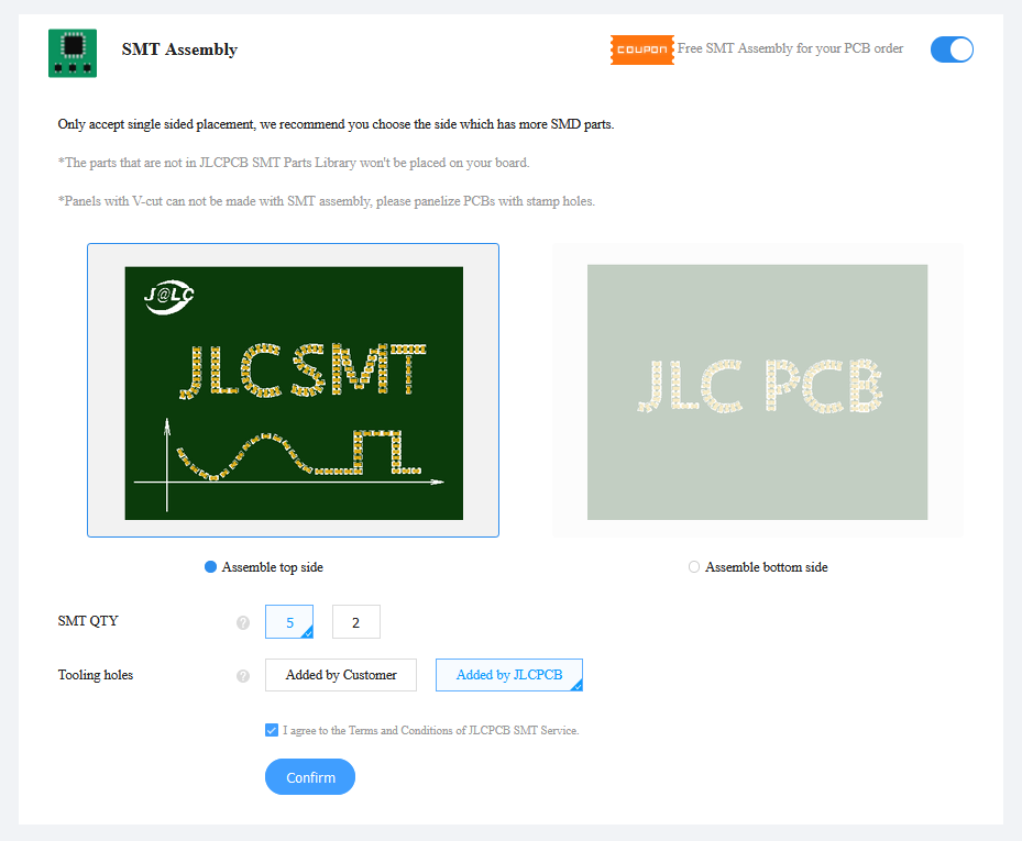
Normally, SMT components are used in professional/industrial PCBs and JLCPCB offers the best SMT services. You should first check these JLCPCB SMT services to get an idea. Let me highlight its important points:
- JLCPCB offers single-sided placement on the PCB board.
- JLCPCB has an extensive Library for SMT parts and you need to select the components from there.
- JLCPCB manufacture SMT Components in-house and thus gives the best results.
- JLCPCB places automated solder paste and then performs Solder Paste Inspection(SPI).
- I have attached the SMT Assembly screenshot in the below figure:
So, it's quite easy to order for manufacturing of Metal Core PCB on JLCPCB.
How to place an order online
Ordering of PCB at JLCPCB is not a complicated process, since the system is user-friendly to every customer. The steps below show the steps to be followed when placing an order.
STEP 1:
Register on the official site of JLCPCB, if you don’t have an account. if you already have an account just log in

STEP 2:
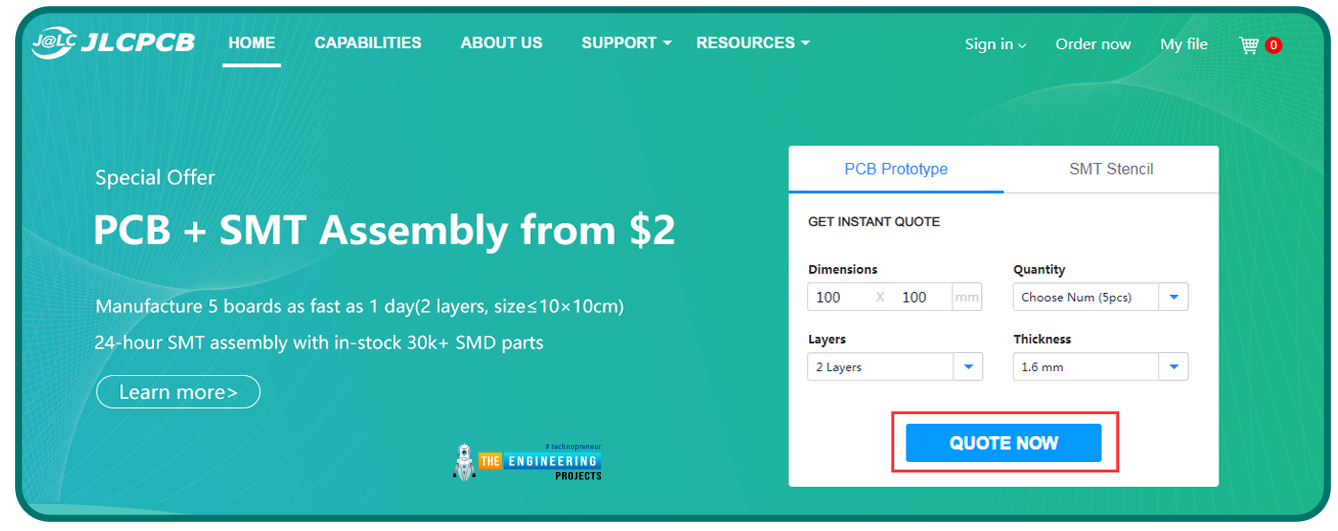
After login into one account. It will display a home page with a quotation calendar that will display an ordering page. On the quotation calendar, the customer would be asked to enter the size of PCB which he/she requires, quantity, layers, and thickness of their choice
STEP 3:
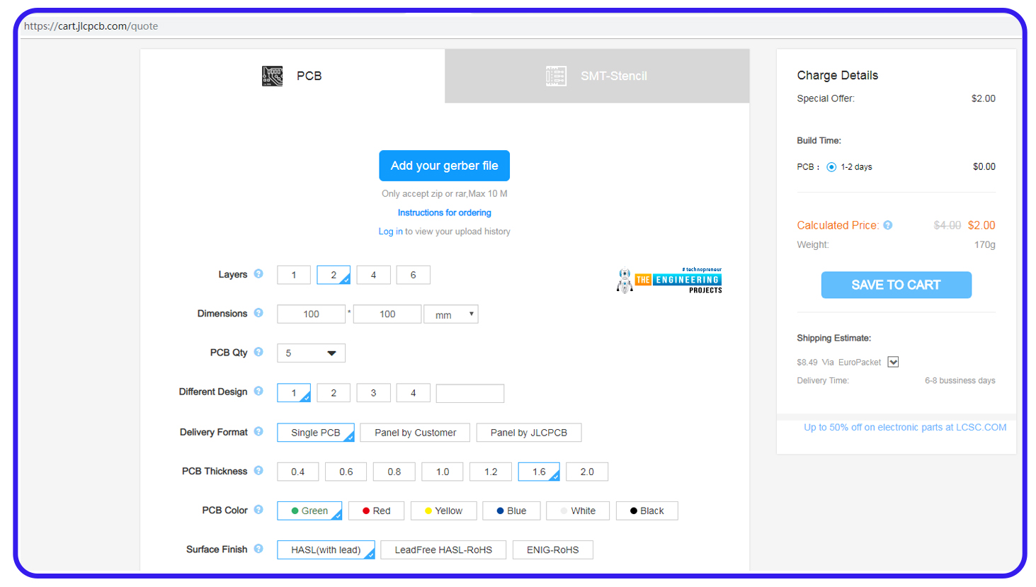
In this step, the customer is required to enter the PCB board details on the online calculator to get the price of the quoted items in step 2. Also, there is the minimum price which is the cheapest one for a particular PCB.
STEP 4:
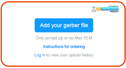
Then click to “Add your Gerber file” this will upload the file. There are written guidelines on how to generate different Gerber files in the best format on the well-known circuit design program found in the company industry. A very small customer ID is always added to the PCB ordered to distinguish the PCB order from all others.
If one wants to put it in a specific location you are required to indicate the location by adding a unique text like “PBCJLPBCJL”
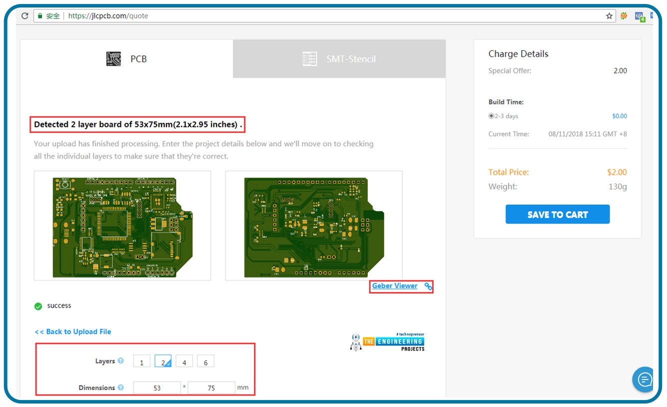
The system will analyze the file Gerber to confirm the dimensions and layers of the board after uploading the Gerber file.
STEP 5:
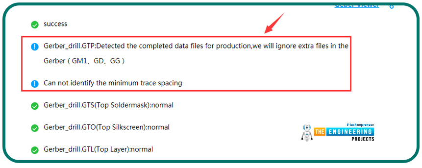
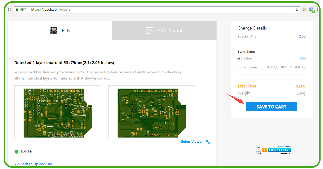
Then click the “Gerber viewer” to the design of the boards. Customers are advised to confirm the Gerber file carefully for any errors. After checking and confirming the errors and no problem is detected just click “save to cart” and continue to the next step
STEP 6:
After saving to cart then click “add new item” if you want to order multiple PCBs repeat the same steps from the beginning as you add both of them to the cart.
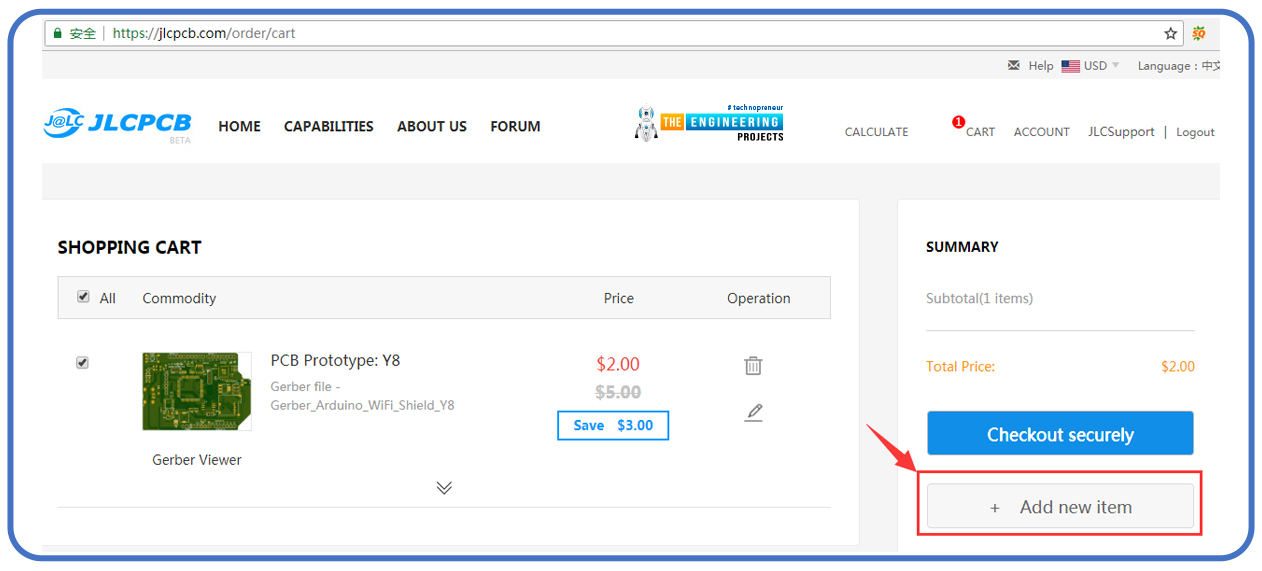
STEP 7:
Expand the cart and view all the details of the PCBs ordered, including the price of each one of them, its specifications, and all the number of PCBs ordered.
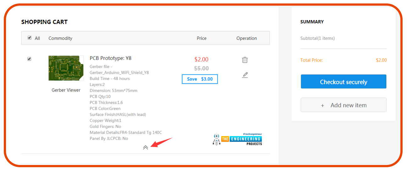
STEP 8:
After viewing all the details in the cart and seeing all the PCBs you wanted click the “checkout securely” button

STEP 9:
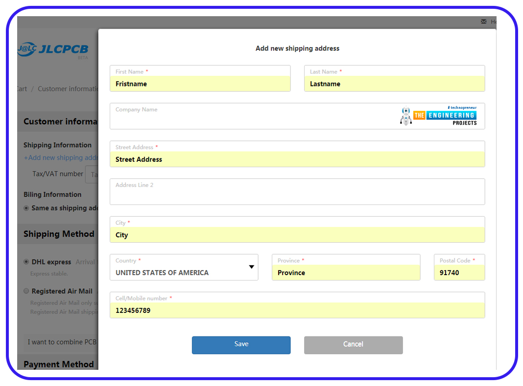
On the checkout, menu add your shipping address where are the PCBs are to be shipped. The country where the PCBs are shipped determines the rates. Also, the shipping options are found on the same page just below the address. The shipping methods available are DHL and Airmail both of them vary in their delivery time.
This is the payment method. JLCPCB offers two kinds of payment methods which include
- Pay directly: this is the most recommended method of payment by the company. It is recommended since it ensures the high efficiency of manufacturing. If the customer file hasn’t been reviewed for production you will get a refund.
- Review before payment: one can pay after the file has been approved. In this method, the design will not be produced until payment is made. Results of the review will be made through email. It is recommended to pay as soon as the file is approved to avoid delivery delays. When the file is not approved the order is automatically canceled.
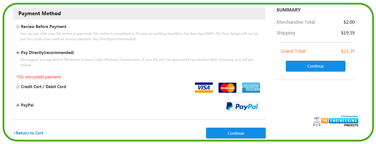
When the order payment is made the company arranges the production where you can go through your “ACCOUNT” menu to track your order status.
Adding a new order to your existing order
Customers may sometimes feel the urge to add a new order to the existing order. This may be because may feel the items ordered are not enough or an increase in demand for the PCBs which were previously ordered
Here below we are going to go through the steps of how to add a new order to the existing order in JLCPCB.
STEP 1: log in to your account and locate the existing order.
When you log in the process will only go through if the existing order is still in the production process. If the order is finished and delivered you will not be allowed to add an order unless you make a fresh order.
STEP 2: You will open the ordering page, upload the Gerber file and add the items you want and click “combine”. Also, this will only appear if there is an extra shipping cost for the order added.
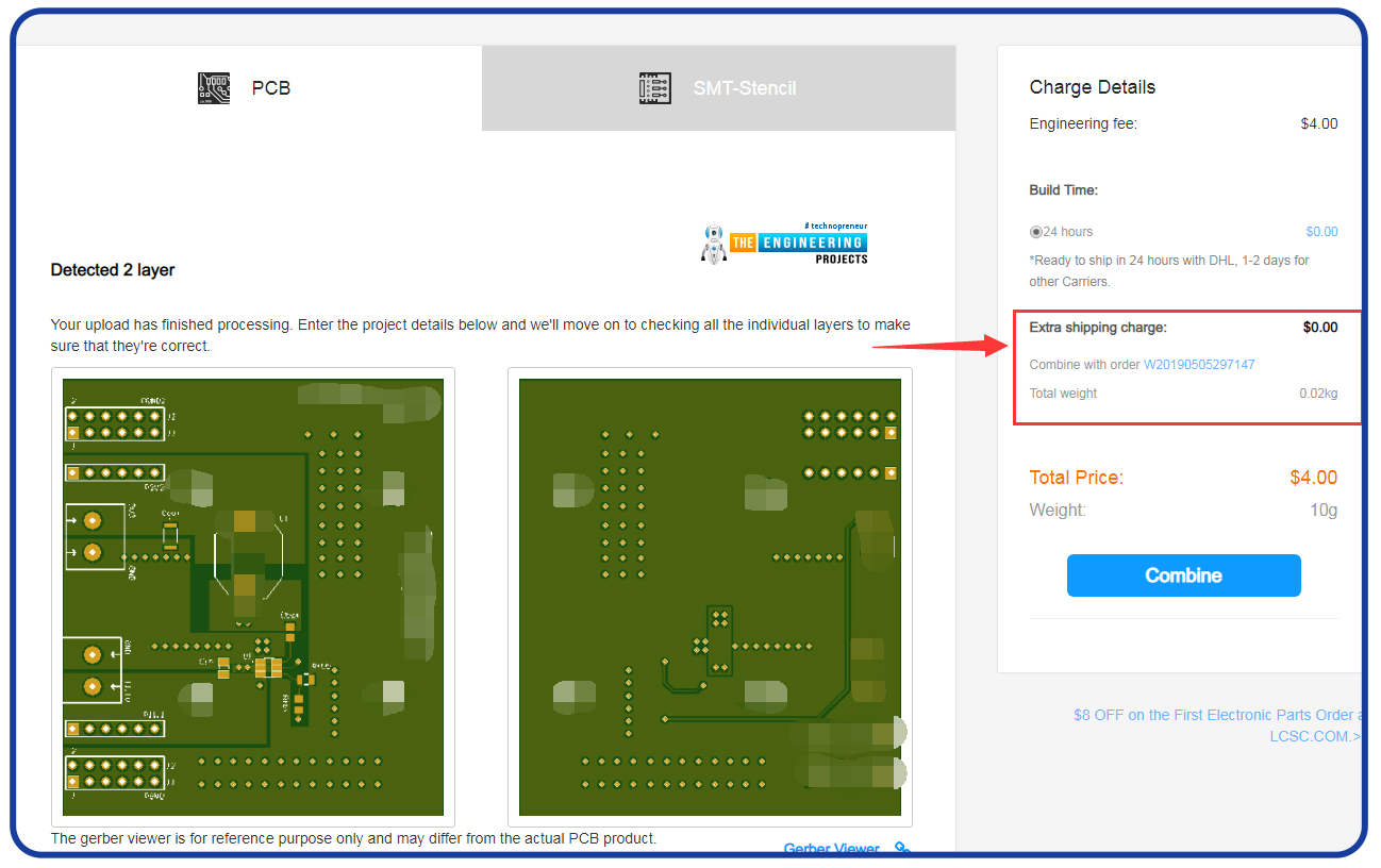
STEP 3: when you click “combine” a new order will be added to the existing order and you can check on its progress.
How to track your orders
After placing your order and payment has been made successfully, you can track your order through your account on the company website. Let’s discuss the steps to track your orders.
STEP 1: Open your order history
Login to your account and account menu click order history. After clicking on order history it will direct you to a previously placed orders page where all your previous orders are listed indicating their current status
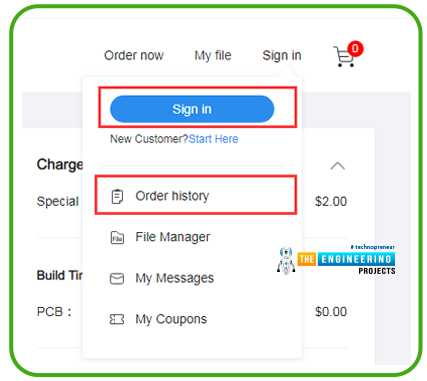
STEP 2: Check your order status
Once you open the product files column file review status will appear and also the order status in the order status column. Then click order details to learn more.
STEP 3: Track production process
When you are put I am production-ready to be processed. Click the production progress to check the process.
STEP 4: Track shipment status
Once the order has been put into production and processed shipment process takes place. Once the shipment process has started a shipment notification will be sent through your email advising you on the shipment status of your order and the shipping tracking number. One can also use the JLCPCB company website to track the parcel. While on the website click shipment tracking and all the details about your parcel and delivery time information will be displayed.
Instructions for ordering PCBs from JLCPCB
Some users experience confusion during the online ordering placement of the PCBs from the company. Below are instructions on some routine internal actions JLCPCB will make when they receive the order.PCB file and Gerber file in the zip file at the same time
A Gerber file is a file containing the format of the printed circuit design which is used in the fabrication of data. So while ordering the printed circuit boards on your account if both Gerber files and PCB files are in your zip file, the system will follow the Gerber file and reject the PCB file.Solder resistance bridges
When the person ordering the PCBs does not specify on the solder mask bridge which is importantly required, it will be ignored. When doing the solder-resistance bridge a spacing between the pins needs to be 0.254mm and special notes on doing that are required.
The English description and the attachments on the zip file
Zip file attachments such as PDF files, EXCEL, DXF files, etc are ignored and PCB will be done according to the Gerber file provided. One should ensure the correct parameters are chosen and those needed to be converted into a Gerber file when placing your order. If otherwise, zip files attachment are important should be added to the remark field.
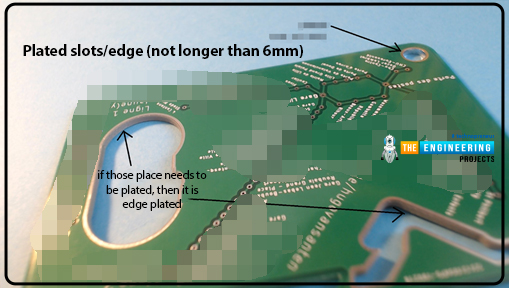
Plated slots/edge (not longer than 6mm)
In the presence of plated slot or edge, they should not be longer than 6mm, and make a note about it when placing the order or the system will make it for you. In the case where no note is provided the company will assume it and make it in the normal process.
Software incompatible issues
Since there is the use of different software by different clients to design the printed circuit board and the software where Gerber data is processed is not the same as the software used in designing the data it sometimes causes the software incompatibility problems to appear. Due to the reason of no warning notification when transferring and importing the data into the software so it is not easily noticeable and cannot be confirmed to the customers. This makes the company responsible for some of the problems caused by software incompatibility.
Markings on base materials
There are some marking that sometimes appears on the base material. This is because of some security issues and there is a way it can be removed. There is no track on which PCB will have the mark so all the PCBs have equal chances of having the marks. One should check from their side whether it is accepted while placing the order.
Gerberview
This tab is functional for reasons of reviewing the file quickly before paying for the order. Acts as the preview button on the website. At times the website causes errors when there is something wrong to display it exactly so it is advisable before placing the order to check the file carefully when you feel there is doubt.
Design about slots/v-cut/cut out/millings
The customer should ensure the v-cut line, cut out and millings are located on the same layer with the board outline. If not on the same layer with the board line it will not appear. It is advised when one is placing the order should check carefully because when it is missed due they are not in the same layer with the board outline the company will not be responsible.
Silkscreen/text
When you want the silkscreen clear on the PCB board the width of the texts and space between letters should not be less than 0.15mm and a width of not less than 1mm. when outline is the font is made and the solid part is filled with lines the fillings then should not be less than 0.15mm. the company will not modify the silkscreen on the Gerber file but the text may be widened. If the text is not enough the company will not be responsible for any complaints made regarding unclear texts caused by nonstandard design.
Layer PCB
JLCPCB company does not make 3 layer PCBs. If one orders a 4 layer PCB with a single inner layer, the company will process it with the 4 layer process directly and confirm with the customer again. So before placing an order confirm whether there is an inner layer miss or not.
Repeat order
This is the placing of orders same just as the previous one which had been successfully processed. With these orders, the company will not make any changes to the file which was used in the production. The customer should ensure not to leave any related note for the order to be changed while placing the order since the repeated order will not be checked manually by the engineers.
Items found on the board outline
The board outline is used to show how the PCB will look like when made. So everything that needs to be included in the board should be cut out clearly on the board outline. You should avoid the least useful items to avoid confusion. When both the GKO layer and the GM1 layer are found on the Gerber file the engineers will ignore the GKO layer and make boards according to the GM1 layer. when GMI, GM2 or GM2, GM3, GM4 layers are in the Gerber file at the same time, engineers will go for the smallest number after the letter GM as the outline layer by default.
JLCPCB panel
When you place an order to JLCPCB the JLCPCB panel will panel the order by default with the v-cut. JLCPCB only panels PCBs with rectangular and circle shapes. When you penalize the boards yourself but choose “Single PCB” when ordering, the numbers of designs/boards in the Gerber file should not be greater than 5, otherwise, we may cancel this order. If “Panel by Customer” has been chosen, the designs in the panelized Gerber file should not be greater than 10.
The remark field
The remark field is used when you place your order so that you can leave a note in case of any import, but the company does not recommend the use of this option since all the orders with an English note will take a longer time to get through the audition process.
Board larger than 200mm*250mm
Large boards sometimes the company might consider them, but if the good board available can not meet the quantity like the one ordered on the website due to the high cost of production they will ship the good boards and refund the difference to you.
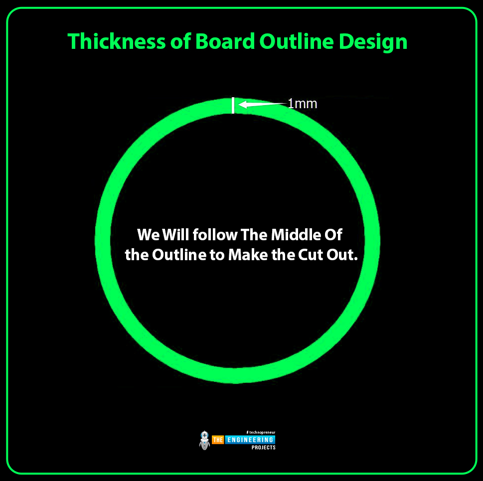
Thickness of board outline design
The recommended thickness design of boards outlined by the company is 0.15mm. in a case when the board is greater than 0.15mm the centerline will be followed to make the board outline
Order cancellation
Orders missing crucial information such as the board outline, solder mask layer the order will be canceled out clearly during the audit process.
Orders beyond company capabilities
Orders beyond the company and engineers’ capabilities, will be canceled directly and an email will be sent to inform you about the reason. So before placing an order kindly check your file carefully before you pay for the order to save the loss due to the cancellation.
Removal of the order number
Order removal will not affect the functions of the boards if JLCPCB puts the order number at random or miss to remove. The removal of the order number will be refunded.
Easyeda generated file
Easyeda is a free online tool that we provide to design the PCB, and you can place your order on JLCPCB easily and quickly. But if there is a manufacturer error due to the design error, we may not responsible for that.
Silkscreen and solder mask openings
When the silkscreen overlaps with the openings on the board surface, the principle of openings first will be put into consideration. we will ignore the silkscreen and make the openings on the boards only. In the case where you want to keep the silkscreen on the openings, kindly make a note in the remark column so that the company engineers and factories pay attention to it and meet the required standards.
How to order PCB boards with solder mask defined pads
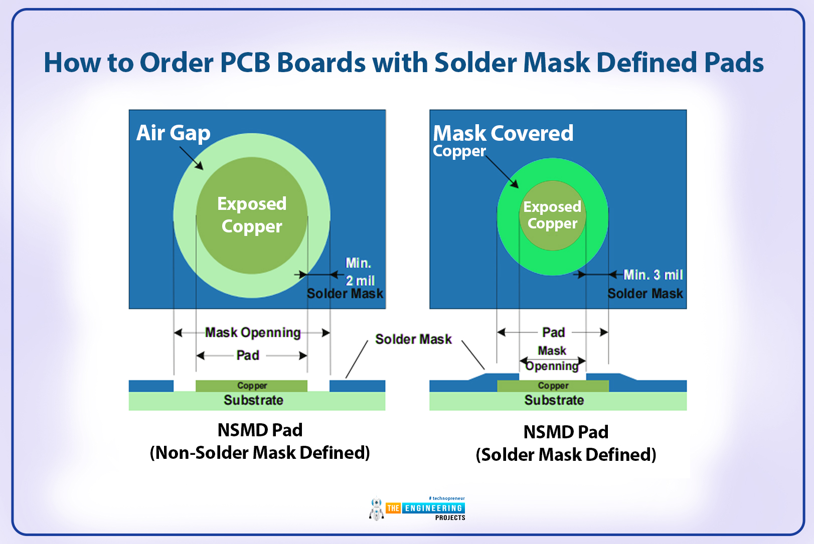
solder mask clearance is larger than the copper pad it’s exposing, in most PCBs, these pads are known as Non-Solder Mask Defined pads (NSMD).
Some of the other components have another type of solder mask called Solder Mask Defined pad. Which has a clearance of solder mask that is smaller than the copper pad. One can suggest pad and solder mask clearance size in the datasheet when applying. One should ensure that at least 3 mils (0.076mm) of the mask will be printed on all sides of the copper pad. The reason is registration tolerance on the solder mask placement if the mask is smaller than the pad there are possibilities that the mask could move enough exposing bare substrate which will lead to bad results.
How to transfer SMD INFORMATION TO JLCPCB
In the ordering system, there is no given option to add details on whether the board required has an SMD pad. If CAM engineers don’t get this kind of information the solder mask clearance for SMD pads will be enlarged to its default size.
When transferring SMD information to JLCPCB the following steps are used
Write a special instruction
On your account page in the ordering system, there is a text box called “PCB Remark”
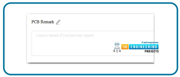
Write a special instruction informing JLCPCB that your order design has an SMD pad
Confirm production file
After writhing the special instruction on the Remark box select “yes” for the “confirm production file” option
On clicking yes, the JLCPCB engineers will come up with a production file that is required to manufacture the PCB. When the production is put into consideration a check notification will appear where you can check and confirm it before reproduction. An email will be sent to you when the file is complete and ready for production. Download the processed Gerbers, pay attention to inspect the solder mask clearance for the SMD pads
Benefits of the ordering PCBs from JLCPCB
- Higher quality: JLCPCB has advanced its production technology by providing high precision boards suitable for industrial, military, and medical applications.
- Low cost: the company’s mission is to efficiently increase its production of PCB board at a lower cost. JLCPCB produces the cheapest but most efficient PCBs possibly because of extremely high production efficiency, and less human resource cost.
- Fast delivery and user-friendly online ordering platform: the easy online ordering process have led the company to be a leading manufacturer of PCB with efficient and professional customer service, digital technology used in manufacturing, automatic production lines
and their able logistics partners make every step to deliver your PCBs faster.
- Shorten turn around time: PCB prototypes can be made faster even within 24hours because of the automated equipment and the fast technology we utilize the available capacity of our factories network so that system can match your orders to one of our factories which is best suited, in the shortest turnaround time.
Conclusion
JLCPCB is a good company since it provides great customer satisfaction, as long as you consider the time differences, and try to make orders with enough time to respond during your working days, and making orders, not near the weekend, they are well worth the money saved and the simple interface.
Their chat support is fairly good, and the assembly service is also mostly good.


