Hello friends, I hope you all are doing great. Today, I am going to share the 10th chapter in the PCB learning series. So far, we have studied the basics of PCB i.e. What is PCB? Main Types of PCB, techniques to mount components on PCB etc. Now, we are ready to have a look at the complete PCB Fabrication Process.
So, in today's tutorial, I am going to share a detailed guide on PCB Fabrication Process. We will discuss everything related to it i.e. How PCB boards are manufactured? Which material is used to fabricate printed circuit boards? etc. But before starting the Fabrication PRocess, we first have to understand a few terms/features. So, let's get started:
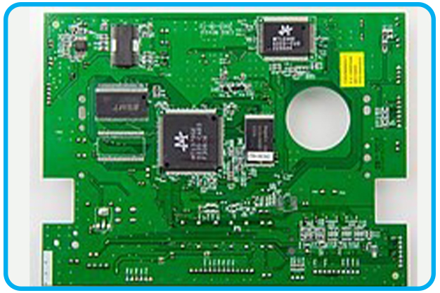
- PCB of DVD player:
RoHS-compliant PCB
- RoHS stands for Restriction of Hazardous Substances.
- EU ban the use of lead under the legislation RoHS. So, in PCBs, lead can't be used.
- RoHS-compliant PCB means that PCB is free from lead, Mercury and other heavy toxic metals.
PCB Lamination
- Laminates are prepared, first controlling pressure and temperature for cloth or paper with a thermoset resin and then a final integral piece of uniform thickness is formed.
- Its size can be up to 4×8 feet.
- Desired thickness can be achieved by controlling cloth weaves, thickness and resin percentage.
- Some important characteristics of the laminate are:
- strength of fire retardant
- dielectric constant(e) of the laminate
- the loss factor of laminate
- tensile and shear strength of the laminate
- the glass transmission temperature and
- the z-axis expansion coefficient.
- Polytetrafluoroethylene(Teflon)
- FR-1, FR-2, FR-3, FR-4, FR-5,and FR-6
- CEM-1, CEM-2, CEM-3, CEM-4, andCEM-5.
Here are a few of the factors affecting the laminate quality:
- Size of the board.
- Increasing frequencies.
- Uneven distribution of fiberglass glass or other filler.
- Bubbles and thickness variation in resin.
- Variations in the dielectric constant.
Key Substrate parameters
- The circuit board substrates are made up of dielectric composite materials.
- The composites contain
- matrix(epoxy resin)
- reinforcement(glass fibers, paper etc.)
- filler (ceramics)
- woven: these are cheaper but have a high dielectric constant that is not suitable for many applications.
- non-woven: these are expensive but suitable for RF and analog applications.
Key parameters of substrates are:
- thermomechanical(tensile and shear strength, glass transition temperature and thermal expansion)
- electrical(tracking resistance, dielectric constant, dielectric strength, breakdown voltage etc.)
- others(moisture absorption)
- At a transition temperature, thermal expansion increases because the resin in the composite becomes soft. Below transition temperature, thermal expansion decreases and matches with copper and glass. Above transition temperature, a very high thermal expansion exerts mechanical overload on the board components.
- Expositions to high temperatures and repeated soldering can be the reason for the failure of the plating, especially with thick boards.
- Dielectric substrate constant depends upon the material used and the frequency(decreases with the increase in frequency). Signal propagation speed depends upon dielectric and phase distortion depends upon frequency. So flat dielectric constant vs characteristics frequency is important. The transmission line impedance is inversely proportional to the frequency therefore faster edges of signals reflect more than the lower edges of the signal.
- At maximum voltage gradient, material suffers from breakdown is determined through dielectric breakdown voltage.
- Tracking resistance means how the material resists high-voltage electrical discharges creeping over the surface of the board.
- The amount of electromagnetic energy from the signals in the conductor, that is absorbed in the board material is called loss tangent. It is important for high frequencies. The cost of the board increases by choosing low-loss material(expensive) in high-frequency digital design.
- When the material is exposed to high humidity or water, moisture absorption occurs. Both resin and reinforcement absorb water. Absorbed water can cause degradation of key parameters. It affects tracking resistance, dielectric parameters and dielectric constant. Absorbed water can cause cracks during heating and soldering.
Common Substrates
- FR-2, FR-4, aluminum or insulated metal substrate( IMS) and flexible substrates(Kapton and parallax) are the commonly used materials as the substrate.
- FR-1, FR-3, FR-5, FR-6, G-10, G-11, CEM-1, CEM-2, CEM-3, CEM-4, CEM-5, PTFE(Teflon), RF-35, alumina and polyimide are rarely used as a substrate.
Copper thickness
- Copper thickness is the weight of copper per area. Its unit is ounce/square foot. (1 ounce/ square foot = 34 micrometers thickness).
- A heavy copper layer means 3 ounces of copper per foot. It is used for high currents and to dissipate heat.
- In FR-4 substrate 1oz copper/feet is the common thickness. Other options are also available.
- Metal core boards use thicker copper(35 micrometers) for high-power devices.
PCB Circuit properties
- Trace is made up of a flat but narrow copper foil and its resistance should be low. Its resistance is determined by its length, width, and thickness.
- In multilayer PCB, one layer is made up of solid copper that is used for power and shielding return.
- In microwave circuits, to attain consistent impedance stripping or microstrips of transmission lines are used.
- HDI PCBs have vias or tracks with a diameter of under 152 × 10^6 m.
Safety measurements
Some safety measurements should be considered, i.e.- flammability
- electrical tracking
- maximum operating temperature
- heat deflection
Old Technique for PCB Manufacturing
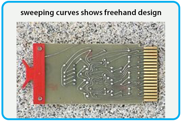
In the beginning, PCBs are designed on a clear mylar sheet having a photomask.
- First, component pins/pads are laid out on the mylar and then traces are routed to connect with the pads.
- Self-adhesive tape is used to make traces.
- In mylar layout, pre-printed non-reproducing grids are used.
- The final photomask is produced onto blank copper-clad boards having photoresist coating using a photolithographic technique.
Modern PCBs are produced by adopting the following steps.
PCB Fabrication Process
PCB manufacturing consists of many complex steps.
1. PCB Computer-aided Design(CAD):
- CAD software are used to create the software image of the PCB design.
- Commonly used PCB design software are Eagle, Altium Designer, OrCAD, KiCAD, Proteus etc.
- Online CAD software are also available i.e. EasyEDA.
-
Once the design is finalized, the CAD software generates the Gerber files, which include detailed information about drill drawings, copper tracking layers, component notations apertures, components labeling etc.
2 Panelization:
- Panelization is the process of adding a PCB design multiple times in a single PCB board.
- If you want mass production, the best practice is to create a panel of your PCB design.
- It reduces the cost and manufacturing time. (We will cover PCB panelization in our next chapter)
3 Copper Pattern Printing
- On the copper foil layer, the PCB design generated from CAD software is printed using black ink, it acts as a
protective mask for the copper under design traces/pads.
- The remaining unwanted copper has no black ink and a process called etching removes it, as it's unprotected by the design mask.
- Some other techniques used to create copper patterns:
- Silkscreen printing
- Photoengraving
- PCB milling
- Laser resist ablation
- Laser etching
4 Chemical etching:
- The process of submerging the board into the ferric chloride solution is called chemical etching.
- The function of etching is to remove copper from all the surfaces not protected by the resist.
5 Lamination:
- Note the via, visible as a bright copper-colored band running between the top and bottom layers of the board.
- A stack of material is laminated in a press by applying heat and pressure for a certain time. Multi-layer PCBs have trace layers inside the board.
6 Drilling:
- Drill bits are used to drill holes through PCB. It is made up of solid-coated tungsten carbide.
- Holes can be made conductive by electroplating. These conductive holes are used to electrically connect the layers of PCBs.
7 plating and coating:
- PCBs are plated with solder, tin or gold over nickel.
8 Solder Resist
- Areas that do not need to be soldered are covered with solder resistance.
9 legend printing:
- After the solder resists is done, a legend is printed on both sides of the PCB.
- Silkscreen printing, liquid photo imaging, and inkjet printing are the three methods to print legends on PCB.
10 Bare board test:
- Boards without components are tested for shorts and open. It is called the bare board test.
11 Assembly:
- Assembly is the process of stuffing bare boards with electrical components.
- After assembling, many tests are performed on the PCB. If it fails any test, means it needs rework.
12 Protection and Package
- For protection, a conformal coating is done to avoid leakage of current and corrosion.
- After all the protection checks, the final product is placed in a package.
Precautions
- Based on the required circuit, the PCB board dimensions are decided.
- Components and heat sinks are also positioned carefully.
- Decide the no of layers, ground and power planes as a power plane acts to encounter a ground plane, so shouldn't be together.
- Signal planes should be on external layers, especially if both AC and DC involve in the circuitry.
- High-frequency signals are routed in the internal layers between ground & power planes for attaining optimal EMI performance.
- Routes copper thickness, dielectric layer thickness and trace width are used to determine the line impedance. To route signals, normally three striplines are used named: microstrip, stripline and dual stripline.
- During components and vias placing on the PCB board, heat effects and geometry should be taken into account.
- If you are placing an order on a PCB manufacturing company, make sure you provide the final Gerber files.
How to order for PCB Manufacturing?
There are many online PCB Fabrication Houses available, offering PCB & PCBA manufacturing services. We are going to take the example of JLCPCB Fabrication House. Let's see How to place an online PCB Fabrication order on JLCPCB company.
- First of all, open the official website of JLCPCB Fabrication House.
- They have placed an online Quote Calculator, where you need to enter all your PCB requirements and it will give you the cost and time required to design it.
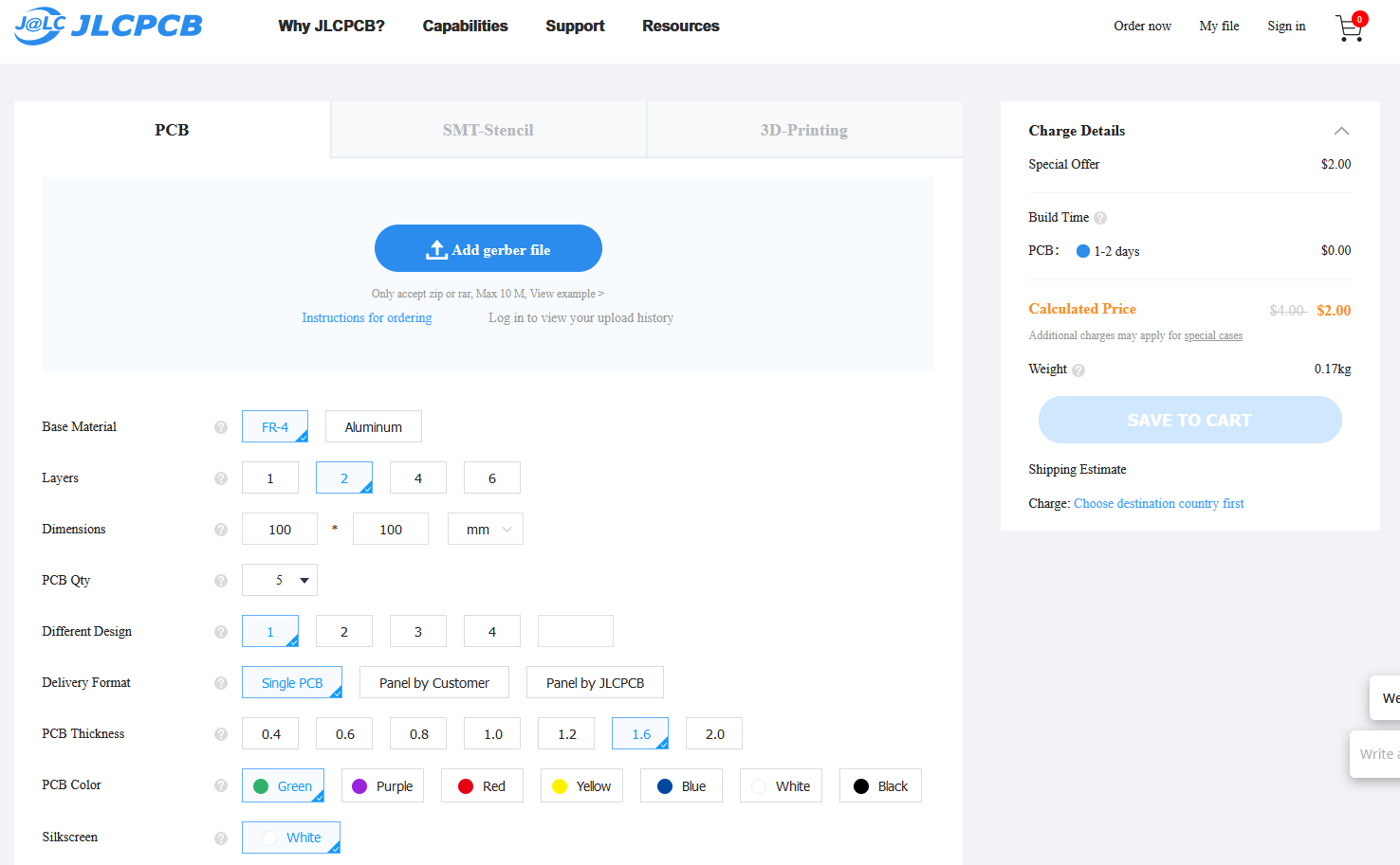
- As you can see in the above figure, I have placed an order of 5 PCBs and the size of each PCB is 100x100mm, and I am getting a price of $2.
- As you increase the quantity of PCB boards, the price per board reduces.
- JLCPCB is a well-renowned PCB Manufacturing House and always provides quality work at a nominal price.
APPLICATIONS OF PCB:
- In electronics: used in computers, home appliances, communication systems etc.
- In industry: used in power, measuring and industrial equipment.
- In medical: used in scanning, monitoring and surgery equipment.
- In the automotive industry: used in navigation, media devices, control systems and proximity monitors.
ADVANTAGES OF PCBs:
- Inexpensive/ cheaper.
- High volume production.
- Hold the components easily.
- Highly reliable.
- Automated soldering is possible.
So, that was all for today. In the next lecture, we will have a look at the PCB Panelization Process. I hope you have enjoyed today's lecture. Thanks for reading.


