Hello Friends! Hope you’re well. Today, I am going to share the 11th chapter in the PCB learning series. In today’s post, I’ll walk you through PCB Panelization, where we will discuss its definition, types, combinations, manufacturing guidelines etc.
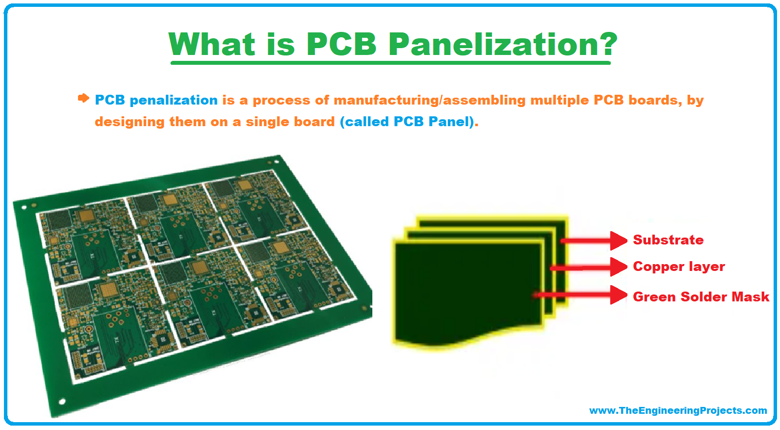
In PCB companies, CNC machines are used for PCB manufacturing and assembly. These CNC machines are capable of designing PCBs of quite large sizes. But normally, small-sized PCBs are used in electronic products. So, in order to fully utilize the power of CNC machines, PCB design is replicated multiple times(let’s say 10) and this final design is then fed to the CNC machine. This process of manufacturing multiple PCBs on a single board is called PCB Panelization and the final board created is called PCB Panel. A PCB Panel containing 6 PCB designs is shown in the below figure:
I hope you have understood the basic concepts, now let’s have a look at the definition of PCB Panelization:
PCB Panelization Definition
- PCB penalization is a process of manufacturing/assembling multiple PCB boards, by designing them on a single board (called PCB Panel).
- Once PCB Panel is manufactured, it is depenalized and separate PCB boards are plucked out of it.
- PCB Panelization is the most commonly used PCB manufacturing technique, as it saves both time and cost.
- If you have ever ordered any PCB then you must have the idea that as we increase the number of PCBs(to be manufactured), the cost reduces significantly, that’s because of PCB Panelization.
Why need PCB Panelization?
PCB Panelization is the most commonly used manufacturing technique because of its numerous advantages. Let’s have a look at a few scenarios, where PCB Panelization proves helpful:
Small Sized PCB
- If a small-sized PCB is manufactured on these CNC machines, the machine will consume almost the same power as that of a large-sized PCB.
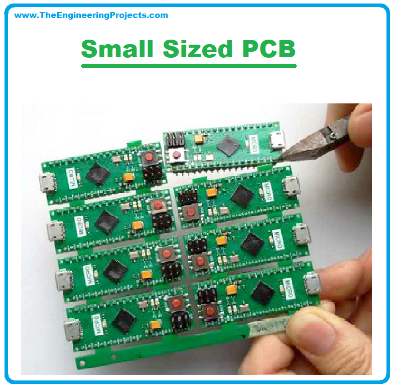
- So, if the PCB design(to be manufactured) is of small size, it is replicated over the panel and with a slight increase in the price, multiple designs are manufactured.
Product Designing
- In product designing, the PCB order normally ranges between 10k - 100k.
- In such cases, PCB Panelization is used to save time and cost.
Combinations of PCB Panelization
In PCB Panelization, we have three types of combinations, termed:
- AAAA Combination
- ABAB Combination
- ABCD Combination
1. AAAA Combination
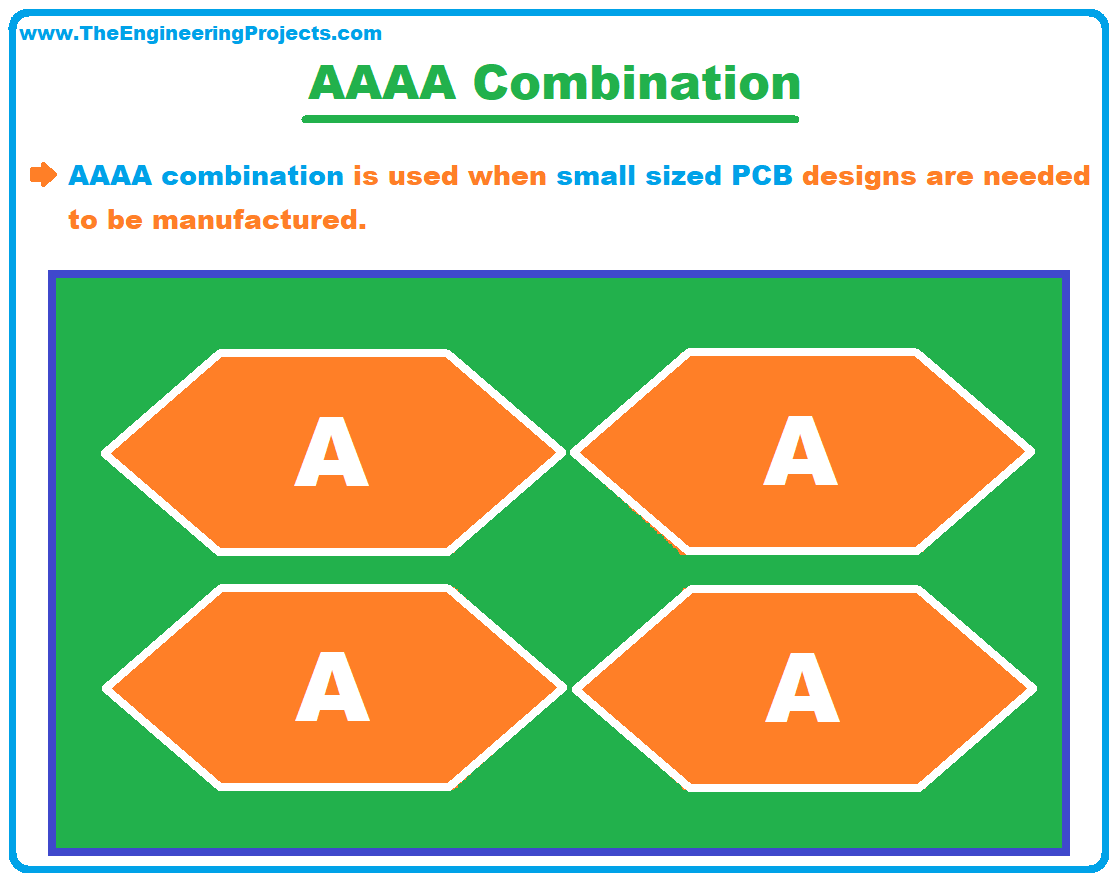
- In AAAA Combination, PCB Panel has identical PCB designs on it.
- This combination is used when small-sized PCB designs are needed to be manufactured.
- For example, a car locking RF remote has a single PCB in it as it's a very small product.
- So, the company manufacturing this product must be using PCB Panelization in AAAA Combination.
2. ABAB Combination
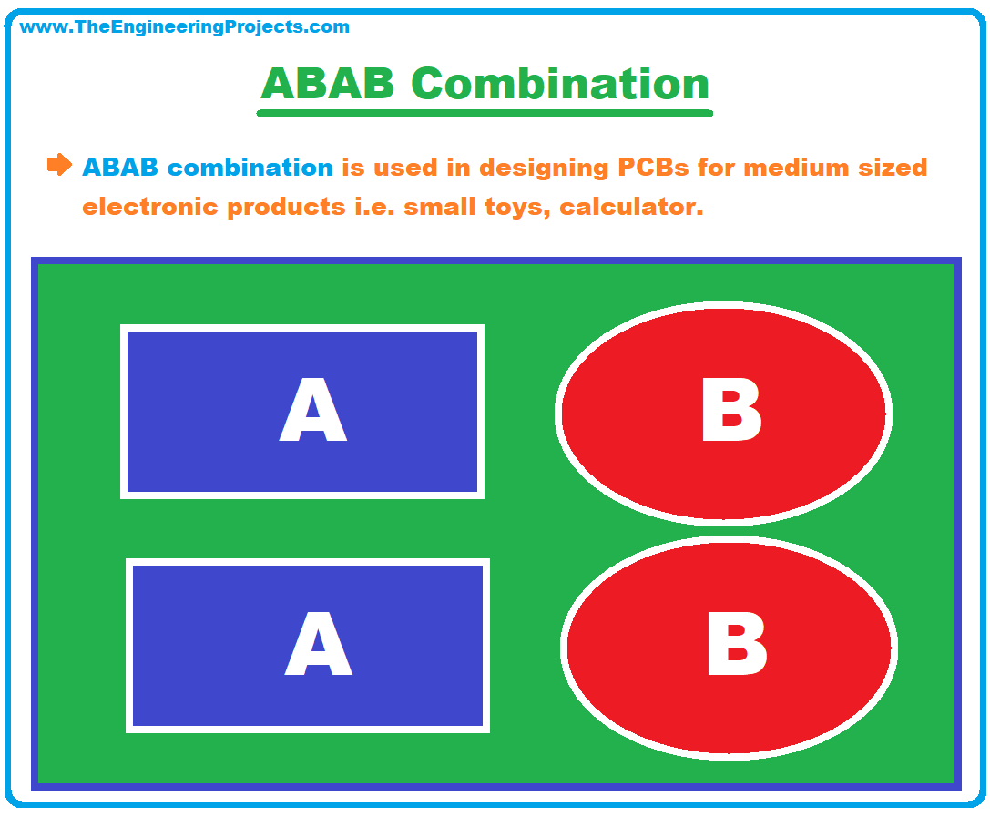
- This combination is used in designing PCBs for medium-sized electronic products i.e. small toys, calculators, handheld devices etc.
- In such products, around 3 to 5 small PCB designs are used, which are interfaced together in the final product.
- So, for designing multiple PCBs of a single product ABAB combination is used in PCB Panelization.
3. ABCD Panelization
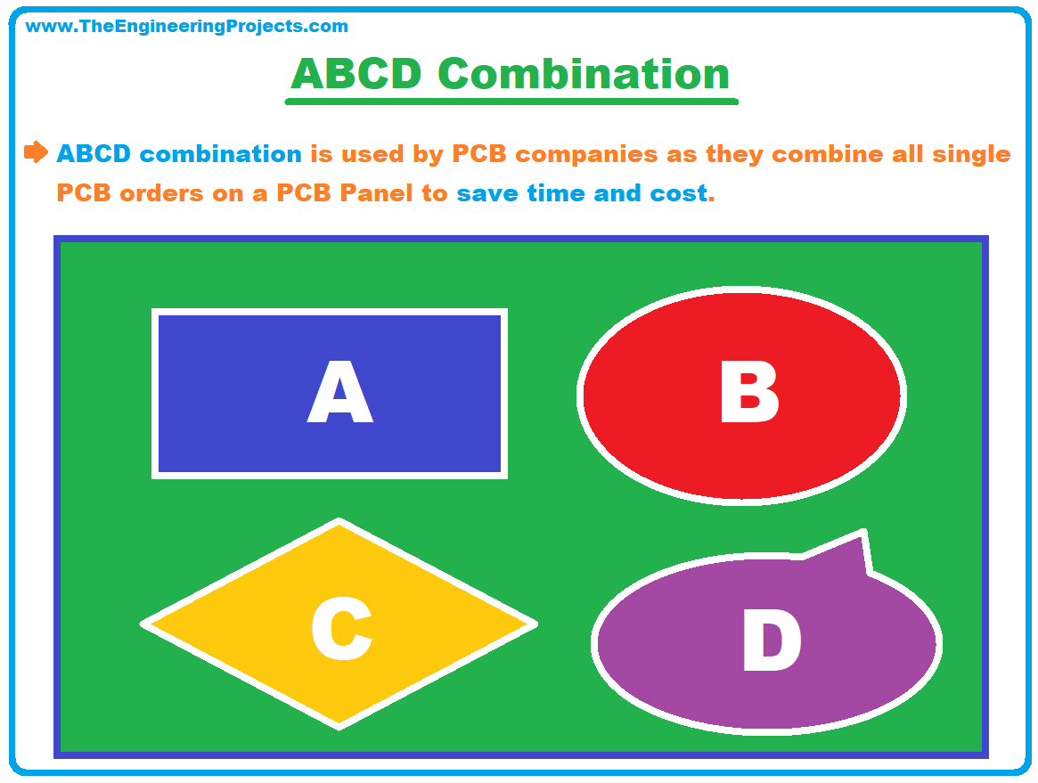
- In ABCD Combination, the PCB Panel has different PCB designs on it.
- This combination is normally used by PCB companies as they combine all single PCB orders on a PCB Panel to save time and cost.
- This combination is a bit tricky as it involves extra care for each PCB design.
Depanelization Methods:
- Depanelization is the method to remove the smaller PCB boards from a PCB Panel.
- Normally, two types of depanelization techniques are used, named:
- V-Scoring
- Tab Route
1. V-Scoring
- V-Scoring, also known as V-grooves, is a method of placing a straight-lined V-shaped groove between the PCB designs.
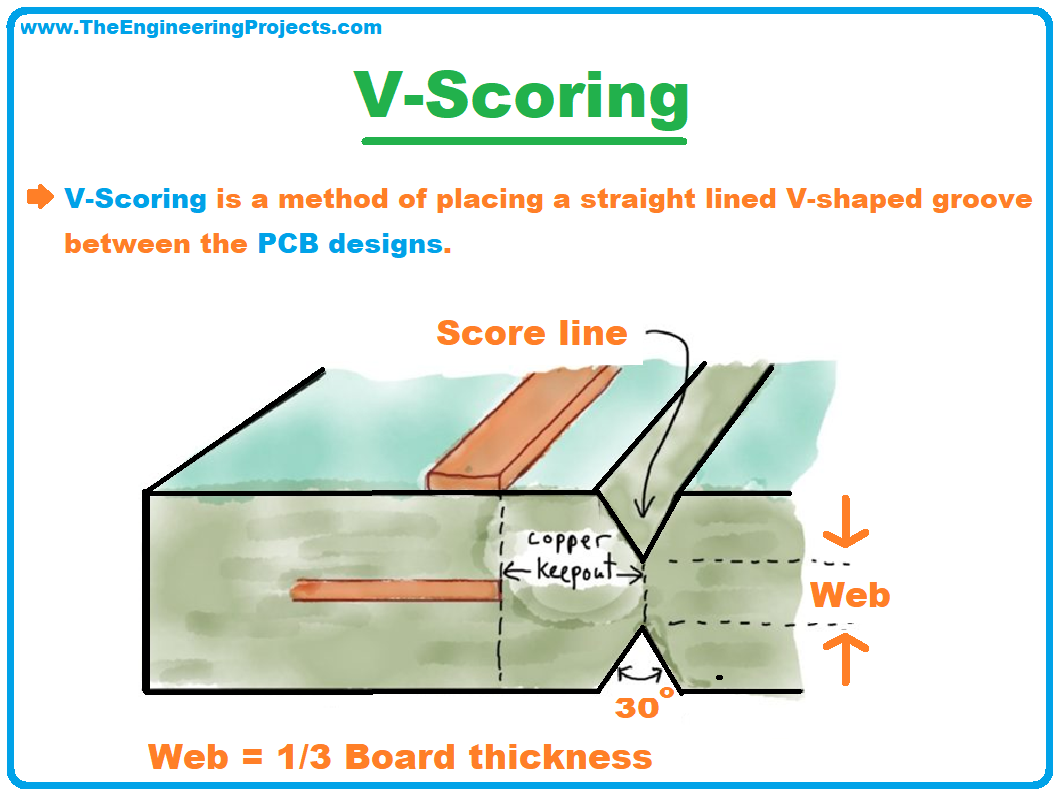
- While applying the V-grooves, it is important to create a cut of an equal depth i.e. 1/3 on the bottom and 1/3 on the top, making sure the middle part ‘the web’ remains connected.
- This method is useful for boards with regular shapes with sizes over 75mmx75mm.
- It is advised to use machines and fixtures to depanelize the boards, as manual removal can damage the components placed at the edge of the board.
- Know that the V-scoring is a continuous process and cannot be stopped in the panel, however, if you have multiple different boards to be depanelized, it’s better to use the following tab route method.
2. Tab Route
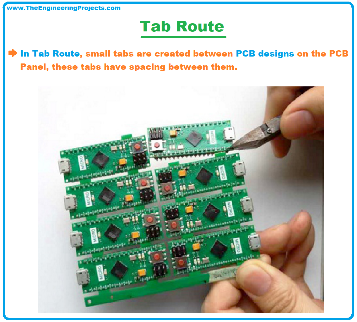
- In this method, small tabs are created between PCB designs on the PCB Panel, these tabs have spacing between them.
- This method is useful for the depanelization of ABCD combinations i.e. different circuit boards.
3. Breakaway Rail
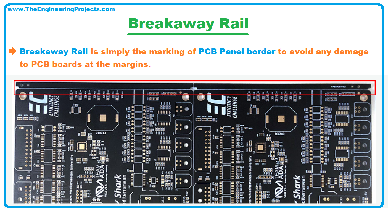
- Breakaway Rail, also called Edge Rail, is simply the marking of the PCB Panel border to avoid any damage to PCB boards at the margins.
- The Edge rail is simply removed during depanelization and both V-scoring or Tab Route could be used.
PCB Depaneling Technologies:
Now, let's have a look at the PCB Depaneling Technologies used to separate the individual PCB Boards from a PCB Panel. A few of these PCB Depaneling technologies are as follows:
- Pizza Cutter/V-Cut
- Water Jet Cutter
- Laser Cutter
- Router
- Saw
- Punch
- Hand Break
Pizza Cutter/V-Cut
Pizza Cutter is a rotary blade, with a motor. The Motor rotates the blade and PCB Panel is placed in front of the blade to cut into pieces.
Water Jet Cutter
Water Jet Cutters use a high-pressure stream of water to cut the PCB Panel. Abrasive particles are added to the water stream to make the cutting smooth. A water Jet cutter can be used for various PCB materials i.e. metal, aluminum etc.
Laser Cutter
A high Laser Beam is used to cut the PCB Panel into individual PCBs. Laser Cutting has high precision and accuracy as compared to any other method.
Types of PCB Panelization:
The four types of PCB Panelization include:-
Order Panelization
- To order panelization, a single PCB design is replicated all over the PCB Panel.
- This is the most common type of Panelization used in manufacturing industries.
- Though you may come across a few operating difficulties while using this Panelization, it doesn’t compromise the quality of the final product.
-
Rotation Panelization
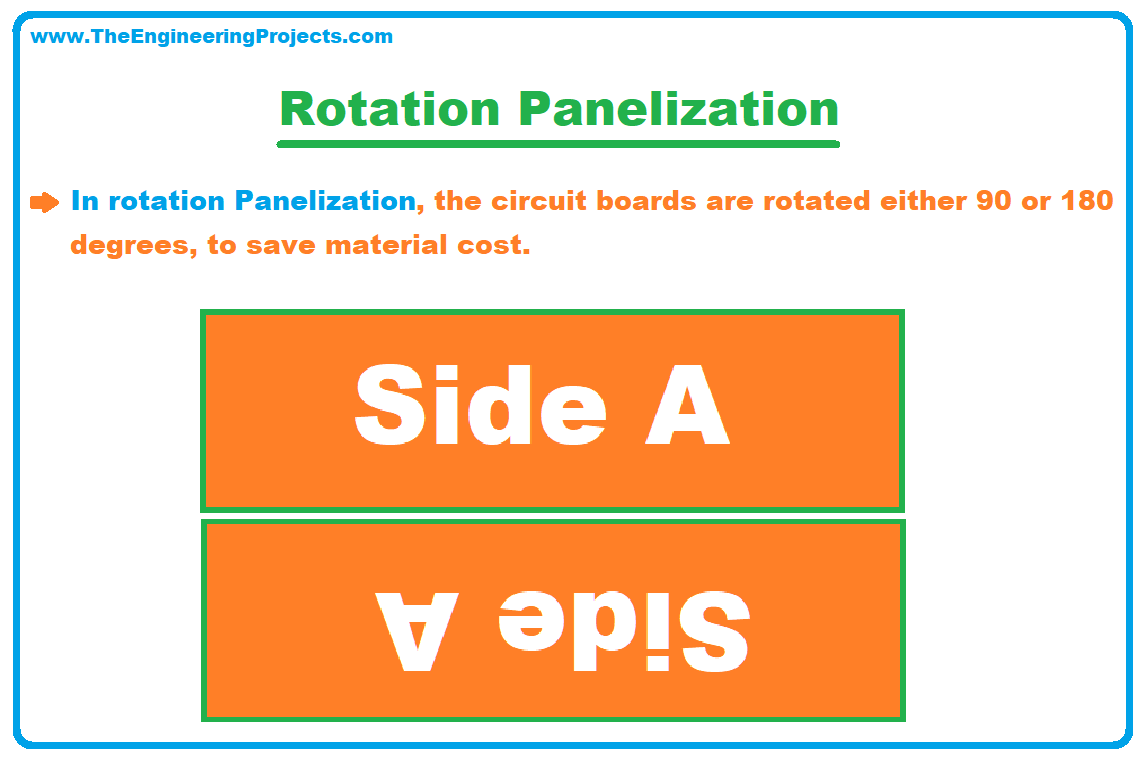
- In rotation Panelization, the circuit boards are rotated either 90 or 180 degrees, to save material cost.
- This panelization is normally used for designing irregularly shaped PCB designs.
- Suppose you are working on triangular-shaped PCB designs, then it would be the best practice to place the alternative one upside down, as shown in the below figure:
-
Combination Panelization
- Combination Panelization, also called characteristics Panelization, is a special type of Panelization that involves combining different types of circuit boards based on the combination principles.
- It is beneficial for designs containing different circuit board combinations in electronic units like toys and household appliances.
- We have already discussed those combinations i.e. AAAA, ABAB and ABCD.
Things to Consider for PCB Panelization
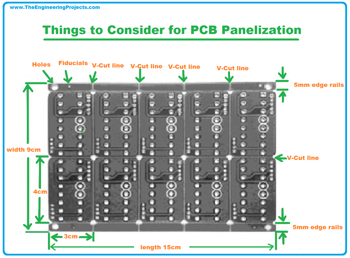
The following things you must consider during the PCB Panelization:
- Panel Size: Different manufacturers use different panel sizes. The panel size mainly depends on the size of the board you want to be manufactured. It is beneficial to work ahead with your PCB CM (a contract manufacturer) and ask about the Panel size of the manufacturing units. If necessary, you may need to alter the PCB size to accommodate the standard panel size.
- Layer Stackup: Not only multiple PCBs can be laid out on the panel, but Panelization ensures a cost-effective and efficient manufacturing process. And if you want to panelize multiple circuit boards, it is a good idea to keep identical layer stack-ups for all boards.
- Panel Structure: The circuit boards will usually require certain clearances to the edge of the panel and to each other and will generally come up with alignment holes. Again, coordinating with your CM can help you produce a final circuit board that can be effectively panelized.
- Panel Layout: The boards are placed to effectively use the space of the panel and the direction the board will take during the soldering process is a major concern. To effectively panelize the circuit boards, it is a good idea to work ahead with your CM to define the direction of the board through the soldering process.
- Breakouts: The panels are either depanelized with V-groove or with the routing method. The space you require between the components and the edges of the board is mainly dependent on the depanelized method you pick. The routing method requires 0.125 inches of space between the components and board edges while the V-groove method requires 0.075 inches. These board edge clearances keep the solder joints from major damage during depanelization of the board.
- Component Clearances: Components coming out of the board edge may require additional clearances based on the requirements of the manufacturing processes. If the components are large and overhang the edge, the clearances should be more than already defined for the V-groove and routing depanelization method.
- Panel Tooling: The board panels will require their own fiducial marks and tooling holes to resonate with what is on the circuit board.
- Physical Support: Different boards come with different thicknesses and sizes. Sometimes, additional support is required to keep the boards from sagging during the manufacturing process. To achieve this, a brace is included in the panel based on the board layout.
Advantages of PCB Panelization:
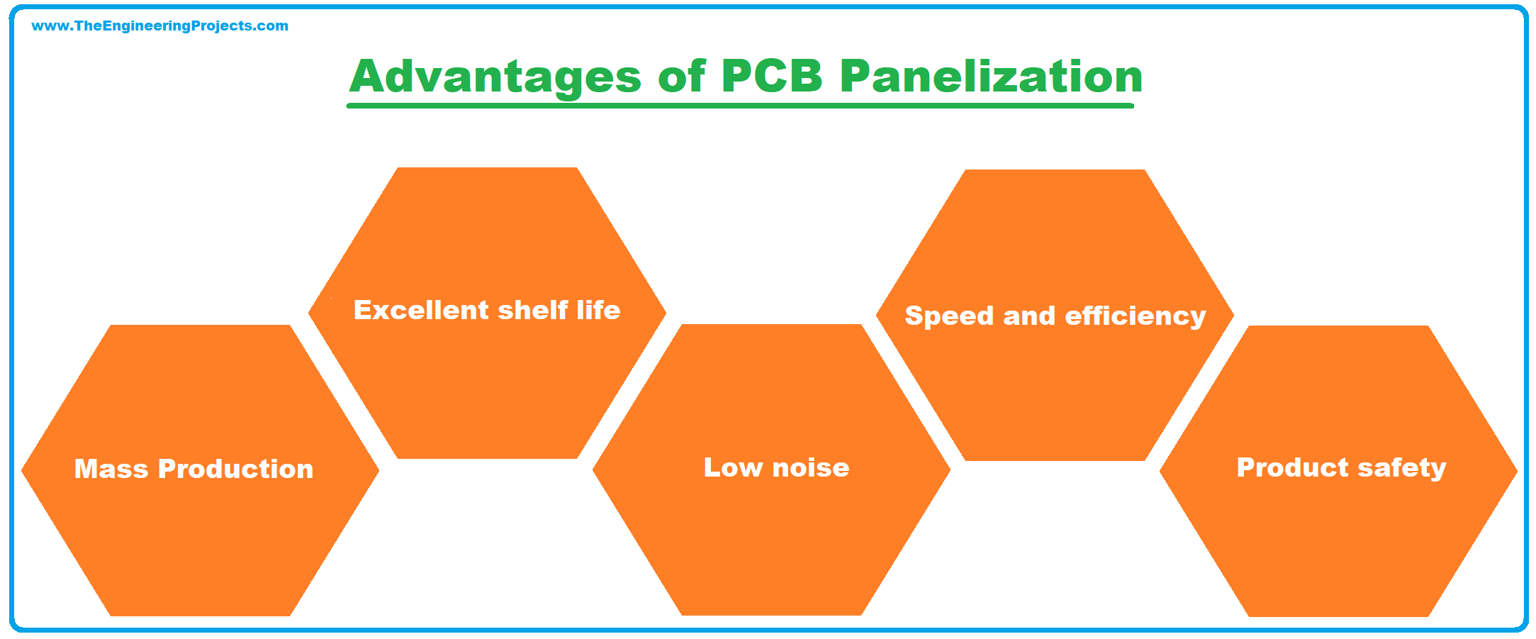
PCB Panelization is not only suitable for producing smaller circuit boards but also leads to an efficient production process. The following are common advantages of PCB Panelization:
- PCB Panelization saves both time and money and is the best technique for the mass production of circuit boards.
- It is a faster and more efficient process to handle multiple smaller boards as part of the large sheet.
- Normally, an 18x24 inch panel size with ½ inch perimeter of board edge clearance is used for the standard panels, however, it is advised to ask for the fabricator’s standard panel size before you even start designing the PCB layout. Since the boards produced using the fabricator’s standard size are cost-effective and help you manufacture multiple boards in less time.
- Product safety is important, especially when you are working in an extreme environment your boards may come across vibrations and shocks as you pass them through the assembly line. PCB Panelization saves your boards from those shocks and ensures the safety of the boards.
That’s all for today. With today's lecture, we have completed the second section of the PCB learning series. In the next section, we will have a look at the Types of PCB boards one by one. Hope you find this article helpful. If you have any questions, you can approach me in the section below. I’d love to help you the best way I can. Thank you for reading this article.


