Hi Guys! Hope you’re well today. Happy to see you around. Today, I’ll walk you through the Introduction to IRF520.
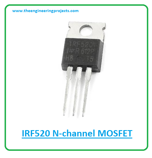
The IRF520 is an N-channel power MOSFET mainly used for switching and amplification purposes. It comes with a breakdown voltage of around 100V and a low gate threshold voltage is 4V, making it an ideal pick for microcontroller applications.
I suggest you read this post all the way through as I’ll detail the complete Introduction to IRF520 covering datasheet, pinout, features, and applications. Let’s get started.
Introduction to IRF520 MOSFET
- The IRF520 is an N-channel power MOSFET mainly used for switching and amplification purposes.
- It comes with three terminals named: gate, source, and drain and is available in the TO-220 package.
- It is important to note that the gate terminal is electrically insulated and contains no current and is normally called an Insulated Gate FET (IG-FET).
- As it’s an N-channel MOSFET so here major charge carriers are electrons as opposed to P-channel MOSFET where major carriers are holes.
- The movement of electrons is better than the movement of holes, making N-channel MOSFET better than P-channel MOSFET.
- Due to better movement of electrons, N-channel MOSFETs with high loads remain cool while P-channel MOSFETs turn hot in the presence of high loads.

- The major charge carriers i.e. electrons enter the channel through the source terminal while they exit the channel through the drain terminal. And the gate terminal controls the biasing of this MOSFET.
- This N-channel MOSFET comes with low on-state resistance of around 0.27 ohm, allowing it to dissipate less energy as heat and consequently increasing the efficiency of the device.
- IRF520 contains a low threshold voltage of around 4V which projects it can be turned on with 5V on the GPIO pins on the microcontroller.
- This chip comes with a decent switching speed, making it an ideal pick for DC-DC converter circuits.
- The continuous drain current (ID) of this device is 9.2A while the drain-to-source breakdown voltage is 100V. The Rise time is 30ns and the fall time is 20nS.
IRF520 Datasheet
Before you apply this component to your electrical project, it’s wise to scan through the datasheet of the component that features the main characteristics of the device. Click the link below to download the datasheet of IRF520.IRF520 Pinout
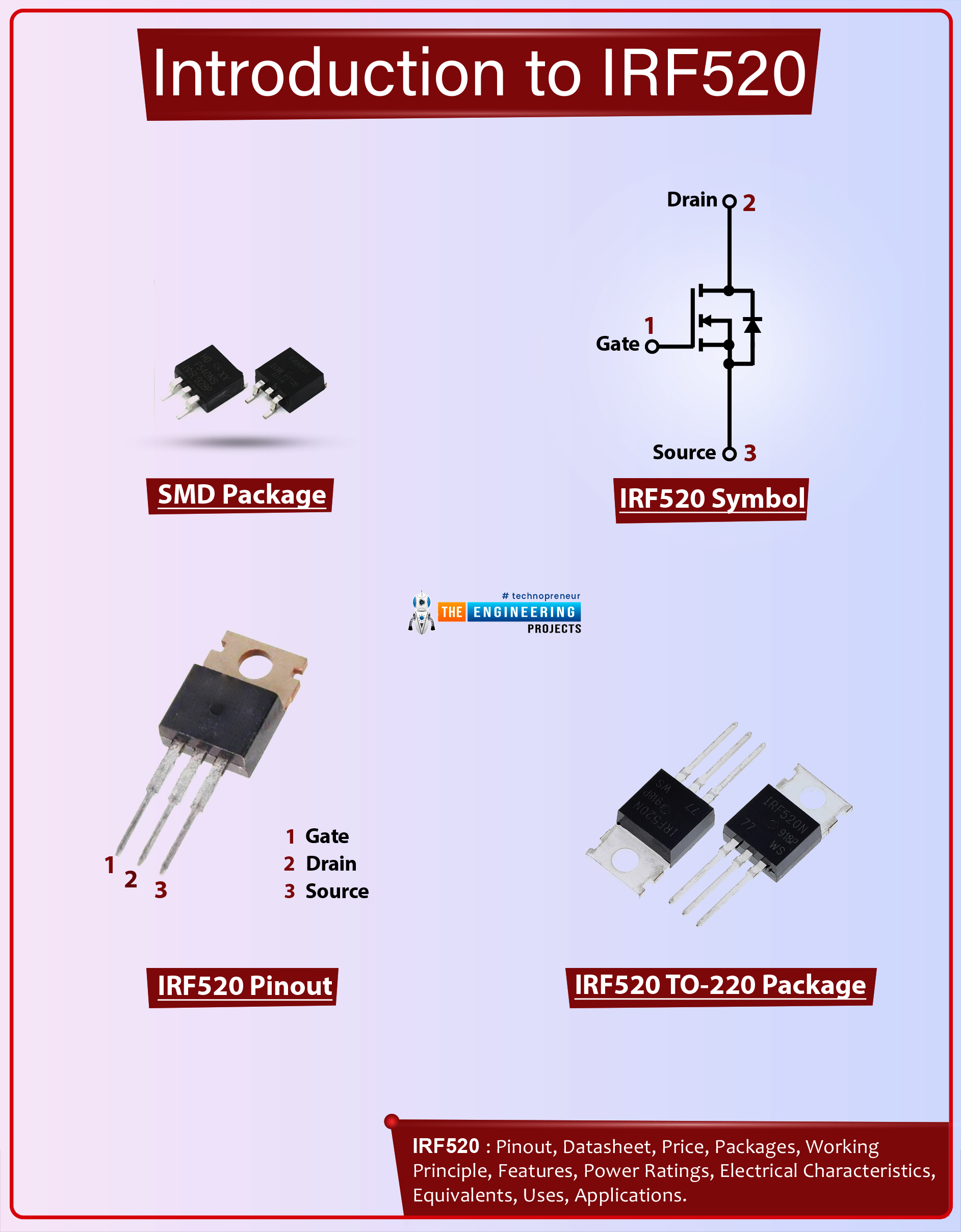
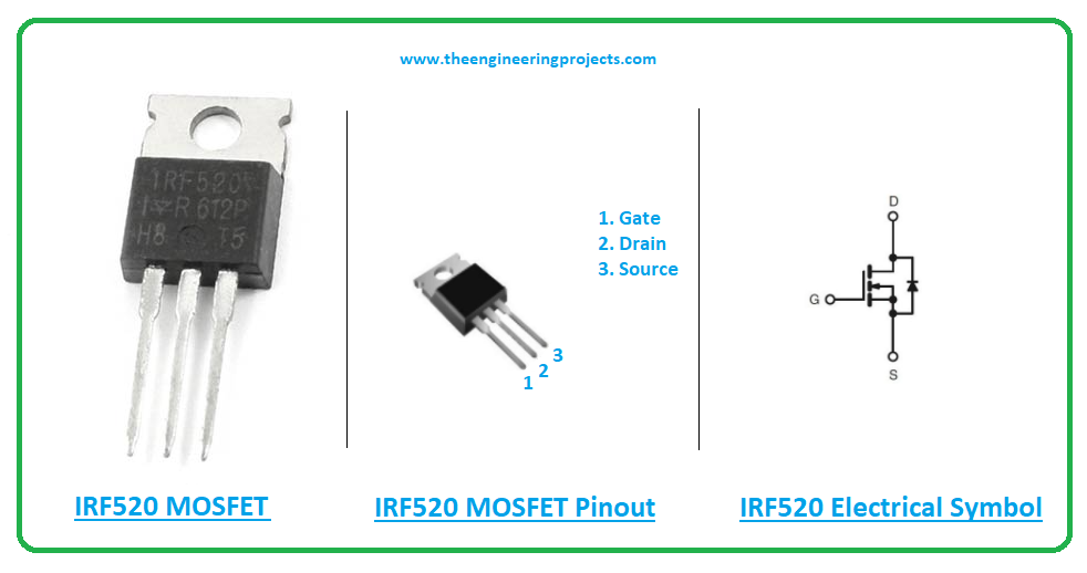
The following figure shows the pinout diagram of IRF520 Mosfet.
| Pin Description of IRF520 | ||||
|---|---|---|---|---|
| Pin No. | Pin Description | Pin Name | ||
| 1 | Used for biasing the device | Gate | ||
| 2 | Electrons leave the channel through a drain terminal | Drain | ||
| 3 | Electrons enter the channel through the source terminal | Source | ||
IRF520 Features
The following are the main features of IRF520 mosfet.- N-Channel Power MOSFET
- Continuous Drain Current (ID) = 9.2A
- Drain to Source Breakdown Voltage = 100V
- Rise time is 30ns and the fall time is 20nS.
- Drain Source Resistance (RDS) = 0.27 Ohms (also known as on-state resistance)
- Since it contains low threshold voltage, it is commonly employed with Arduino applications.
- Gate threshold voltage (VGS-th) = 4V (max)
- Available Package = TO-220 package
IRF520 Applications
The following are the main applications of this device.- Employed to control the speed of motors
- Used in converters or Inverter circuits
- Used in high power devices
- Incorporated in high-speed switching applications
- Used in LED dimmers or flashers
That’s all for today. Hope you’ve got a brief insight into Introduction to IRF520 mosfet. If you’re unsure or have any questions, you can approach me in the section below. I’d love to help you the best way I can. Feel free to share your valuable feedback and suggestions around the content we share so we keep coming back with quality content customized to your exact needs and requirements. Thank you for reading the article.


