
FDV301N N-channel MOSFET Datasheet, Pinout, Features & Applications


Hello Everyone! I welcome you on board. Happy to see you around. In this post today, I’ll walk you through the Introduction to FDB301N.
The FDV301N is an N-channel MOSFET using Fairchild's proprietary and high cell density, DMOS technology. The cell’s high density helps to minimize the on-state resistance. This device is mainly developed for low-voltage applications. This N-channel MOSFET replaces different digital transistors and provides different bias resistor values.
I suggest you read this post all the way through as I’ll detail the complete Introduction to FDV301N covering datasheet, pinout, features and applications. Let’s jump right in.
Introduction to FDV301N
- The FDV301N is an N-channel MOSFET mainly used for switching and low-voltage applications.
- It carries low on-state resistance and can be used in place of different transistors for a range of applications.
- This device contains three terminals named gate, drain, and source. The source is the terminal from which electrons enter the channel and drain is the area where electrons leave the channel. While gate terminal is used for biasing the device.

- The MOSFETs are mainly divided into two main types i.e. N-channel MOSFET and P-channel MOSFET. The N-channel MOSFETs carry electrons as major charge carriers and P-channel MOSFETs contain holes as the major charge carriers.
- The movement of electrons is better than the movement of holes, making N-channel MOSFETs better than P-channel MOSFETs for a range of applications, especially for high-load applications.
- The drain-source voltage of this device is 25V and gate-source voltage is 8V and maximum power dissipation is 0.35W. This is the amount of power it dissipates during the working of this device.
FDV301N Datasheet
It’s wise to go through the datasheet before you apply this component to your electrical project as using this datasheet you can get a hold of the main characteristics of the device. Click the link below to download the datasheet of FDV301N.FDV301N Pinout
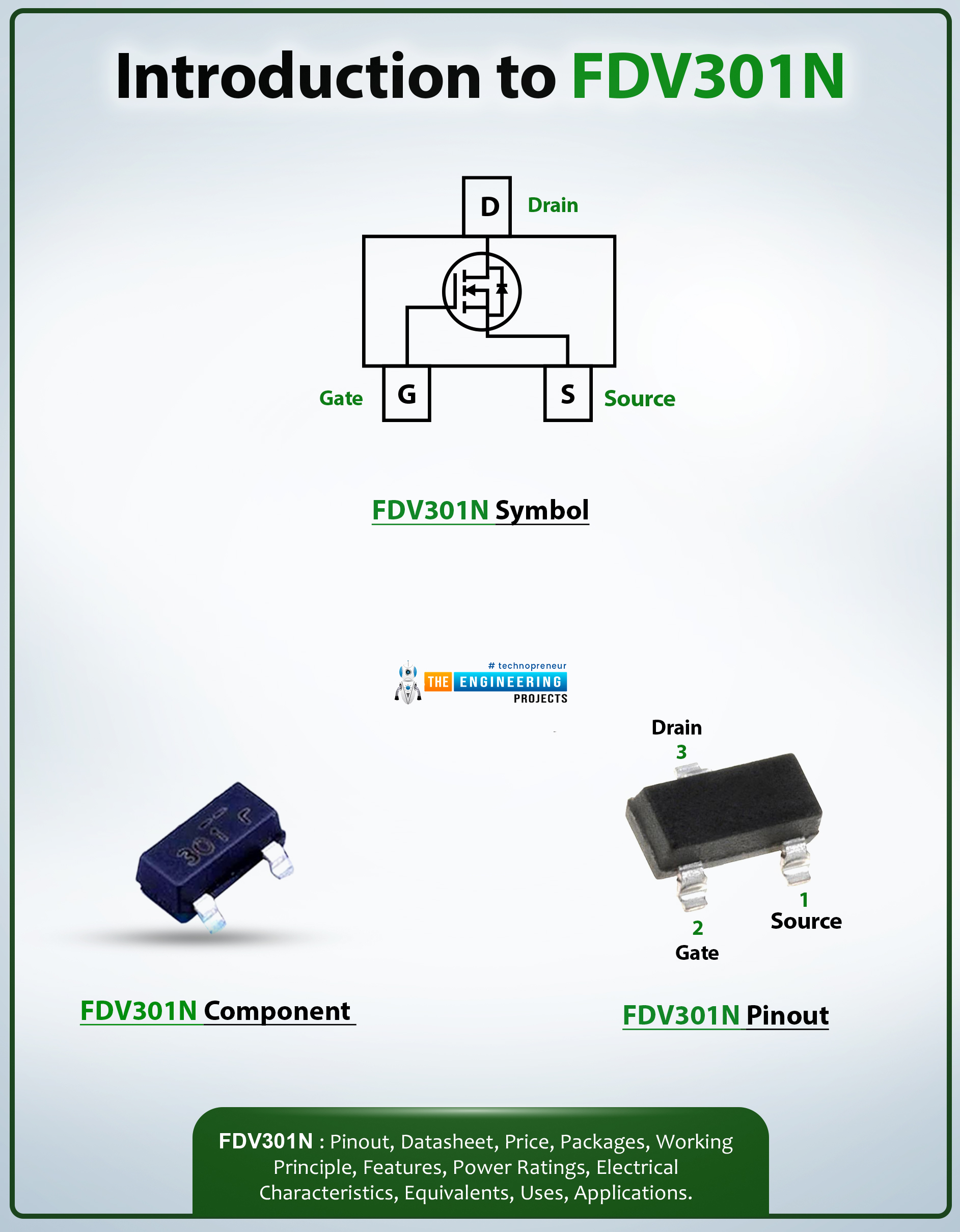
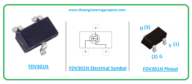
The following figure shows the pinout diagram of FDV301N.
| Pin Description of FDV301N | ||||
|---|---|---|---|---|
| Pin No. | Pin Description | Pin Name | ||
| 1 | Electrons enter the channel through the source terminal | Source (S) | ||
| 2 | Used for biasing the device | Gate (G) | ||
| 3 | Electrons leave the channel through the source terminal | Drain (D) | ||
FDV301N Features
The following are the main features of FDV301N.- The RDS (on-state resistance) is a resistance between drain and source terminal that is 5? at gate-source voltage VGS of 2.7V and it’s 4? at VGS of 4.5V.
- The gate-source voltage (VGS-th) is 8V
- Drain Source Voltage (VDS) is 25V
- Continuous Drain Current (ID) is 220mA
- Level gate drive requirements are very low, helping direct operation in 3V circuits.
- The high-density cell process ensures low on-state resistance RDS (ON).
- This device is reliable and rugged.
- The operating and storage temperature range is -55C to 150C.
- Comes in a compact industry-standard SOT-23 surface-mount package.
FDV301N Applications
This N-channel MOSFET chip is used in the following applications.- Incorporated in low voltage low current applications.
- Employed as switching devices in electronic control units.
- Used in automotive electronics.
- Used as power converters in modern electric vehicles.
- Used in servo motor control.
That’s all for today. Hope you’ve got a brief insight into the Introduction to FDV301N. If you have any query, you can share your comment in the section below, I’ll help you the best way I can. Feel free to share your valuable feedback and suggestions around the content we share so we keep producing quality content customized to your exact needs and requirements. Thank you for reading the article.


 1 user


 Continue Wishlist


 Getting Started Guide
 Help Center
 Contact us
 Doist Blog
 Privacy
 Security
 Terms of Service
 What's new: Channel Descriptions


 Electronic Components
 jameswilson
 0 Comments


 2.3k
2.3k
 953
953
 921
921
 2.1K
2.1K

 Introduction to fdv301n
fdv301n pinout
fdv301n features
fdv301n applications
 Friday, February 5, 2021


