
BSS138 MOSFET Datasheet, Pinout, Features & Applications


Hi Everyone! Hope you’re well today. I welcome you on board. In this post today, I’ll detail the Introduction to BSS138.
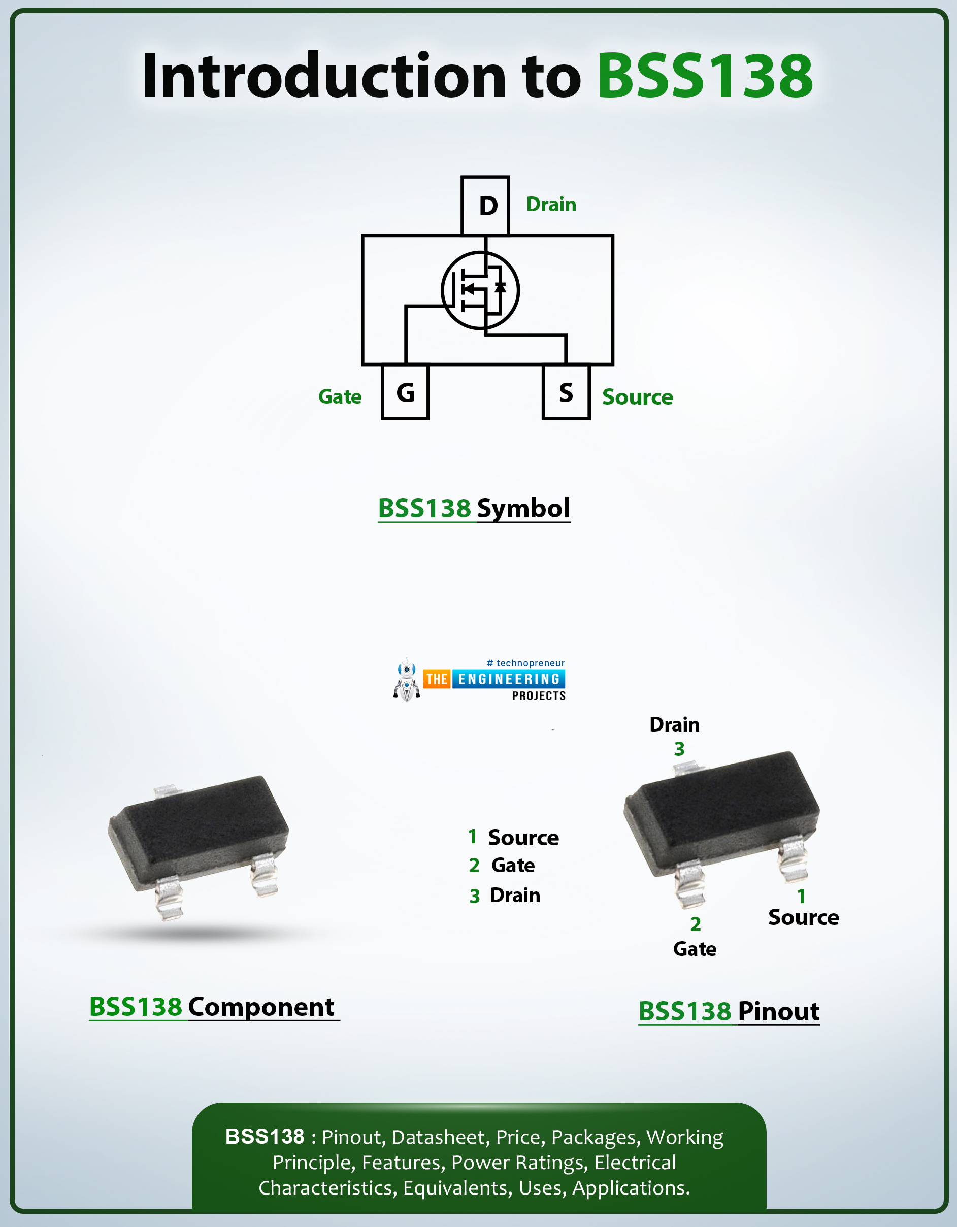
The BSS138 is an N-Channel Logic Level Enhancement Mode Field Effect Transistor that is available in surface mount package SOT-23. It features a low input capacitance of around 40pF and a low on-state resistance of around 3.5. High switching speed and low threshold voltage make this device an ideal pick for level shifter circuit applications.
I suggest you read this post all the way through as I’ll walk you through the complete Introduction to BSS138 covering datasheet, pinout, features, and applications. Let’s jump right in.
Introduction to BSS138
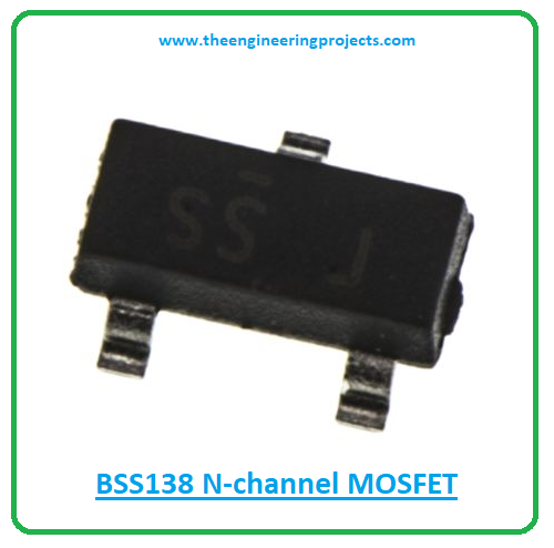
- The BSS138 is an N-Channel MOSFET mainly used in low current and low voltage switching applications.
- It contains three terminals called, drain, source, and gate. At times the body is also included in the terminals, making it a four-terminal device.
- It is important to note that the gate terminal is electrically insulated and contains no current and is normally called an Insulated Gate FET (IG-FET).
- MOSFETs are categorized into two main types i.e. N-channel MOSFET and P-channel MOSFET. This chip BS138 falls under the category of N-channel MOSFET where electrons are major carriers. While holes are major carriers in P-channel MOSFETs.
- The electron movement is better than the hole movement. The reason, N-channel MOSFETs are preferred over P-channel MOSFETs for a range of applications.
- During working with high loads the P-channel MOSFETs turn hot while the N-channel MOSFETs remain cool.
- BSS138 comes in a continuous drain current of around 200mA and drain-source VDS voltage is 50V.
- The on-state resistance of this chip is 3.5, while the turn-off and turn-ON time is 20ns each.
- The compact and robust nature of this device makes it an ideal choice for portable applications including power management circuits and cell phones.
- The BSS138 is costly compared to its alternative 2n7002. Picking the alternative, you have to compromise with the threshold voltage and on-state resistance.
BSS138 Datasheet
Before you incorporate this component into your electrical project, it’s better to scan through the datasheet of the component that highlights the main characteristics of the device. You can download the datasheet of BS138 by clicking the link below.BSS138 Pinout
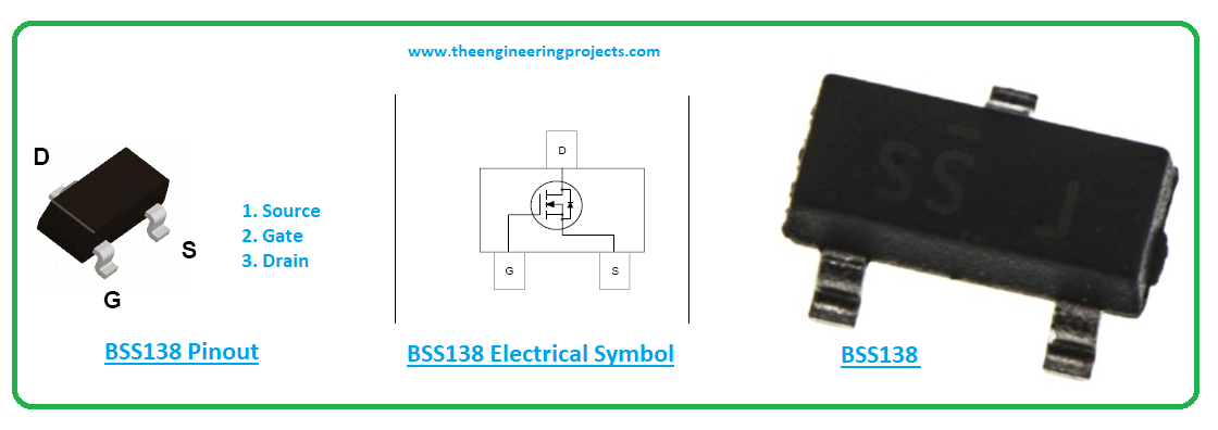
The following figure shows the pinout diagram of BSS138.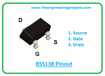
| Pin Description of BSS138 | ||||
|---|---|---|---|---|
| Pin No. | Pin Description | Pin Name | ||
| 1 | Electrons enter the channel through the source terminal | Source (S) | ||
| 2 | Controls the biasing of the component | Gate (G) | ||
| 3 | Electrons leave the channel through the drain terminal | Drain (D) | ||
BSS138 Features
The following are the main features of BSS138.- Logic Level N-Channel MOSFET
- Turn ON and Turn OFF time = 20ns each
- Continuous Drain Current (ID) = 200mA
- Comes in low on-state resistance
- Gate threshold voltage (VGS-th) = 0.5V
- On-state Resistance = 3.5?
- Drain Source Voltage (VDS) = 50V
- Gate threshold voltage (VGS-th) = 1.5V
- Available Package = SOT23 SMD
BSS138 Alternatives
The following are the alternatives to BSS138.- IRF540N
- IRF3205
- IRF1010E
- 2N7000
- BS170N
BSS138 Applications
This chip is used in the following applications. Used in automotive electronics.- Employed as switching devices in electronic control units.
- Incorporated in low voltage low current applications.
- Used in automotive electronics.
- Used as power converters in modern electric vehicles.
- Used in servo motor control.
That’s all for today. Hope you’ve got a brief insight into the Introduction to BSS138. If you have any questions, you can approach me in the section below, I’d love to help you the best way I can. You’re most welcome to share your valuable feedback and suggestions around the content we share so we keep sharing quality content customized to your exact needs and requirements. Thank you for reading the post.


 1 user


 Continue Wishlist


 Getting Started Guide
 Help Center
 Contact us
 Doist Blog
 Privacy
 Security
 Terms of Service
 What's new: Channel Descriptions


 Electronic Components
 jameswilson
 1 Comments


 2.3k
2.3k
 953
953
 921
921
 2.1K
2.1K
 Introduction to bss138
bss138 pinout
bss138 features
bss138 applications
 Thursday, February 4, 2021