D-Type Flip Flop Circuit Diagrams in Proteus

- What are D-Type Flip Flop?
- Which is the IC of D Flip Flop in Proteus ISIS?
- How is the working of D Flip Flop?
- How can we design the Truth Table of D Flip Flop?
- How can we Perform the formation of D Flip Flops in Proteus ISIS?
D-Type Flip Flops
D-Type Flip Flops are important Logical Circuits and we Introduce it as:"The D-Type Flip Flop is a type of Flip Flop that captures the value of D input for a specific time of the Clock edge and show the output according to the value of D at that time."D-Type Flip Flops have the ability to Latch or delay the DATA inputs and therefore are the improved version of the SR Flip Flop (In which the data shows the Invalid output when the inputs are HIGH) . Recall that Flip Flops are the Logical Circuits that can hold and store the data in the form of bits and are important building blocks of many of electronic devices and circuits.
DID YOU KNOW???????????????????????? The D Flip Flop is also known as the Data Flip Flop.When we observe the circuit of D Flip Flop we observe 2 Important points in the D flip Flops:
- The D Flip Flop is the circuit of active High SR Flip Flop that have the S and R inputs connected together with an invertor gate so that both S and R (looking with the point of view of SR Flip Flop) will always have the opposite state to each other.
- The circuit has only one input called D input and it always has a clock that has one of the major effect at the output of D Flip Flop.
D Flip Flop IC
IC's play a magical role in the world of electronics. They make the circuit so simple and decrease the chances of the errors in the circuit. for D Flip Flop, the IC Used has a number CD4013 and for better understanding, D Flip Flop IC named 4013 is shown in the Proteus software in the image below: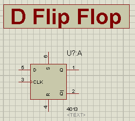
Working of D Flip Flop
In the working of D type Flip Flop, we observe that the D is the only input of the D Flip Flop. yet, the Clock also has the effect in the output of the circuit. Due to the Latched Circuit of Flip Flops, all this discussion would be pointless if we took the concept in the mind that at every pulse, the data of the Flip Flop is changed. Truss, we use an Enabler or Clock in the Circuit through which we can separate the circuit from the input at the instance of our will. When clock is HIGH: Thus, when the D is set HIGH the circuit is said to be in the "Set" State. By the same token, when the D input is LOW the circuit is said to be in the "Reset" position. Unlike SR Flip Flop, the output Q is same as the value of D input and Q' is the vise versa. When Clock is LOW: During the operation when the Clock or Enable input is LOW, any value at the D does not have any effect on the circuit's output. This position is called the "Don't Care" State of D Flip Flop.Truth Table of D Flip Flop
Based upon the Concepts given above, one can easily design the Truth Table of the D Flip Flop. Let's have a look at the Truth Table.| Inputs | Output | ||
| CLK | D | Q | Q’ |
| 0 | X | No Change | |
| 1 | 0 | 0 | 1 |
| 1 | 1 | 1 | 0 |
Performance of D Flip Flop i Proteus ISIS
To perform the experiment in the software, just follow the simple steps given next.Material Required
- NAND Gate
- NOT Gate
- Logic Toggle
- LED-RED
- Ground Terminal
- Connecting wires
- Fire up your Proteus ISIS.
- Pop the "P" button present at the screen and Write the name of 1st four devices and select them one after the other.
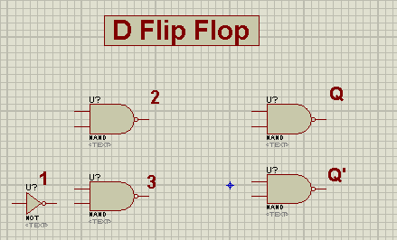
- Arrange four NAND gates and the inverter gate (NOT Gate) at the working area just according to the image given below:
- Take Logic Toggles and arrange them just at the left side of the system.
- Get the LED's for the output and connect one of them with the output of switch Q and Q'.
- Go to Terminal mode>Ground, attach the one ground Terminal with each the LEDs.
- Connect all the devices according to the diagram given next:

- Change the value of the Clock and observe does the value of the output change?
- Turning the LED on means the output is HIGH and vise versa.
- For convenience, the D Flip Flop can also be obtained by using a NAND as NOT in the Circuit as shown in figure:
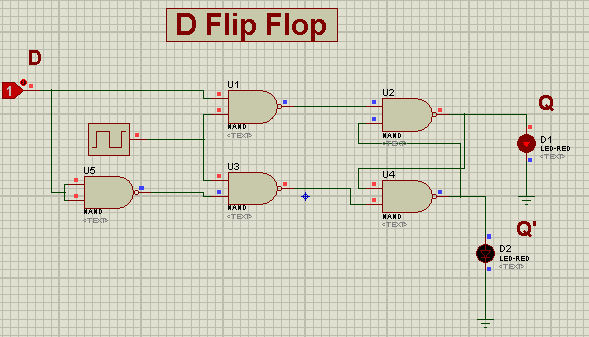
NOTE: You can also use the Logic Probe instead of the Grounded LED. Truss, in this session, we saw what are the D Flip Flops, how does they work, how an we design the Truth Table of D Flip Flop and how can we perform it practically in Proteus ISIS. In the next session, we'll know what are T Flip Flop and how is its Simulation in Proteus ISIS.DID YOU KNOW?????????????
In real life, the Clock is used in the place of Logic Gate (as shown in the image above) because it automatically changes the direction and change the output of the D Flip Flop.
×
![]()


