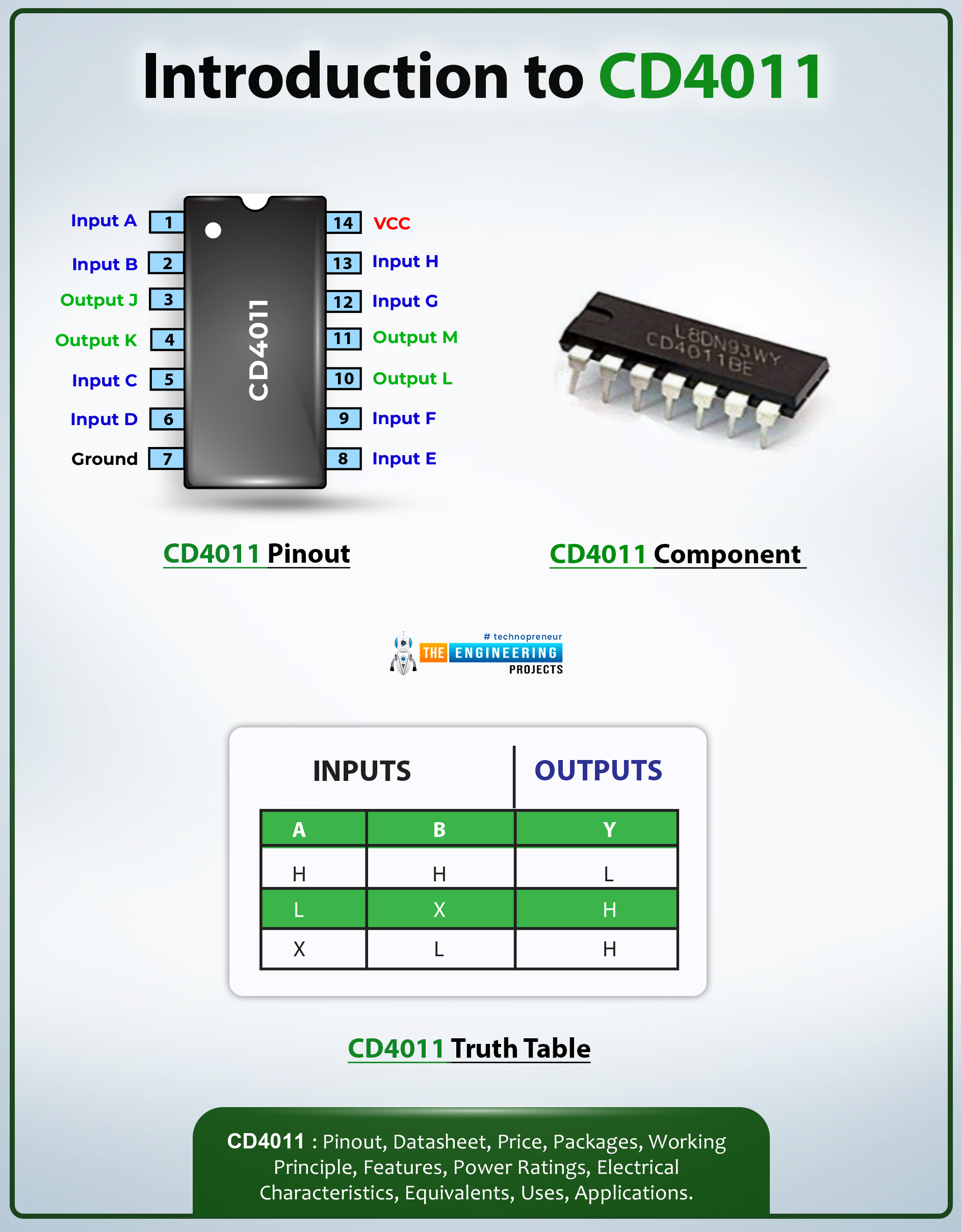
Hi Guys! Hope you’re well today. I welcome you on board. In this post today, I’ll detail the Introduction to CD4035.
CD4011 IC belongs to the CD40xx CMOS IC series. The CD4011 chip comes with four independent NAND gates. This device is used to perform the Boolean function Y = A × B or Y = A + B in positive logic. This IC is widely used in many applications including Portable Audio Docks, AV Receivers, and Blu-Ray Players.
I suggest you read this entire post till the end as I’ll walk you through the complete introduction to CD4011 covering datasheet, pinout, features, truth table, alternatives, and applications. Let’s jump right in.
Introduction to CD4011
- CD4011 IC belongs to the CD40xx CMOS IC series. The CD4011 chip comes with four independent NAND gates.
- It is important to note that the output voltage and the operating voltage of this IC are equal.

- This chip is widely used in many electrical circuits including mp3 players, AV receivers, Blu-ray players, and home theater.
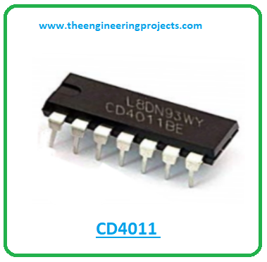
- If you want to use this chip as a logic inverter, you can reconfigure the NAND gates into NOT gates.
- Less transition time makes this device the best pick for high-speed applications.
- The typical operating voltage of this device is 5V which comes in 14-pin PDIP, GDIP and PDSO packages.
- The operating voltage range is -55 to 125C and the propagation delay time is 60ns.

CD4011 Datasheet
Before you incorporate this component into your electrical project, it’s better to scan through the datasheet of the component that comes with the main characteristics of the device. You can download the datasheet of CD4011 by clicking the link below.CD4011 Pinout
The following figure shows the pinout diagram of CD4011.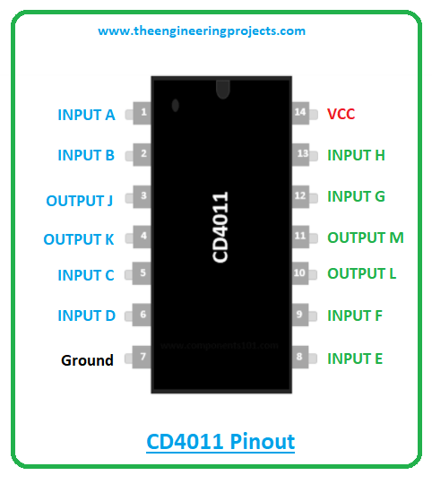
| Pin Description of CD4011 | ||||
|---|---|---|---|---|
| Pin No. | Pin Description | Pin Name | ||
| 1,2,5,6,8,9,12,13 | First Input pin of the NAND gate | NAND Gate Input pins | ||
| 3,4,10,11 | The Inverting input pin of the Op-Amp A | NAND Gate Output pins | ||
| 14 | 5V is used to power the IC | Vcc (Vdd) | ||
| 4 | Connect to the ground | Ground Vss | ||
CD4011 Features
The following are the main features of CD4011.- Typical Operating Voltage = 5V
- Operating Temperature Range = - 55 C to + 125 C
- Low-Level Output Current = 1.5mA
- High-Level Output Current = - 1.5 mA
- Propagation Delay Time = 60 ns
- Dual Input NAND Gate – Quad Package
- Available Packages = 14-pin PDIP, GDIP, PDSO
CD4011 Truth Table
The following figure shows the truth table of CD4011.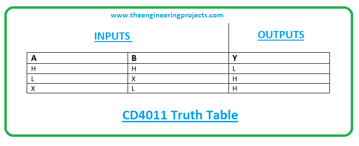
CD4011 Circuit Diagram
The CD4011 circuit diagram is shown in the figure below.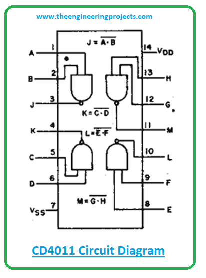
CD4011 Equivalents
The following are the alternative to CD4011.- SN54LS00
- SN74HC00
CD4011 Applications
The CD4011 chip is used in the following applications.- Employed in portable Audio Docks
- Used in AV Receivers
- Used in MP3 Players or Recorders
- Applied in Home Theater
- Incorporated in Blu-Ray Players
- Employed in Personal Digital Assistants (PDAs)
That’s all for today. Hope you’ve got a brief insight into the Introduction to CD4011. If you have any questions, you can pop your comment in the section below. I’d love to help you the best way I can. You’re most welcome to share your feedback around the content we share so we keep sharing quality content tailored to your exact needs and requirements. Thank you for reading the post.


