
74LS76 Dual JK Flip-Flop Datasheet, Pinout, Features & Applications


Hi Folks! Hope you’re well today. Happy to see you around. Today, I’ll walk you through the Introduction to 74LS76.
The 74LS76 comes with separate J, K, clock pulse, direct clear inputs, and direct set. These flip-flops are developed in such a way when the clock is set HIGH, data will be received enabling inputs.
I suggest you buckle up as I’ll detail the complete Introduction to 74LS76 covering datasheet, pinout, features, alternatives, and applications.
Introduction to 74LS76
- The 74LS76 comes with separate J, K, clock pulse, direct clear inputs, and direct set. These flip-flops are developed in such a way when the clock is set HIGH, data will be received enabling inputs.
- This IC contains two JK flip-flops and each flip-flop can be utilized individually for the required applications.

- These flip-flops are mainly employed in control registers, shift registers, and storage registers and are termed as latching devices due to their ability to remember every single bit of data.
- These devices latch the output based on the stored binary data.
- It is important to note more than one flip-flop can be combined in series for storing a small amount of data as an EEPROM.
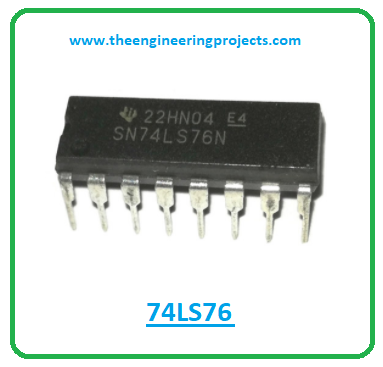
- The operating voltage range of this dual JK flip-flop is 2V to 6V and comes in 14-pin PDIP, GDIP and PDSO packages.
- This JK flip-flop is termed the best pick for practical applications as it possesses stable output for all types of inputs.
- The J and K inputs logic levels will be performed as per the Truth Table as long as minimum set-up times are taken into observation.
- Know that the Input data is converted to the outputs when the HIGH-to-LOW clock transition occurs.
- This IC houses two JK flip-flops and is powered by +5V.
74LS76 Datasheet
Before you apply this component to your electrical project, it’s wise to scan through the datasheet of the component that highlights the main characteristics of the chip. Click the link below to download the datasheet of 74LS7674LS76 Pinout
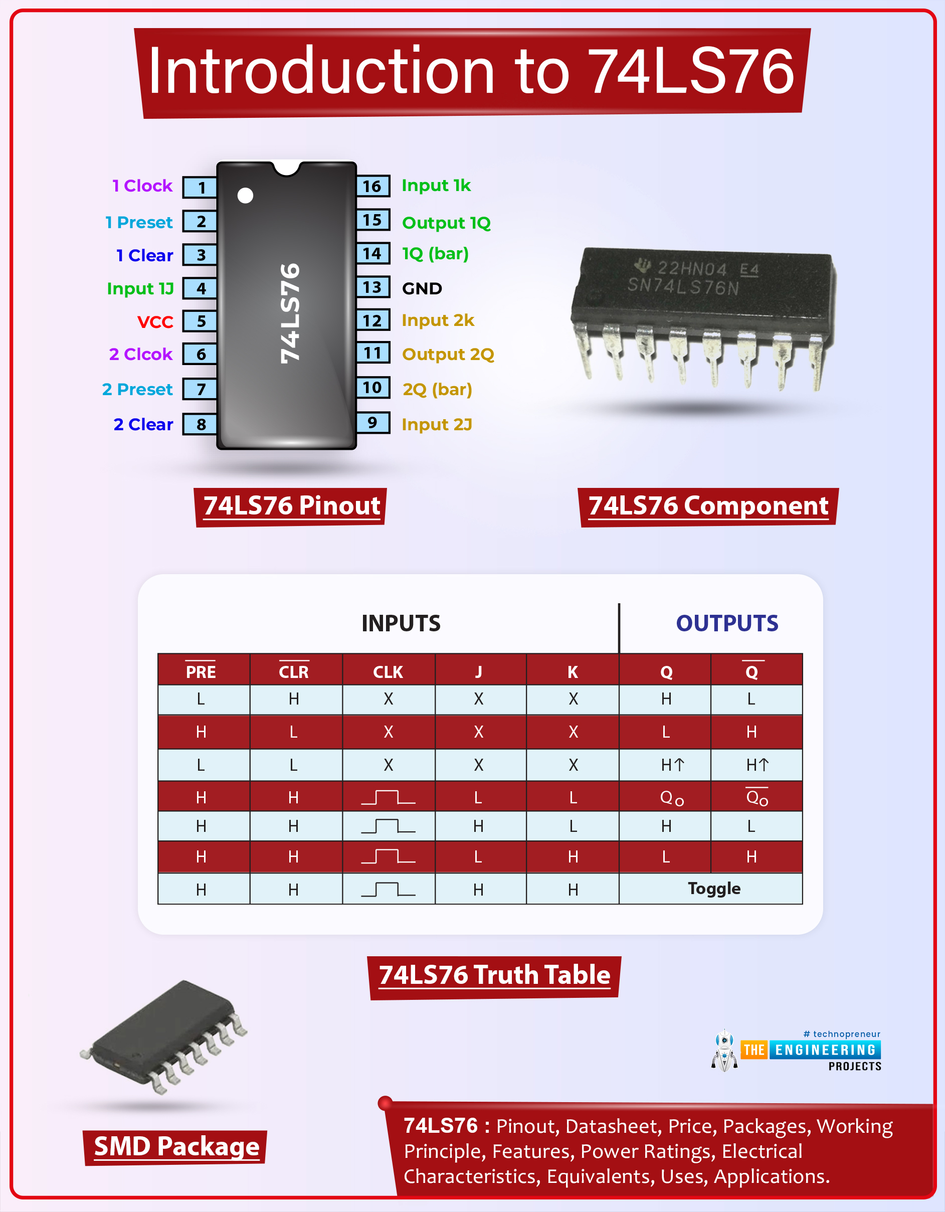
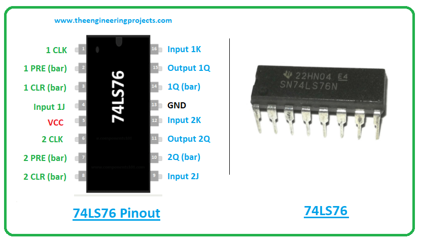
The following is the pinout diagram of 74LS76.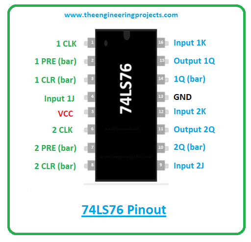
| Pin Description of 74LS76 Dual JK Flip-Flop | ||||
|---|---|---|---|---|
| Pin No. | Pin Description | Pin Name | ||
| 1,6 | These pins should be provided with a clock pulse for the flip flop | Clock-1/ Clock-2 | ||
| 2,7 | Preset input pins drive Flip Flop to a set state. | Preset-1 / Preset-2 | ||
| 16,12 | Input pin of the Flip Flop | 1K/ 2K | ||
| 4,9 | Another Input pin of the Flip Flop | 1J / 2J | ||
| 14,10 | The inverted output pin of Flip Flop | 1Q(bar) / 2Q (bar) | ||
| 15,11 | Output Pin of the Flip Flop | 1Q / 2Q | ||
| 3,8 | Clear input pin drives Flip Flop to a reset state. | 1 CLR (bar)/ 2 CLR (bar) | ||
| 13 | Connected to the ground | Ground | ||
| 5 | Powers the IC with 5V | Power (+Vs) | ||
74LS76 Truth Table
The clear and preset are termed as the asynchronous active-low inputs. When they are set LOW, they result in overriding the J-K and clock inputs allow the output to remain in the steady-state levels. The truth table of 74LS76 is shown below.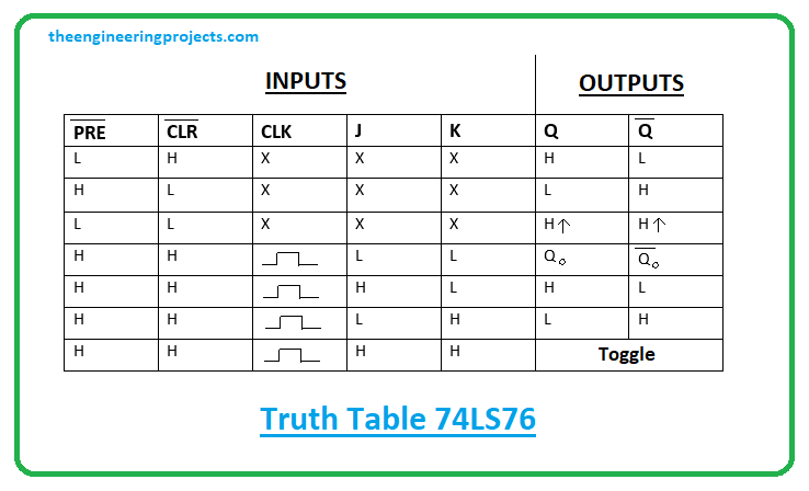
74LS76 Features
The main features of the chip are described below.- Operating Voltage Range = 2V to 6V
- Low-Level Output Voltage Max. = 0.25V
- High-Level Output Voltage Min. = 3.5 V
- Dual JK Flip Flop Chip
- Operating Temperature Range = -55 to -125°C
- Low-Level Input Voltage Max. = 0.8 V
- High-Level Input Voltage Min. = 2 V
- Available Packages = 14-pin PDIP, GDIP, PDSO
74LS76 Applications
The following are the main applications of flip-flop 74LS76.- Employed in Memory/Control Registers
- Used in Shift Registers
- Used in Latching devices
- Incorporated in EEPROM circuits
That’s all for today. Hope you’ve got a clear insight into the Introduction to 74LS76. If you have any questions, you can pop your comment in the section below, I’d love to help you the best way I can. Feel free to share your valuable feedback and suggestions around the content we share so we keep producing quality content tailored to your exact needs and requirements. Thank you for reading the article.


 1 user


 Continue Wishlist


 Getting Started Guide
 Help Center
 Contact us
 Doist Blog
 Privacy
 Security
 Terms of Service
 What's new: Channel Descriptions


 Electronic Components
 jameswilson
 0 Comments


 2.3k
2.3k
 953
953
 921
921
 2.1K
2.1K
 Introduction to 74ls76
74ls76 pinout
74ls76 features
74ls76 applications
 Sunday, January 31, 2021