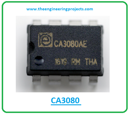
Hi Friends! Hope you’re well today. Happy to see you around. Thank you for clicking this read. In this post today, I’ll walk you through the Introduction to CA3080.
The CA3080 is an operational transconductance amplifier mainly used to convert the input voltage signal into an output current. It is widely used in variable gain amplifiers, frequency oscillators, current-controlled filters, and comparators. It carries an amplifier bias input which is utilized for linear gain control.
I’d recommend reading this entire post all the way through as I’ll detail the complete Introduction to CA3080 covering datasheet, pinout, features, and applications. Let’s jump right in.
Introduction to CA3080
- The CA3080 is an operational transconductance amplifier (OTA) mainly employed in electrical circuits for converting the input voltage signal into an output current.

- In other words, it is an amplifier where the differential input voltage generates an output current. The reason it is termed as a voltage-controlled current source.
- This OTA amplifier is almost similar to the standard amplifier and it carries high impedance and can be employed with negative feedback. It is also applied in the sample and hold circuits.

- The output of this OTA is different from the standard operational amplifier. In OTA the output is current as opposed to the standard amplifier where the output is a voltage.
- Moreover, in linear applications, this OTA is used without negative feedback. And at higher differential input voltages OTA shows non-ideal characteristics due to the input stage non-linearity caused by the input stage transistors.
- The transconductance of this device is directly related to the amplifier bias current means by increasing the bias current its transconductance would increase.
- The CA3080 is available with a remarkable slew rate that makes it an ideal pick for the unity-gain voltage followers and multiplexer.
- When used in multiplexer applications, this device consumes power only during the ON channel state. No power is consumed when the device is present in the OFF channel state.
- This device features a total of 8 pins out of which pin# 8 is not connected while pin# 7 & 4 are voltage supply and ground respectively.

CA3080 Datasheet
Before embedding this device in your electrical project, it’s wise to go through the datasheet of the component that highlights the main characteristics of the device. You can download the datasheet of CA3080 by clicking the link below.
CA3080 Pinout
There are a total of eight pins incorporated into this device. The description of each pin is given below.
| CA3080 Pinout | ||||
|---|---|---|---|---|
| Pin No. | Description | Pin Name | ||
| 1,8 | Not connected | NC | ||
| 2 | Inverting Input | IN - | ||
| 3 | Non-inverting Input | IN + | ||
| 4 | Ground | GND | ||
| 5 | Amplifier bias input | Ibias | ||
| 6 | Output | Output | ||
| 7 | Voltage supply | Vcc | ||
The following figure shows the pinout diagram of CA3080.

Pin# 4 is a ground pin while pin# 7 is a voltage supply pin.
CA3080 Features
- Slew Rate (Unity Gain, Compensated) around = 50V/µs
- Adjustable Power Consumption Range = 10µW to 30µW
- Flexible Supply Voltage Range = ±2V to ±15V
- Fully Adjustable Gain
CA3080 Applications
- Sample and Hold
- Multiplier
- Multiplexer
- Comparator
- Voltage Follower
That’s all for today. Hope you enjoyed this article. If you have any questions, you can pop your query in the comment section below, I’d love to help you the best way I can. Feel free to share your valuable suggestions about the content we share. They help us create quality content customized to your exact needs and requirements. Thank you for reading the article.


